Note: Descriptions are shown in the official language in which they were submitted.
CA 02252348 1998-11-04
97-PDC-399
ELECTRICAL SWITCHING APPARATUS
EMPLOYING BATTERY-POWERED INDICATOR
BACKGROUND OF THE INVENTION
Field of the Invention
This invention is directed to an electrical switching apparatus and, more
particularly, to a circuit interrupter, such as a circuit breaker, including
an indicator
for indication of circuit interrupter status information.
Background Information
Electrical switching apparatus include, for example, circuit switching
devices and circuit interrupters such as circuit breakers, contactors, motor
starters,
motor controllers and other load controllers. Circuit breakers are generally
old and
well known in the art. Examples of circuit breakers are disclosed in U.S.
Patent Nos.
4,751,606; and 5,341,191. Such circuit breakers are used to protect electrical
circuitry
from damage due to an overcurrent condition, such as an overload condition or
a
relatively high level short circuit or fault condition.
Molded case circuit breakers include a pair of separable contacts per
phase which may be operated either manually by way of a handle disposed on the
outside of the case or automatically in response to an overcurrent condition.
Typically,
such circuit breakers include an operating mechanism, which is designed to
rapidly
open and close the separable contacts, and a trip mechanism, which senses
overcurrent
conditions in an automatic mode of operation. Upon sensing an overcurrent
condition,
the trip mechanism trips the operating mechanism to a trip state which moves
the
separable contacts to their open position.
Some trip mechanisms employ a microprocessor to detect various types
of overcurrent trip conditions, such as, for example, a long delay trip, a
short delay
CA 02252348 1998-11-04
- 2 - 97-PDC-399
trip, an instantaneous trip, or a ground fault trip. Some of those trip
mechanisms
employ indicators, such as light emitting diodes (LEDs), to indicate the cause
of the
trip condition by lighting one of the LEDs.
Because circuit breakers are normally powered by current transformers
on the load side of the separable contacts, some trip mechanisms employ
battery-
powered latches and displays to display the cause of the trip. In this manner,
even if
power is removed from the circuit interrupter, the user may determine the
condition
which caused the trip. With the loss of circuit interrupter power, it is not
possible to
recharge the battery or to permanently maintain the charge of the battery.
Hence, there
is room for improvement in battery-powered trip condition indicators for
electrical
switching apparatus.
SUMMARY OF THE INVENTION
This need and others are satisfied by the invention, which is directed to
an electrical switching apparatus. The apparatus includes output means having
means
for outputting one or more status signals provided by a trip means. A battery
means
powers the output means. A modulating means modulates the means for outputting
to
reduce power from the battery means to the output means.
Preferably, the modulating means includes oscillator means for
oscillating with a duty cycle to alternately energize and deenergize the means
for
outputting. The means for outputting may include a plurality of indicator
means for
indicating a plurality of status signals. Each of the status signals, when
active,
cooperates with the oscillator means to energize a corresponding one of the
indicator
means. Otherwise, when each of the status signals is inactive, the oscillator
means is
deenergized to reduce the power from the battery means to the output means.
The electrical switching apparatus comprises separable contact means for
movement between a closed position and an open position. An operating means
moves
the separable contact means between the closed and open positions. The
operating
means has a first state and a second state which corresponds to the open
position. A
trip means senses an electrical condition operatively associated with the
separable
contact means, employs the sensed electrical condition to trip the operating
means to
the second state to move the separable contact means to the open position, and
provides
at least one status signal. An output means cooperates with the trip means and
includes
means for outputting the at least one status signal. A battery means powers
the output
CA 02252348 2006-05-03
-3-
means which further includes modulating means for modulating the means for
outputting to
reduce power from the battery means to the output means.
As a preferred refinement, the output means further includes latch means
powered by the battery means for latching the at least one status signal and
providing at least
one latched signal corresponding to the at least one status signal to the
means for outputting.
The output means may further include means for powering the modulating means
with at least
one of the at least one latched signal to reduce power output by the battery
means to the
output means when each of the at least one latched signal is inactive.
The latch means preferably includes a plurality of latches for latching a
plurality of status signals and outputting a plurality of latched signals to
the means for
outputting. The means for powering the modulating means may include a
plurality of diodes
each of which is connected between one of the latches and the modulating means
to power the
modulating means when at least one of the latched signals is active.
BRIEF DESCRIPTION OF THE DRAWINGS
A full understanding of the invention can be gained from the following
description of the preferred embodiment when read in conjunction with the
accompanying
drawings in which:
Figure 1 is a block diagram of a circuit breaker including a display circuit
in
accordance with the invention;
Figure 2 is a functional block diagram in schematic form of the display
circuit of Figure 1;
Figure 3A is a plot of level at node 104 of Figure 2;
Figure 3B is a plot of the output voltage 114 of the operational amplifier 100
of Figure 2; and
Figure 3C is a plot of the output voltage 162 of the operational amplifier 102
of Figure 2.
DESCRIPTION OF THE PREFERRED EMBODIMENT
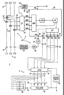
Referring to Figure 1, a circuit breaker 2 including an output circuit, such
as
the exemplary display circuit 4, is illustrated. A typical example of a
circuit breaker is
disclosed in U.S. Patent No. 4,751,606. The circuit breaker 2 includes one or
more separable
contacts 10 electrically interconnected between line terminals 12 and load
terminals 14 for
movement between a closed position (not shown) and an open position (as shown
in Figure 1)
in order to switch one or more electrical currents, such as current 15,
flowing between the
terminals 12,14. The circuit breaker 2 also includes an operating mechanism 16
for moving
the separable contacts 10 between the closed and open positions, and a trip
circuit 18. The trip
,...... . ,._ ,
CA 02252348 2006-05-03
-4-
circuit 18 includes sensors, such as current transformers (CTs) 20, for
sensing the line and
ground electrical currents; a suitable interface (I/F) 22 for receiving the
sensed current signals
24 from the CTs 20; a microcomputer 26, such as a Sure Chip P1usTM; a trip
coil 28 driven by
the microcomputer 26; and a power supply 30, which is self-derived through I/F
22 from CT
current to voltage transformation, providing a voltage +5V to power the
microcomputer 26.
An example of the exemplary Sure Chip P1usTM microcomputer 26 is disclosed in
U.S. Patent
No. 5,270,898. The power supply 30 is powered from the load side of one or
more of the
separable contacts 10.
The microcomputer 26 employs a multiplexer (MUX) to select the sensed
current signals 24 from I/F 22; an analog-to-digital (A/D) converter to
convert the analog
current signals 24 to corresponding digital values; a microprocessor ( P) to
receive the digital
values from the A/D; and a digital input/output circuit (1/0) to input various
input signals (not
shown) and output various output signals, such as signals 32 at output port
lines 34 and signal
35 at output port line 36.
The operating mechanism 16 has a first state (e.g., closed) and a second state
(e.g.; open or tripped) which corresponds to the open position of the
separable contacts 10.
The CTs 20 of the trip circuit 18 sense the electrical current, such as
current 15, flowing
through the separable contacts 10. The P of the microcomputer 26 employs the
digital values
of the sensed current signals 24 from the A/D to generate the trip signal 35
at output 36 for
tripping the operating mechanism 16 through interface (I/F) 37 and trip coil
28 to the tripped
state to move the separable contacts 10 to the open position.
As disclosed in U.S. Patent 4,751,606, the exemplary status signals 32
include status signals representative of a long delay trip, a short delay
trip, an instantaneous
trip, and a ground fault trip of the operating mechanism 16 by the trip
circuit 18. The display
circuit 4 cooperates with the trip circuit 18 and includes lights, such as
light emitting diodes
(LEDs) 38, for displaying the status signals 32.
The display circuit 4 includes the LEDs 38; a battery circuit 40 for supplying
power; an exemplary quad-latch 42 powered by the voltage of the battery
circuit 40 for
latching the status signals 32 and providing corresponding latched status
signals 44 to the
LEDs 38; and a modulating circuit, such as oscillator 46, for
CA 02252348 1998-11-04
- 5 - 97-PDC-399
modulating the LEDs 38 to reduce power from the battery circuit 40 to the rest
of the
display circuit 4. Disposed between the latch 42 and the oscillator 46 is a
diode circuit
48 for powering the oscillator 46. Each of the diodes of the diode circuit 48
is
connected between one of the latches of the exemplary quad-latch 42 and the
oscillator
46 to provide a voltage 50 which powers the oscillator 46 when at least one of
the
latched signals 44 is active. On the other hand, whenever each of the latched
signals
44 is inactive, no power is supplied to the oscillator 46 through the diode
circuit 48,
thereby reducing the power output by the battery circuit 40 to the rest of the
display
circuit 4.
Referring to Figure 2, the display circuit 4 is illustrated. The digital
input/output circuit (I/0) of microcomputer 26 generates four status signals
32 at
outputs 34 (labeled PA4,PA5,PA6,PA7) and one control signal 52 at output port
line
54 (labeled PC5) of Figure 1 for output to the four D-inputs and the CLK-
input,
respectively, of the quad-latch 42. An R-C circuit 55 is disposed at the CLK-
input of
the latch 42 to provide enhanced noise immunity. During a trip operation in
the
microcomputer 26, one of various trip conditions (e. g. , a long delay trip, a
short delay
trip, an instantaneous trip, a ground fault trip) is detected, although a
subset of those
trip conditions and/or a wide variety of other trip conditions are possible.
The
microcomputer 26 designates the trip condition which caused the trip by
asserting one
of the status signals 32 and, then, pulsing the control signal 52 to latch the
status
signals 32 in the D-latches of the exemplary quad-latch 42. In turn, the
latched signals
44 are output by the Q-outputs of the quad-latch 42.
The battery circuit 40 includes a battery 56, such as a Lithium primary
cell, having a voltage 58; an auctioneering circuit 60 for auctioneering the
voltage 58
of the battery 56 and the voltage +5V of the power supply 30 of Figure 1; and
a
reset/test circuit 62 for resetting the latch 42 and testing the battery 56.
The auctioneering circuit 60 includes diodes 64,66 connected at their
cathodes to output a voltage 68 to the VCC power input of the latch 42. The
voltage
58 of the battery 56 is input to the anode of diode 64 through resistor 65 and
the
voltage +5V is input to the anode of diode 66.
The reset/test circuit 62 includes a normally open pushbutton 70,
resistors 72,74, and an LED indicator 76. During a reset/test operation, the
user
depresses the pushbutton 70 which applies the voltage 58 of the battery 56
across the
CA 02252348 1998-11-04
- 6 - 97-PDC-399
series combination of the resistor 65, the closed pushbutton 70, and the
resistor 72
which is in parallel with the series combination of LED 76 and resistor 74. If
the
condition of the battery 56 is good (i. e. , the voltage 58 is of sufficient
magnitude), then
sufficient current flows through LED 76 and resistor 74 to light the LED 76
and, thus,
indicate the good condition of the battery 56. The CLR-input of latch 42 and
resistor
78 form a reset input for clearing the latch 42. At the same time that LED 76
is lit,
the voltage across resistor 72 is applied through resistor 78 to the CLR-input
of latch
42 to reset the latched signals 44 to the inactive state. On the other hand,
if the
condition of the battery 56 is bad, then insufficient voltage is applied
across resistor
72, such that LED 76 is not lit and latch 42 is not reset by the voltage
applied through
resistor 78 to the latch's CLR-input.
Before a trip operation, the display circuit 4 is powered by power supply
30 of Figure 1 through diode 66. During the trip operation, the microcomputer
26 of
Figure 1 outputs a "high" (i. e. , a logic one) on one of its exemplary
outputs,
PA4,PA5,PA6,PA7, to the corresponding D-inputs of the exemplary quad-latch 42.
The logic one is clocked into the appropriate latch of the quad-latch 42 by
the clock
signal 52 on output 54, PC5, also coming from the microcomputer 26. The quad-
latch
42 then sets the corresponding Q-output to a logic one. After the trip
operation, the
power supply 30 is disabled, as the separable contacts 10 are open, and the
power for
LEDs 38 and display circuit 4 is provided from battery 56.
The LEDs 38 include a short delay trip LED (SHORT) 80, an
instantaneous trip LED (INST) 82, a long delay trip LED (LONG) 84, and a
ground
fault trip LED (GND) 86. The anodes of the LEDs 38 are connected to the
corresponding Q-outputs of the quad-latch 42. The LEDs 38 indicate the state
of the
latched signals 44 and, thus, the state of the status signals 32. Although the
exemplary
embodiment indicates, at most, only one of the exemplary status signals 32 at
one time,
other embodiments which indicate two or more of various signals are possible.
The diode circuit 48 includes four diodes 88,90,92,94, the anodes of
which are also connected to the corresponding Q-outputs of the quad-latch 42.
The
cathodes of the diodes 88,90,92,94 are connected in common to form an output
96
which provides the voltage 50 to power the oscillator 46. The diodes
88,90,92,94 are
connected between one of the D-latches of the quad-latch 42 and the oscillator
46 to
suitably power the oscillator 46. Whenever at least one of the latched signals
44 is
CA 02252348 1998-11-04
- 7 - 97-PDC-399
active, the voltage 50 energizes the oscillator 46, with the power input 98 of
the two
operational amplifiers 100,102 being energized through one or more of the
diodes
88,90,92,94. Each of the latched signals 44, when active, cooperates with the
oscillator 46 to energize a corresponding one of the LEDs 38 at a duty cycle
which is
set by the oscillator 46. On the other hand, with each of the latched signals
44 being
inactive, the voltage 50 is essentially at ground potential and the oscillator
46 is
deenergized to reduce the power from the battery 56 to the rest of the display
circuit
4.
Continuing to refer to Figure 2, whenever at least one of the latched
signals 44 is active, the resulting voltage 50 provides a voltage reference
level 103 at
node 104 for the " + " inputs of the operational amplifiers 100,102 as set by
a divider
formed by resistors 106,108. As shown in Figure 3A, the voltage reference 103
has
two voltage level values 110,112 (e. g. ,+0.1 V, +0.75 V, respectively)
depending on
whether the output voltage 114 (as shown in Figure 3B) of the output of
operational
amplifier 100 is high or low. The shift in the voltage reference 103 between
the two
voltage levels 110,112 provides the difference in the resulting "on" and "off'
states of
output voltage 116 (as shown in Figure 3C) of the output of operational
amplifier 102.
On power up of the operational amplifiers 100,102, after the trip
operation, the voltage of the "-" input of operational amplifier 100 is lower
than the
voltage of the " + " input of such operational amplifier and, thus, the output
voltage 114
of the output thereof goes high and charges capacitor 118 through resistor
120. When
the voltage across capacitor 118 reaches about the upper voltage level 112 (e.
g. , about
0.75 V) of the "+" input of operational amplifier 100, the output voltage 114
goes
low, thereby forcing through feedback resistor 121 the voltage 103 at node 104
to the
voltage level 110 (e.g., about 0.1 V). Then, capacitor 118 discharges through
resistor
120 until its voltage reaches about the lower voltage level 110 (e.g., about
0.1 V)
which, in turn, causes the output voltage 116 of the output of operational
amplifier 102
to go high and, also, causes the recharging of capacitor 118.
The LED of interest of the LEDs 38, as selected by the set Q-output of
the quad-latch 42, is lit through resistor 126 when the output signal 116 (as
shown in
Figure 3C) of the output of operational amplifier 102 is a low level 122, and
is
extinguished when that output signal 116 is a high level 124.
CA 02252348 1998-11-04
- 8 - 97-PDC-399
The small amount of energy consumed in the two operational amplifiers
100,102, under a trip condition, provides a large reduction in energy for the
lit LED
of interest of the LEDs 38. The oscillator 46 oscillates to alternately
energize and
deenergize the LED of interest at an exemplary duty cycle of about 12.5 %,
rather than
turning that LED on continuously. Moreover, the period between consecutive low
level pulses 122 may be suitably selected such that the resulting flashing of
the LED
is easily noticed by the user. Although an exemplary 12.5% duty cycle is
illustrated,
the invention is applicable to a wide range of duty cycles which provide
battery power
reduction. For purposes of illustration, but not limitation, an oscillator
having a duty
cycle of about 10% to 20% may be employed.
While specific embodiments of the invention have been described in
detail, it will be appreciated by those skilled in the art that various
modifications and
alternatives to those details could be developed in light of the overall
teachings of the
disclosure. Accordingly, the particular arrangements disclosed are meant to be
illustrative only and not limiting as to the scope of the invention which is
to be given
the full breadth of the appended claims and any and all equivalents thereof.