Note: Descriptions are shown in the official language in which they were submitted.
CA 022~2379 1998-10-20
W O 97/40651 PCT~US97/06370
GRID ARRAY ASSEMBLY AND METHOD OF MAKING
RELATED APPLICATION
This application relates to commonly assigned U.S.
Patent Application Serial No. 08/214,339 filed 03/16/94
in the name of Bruce J. Freyman et al. and the commonly
assigned and concurrently filed U.S. Patent Application
Serial No. 08/637,578 filed 24 April 1996 in the name
of Bruce J. Freyman and Robert F. Darveaux, the
disclosure of which concurrently filed application is
incorporated herein by reference.
BACKGROUND OF THE INVENTION
1. Field of the Invention
This invention relates to packaged grid array
assemblies including integrated circuit chips or dies
and a method of making such assemblies. More
particularly, the invention relates to a method and
resultant article which utilizes standard packaging
equipment and maximizes the yield of manufactured
product at a low cost.
2. Related Art
As integrated circuits have become more complex, a
need has arisen for a packaged integrated circuit
having a large number of high density, reliable
- external package connections. It is also desirable to
include in a packaged integrated circuit one or more
conductive layers for signal routing and provision for
ground and power metallization traces. To meet these
needs, the ball grid array has been developed as
- - illustrated in Fig. 1 of the related application Serial
No. 08/214,339.
A typical ball grid array includes a semiconductor
die, sometimes called herein an integrated circuit (IC)
or chip, attached to a die attach surface on a printed
circuit board (PCB) with adhesive. Electrically
conductive bond pads on the die are connected by
.
CA 022~2379 l998-l0-20
W O 97/40651 PCTrUS97/06370
electrically conductive bond wires to electrically
conductive traces and/or electrically conductive
regions formed on or adjacent to the die attach surface
of the substrate. Electrically conductive vias are
formed through the substrate from the traces and/or
regions on the die attach surface to a mounting surface
of the substrate opposite the die attach surface. The
electrically conductive traces formed on the mounting
surface extend to solder pads formed on the mounting
surface. Solder bumps are formed on each of the solder
pads. The solder bumps are reflowed to attach the
substrate to a larger mother board. An encapsulant
such as plastic is formed to enclose the semiconductor
die, the bond wires and a portion of the die attach
surface of the substrate including most of the traces
and/or regions. The vias are shown outside the
encapsulant but can be inside the encapsulant. The
encapsulant is frequently formed by injection or
transfer molding or by conventional molding equipment
to form the encapsulant over the die in a ball grid
array. Liquid (glob top) encapsulant also can be used.
Recent related art is seen in the illustration of
a wire bond TBGA (Tape Ball Grid Array) l-Metal
Microflex Circuit published by the Electronic Product
Division of 3M where an IC chip is adhered to a
stiffener/heatsink with a polyimide tape first surface
containing metallization, wire bonded to the chip and
providing conductive vias, outside of a central
encapsulant over the chip and bond wires, to solder
balls on an opposite surface of the tape.
Currently, molded plastic BGAs are assembled using
a printed circuit board (PCB) strip containing multiple
BGA (_all ~rid array) circuits that is rectangular in
shape. A single unit BGA image is step and repeated on
the PCB strip in order to maximize productivity during
assembly. In this way, several BGAs are processed at
CA 022~2379 1998-10-20
W O 97/40651 PCTrUS97/06370
the same time in many of the assembly processes. The
PCB strip format also helps to reduce material handling
expense in other areas of the assembly process that
operate on only site at a time.
one of the problems with procuring PCBs in strip
form that have step and repeated BGA images is that the
PCB vendor needs to provide 100% good units on the PCB
strip so that the assembly facility does not process
"bad" units. If the vendor or in-house manufacturing
operation fabricates BGAs in strip form and includes a
bad BGA image, all of the remaining good BGA images on
the strip have to be thrown away. If the BGA assembly
facility accepts bad BGA images on each strip, then the
throughput of certain assembly processes is reduced
because "bad" units are being processed. Also, the
cost of the PCBs increases if the vendor cannot ship
PCB strips that contain bad units.
An obvious method of using only "good" units in
the BGA assembly process is to have the PCB vendor
supply all good PCBs in single unit format instead of
in a strip format. The problem with processing singles
in the BGA assembly process is that almost all of the
off the shelf assembly equipment used by industry today
is configured to run PCBs in the strip format. The
other drawback of processing single unit PCBs is that
the resultant throughput of many of the assembly
processes is reduced as compared to throughput in PCB
strip processing.
In the manufacture of related art devices by
molding operations, it is well recognized that during
encapsulation and subsequent removal of a molding die
section, that the package encapsulant not only encloses
the die and die bonds but also extends along the
surface of the die-mounting substrate where a mold
runner is located leading to a molten encapsulant
supply pot. The excess encapsulant sometimes called
CA 022~2379 1998-10-20
WO97/40651 PCT~S97/06370
"flash" or "bleed", i.e., encapsulant other than that
necessary to enclose the die and die bonds, must then
be removed. However, when the excess encapsulant is
peeled away from the substrate surface, the encapsulant
adheres to the substrate surface, twisting the
substrate and tearing or rupturing the substrate
surface, thereby causing damage to the packaged device.
This damage can be cosmetic (e.g. marring of the
substrate surface) and/or functional (e.g. fracturing
of the substrate; destruction of the electrically
conductive traces on the substrate surface; tearing
away of the solder mask on the substrate surface to
undesirably expose, for instance, copper, and/or
weakening or breaking of the seal between the
encapsulant and the substrate surface).
Further, in production, it is desirable to
integrally form a plurality of substrates in a strip
having alignment holes that are located so as to be
captured by tooling pins of a fixture, allowing the
packaging process (including encapsulation) to be
automated. The excess encapsulant must be removed from
the strip prior to further processing since, if left
attached to the strip, the excess encapsulant extends
past the edge of the strip prohibiting automated
handling in subsequent processes. Adherence of the
excess encapsulant to the substrate during removal of
the excess encapsulant may cause torquing of the strip
that distorts the strip and renders the strip unusable
for further processing. In the first related
application, a novel degating region with noble metal
plating is formed at each runner or gate location such
that the molding compound (encapsulant) bonds weakly
with the plated runner area on the PCB substrate
allowing removal of excess encapsulant without damaging
the remainder of the package assembly.
CA 022~2379 1998-10-20
WO97/40651 PCT~S97/06370
SUMMARY OF THE INVENTION
According to the present invention, the problem of
processing "bad" PCB units on a strip or processing
only good units in a singles format is solved by
receiving only good single units from the PCB vendor or
a manufacturer's own operations and then attaching (or
having the vendor attach) only "good" accepted PCB
units to a disposable or re-usable carrier strip that
is compatible with all of the downstream BGA assembly
processes. The PCB units are preferably formed on a
relatively thin, approximately 0.2 to about l.O mm
thick, epoxy-glass or polyimide glass semi-flexible
substrate or BT-epoxy or other flexible circuit. The
units are attached to the periphery of a series of
spaced apertures in the carrier strip and firmly held
in a position overlying a respective one of the carrier
strip apertures.
An IC die(s) is attached to the PCB and
appropriate wire bonding performed. The invention
specifically allows for standard automolding of the BGA
PCBs in the carrier strip. The carrier strip is
configured so that the molding runner will sit normally
on the top surface of the carrier strip. The BGA mold
cavity of a single molding die, clamps on the top side
of the carrier strip. Mold compound is transferred
over the surface of the carrier strip into the mold
cavity. The mold cavity sits inside the aperture in
the carrier strip. The dimensions of the cavity are
slightly larger (approximately 0.5 mm) than the
resultant molded body dimensions and basically has the
same peripheral shape as the desired molded body. A
hardenably mold compound flows into the opening of the
carrier strip onto each of the single unit PCB attached
to the carrier strip forming the molded encapsulant
body around the die, the die bonds and the
metallization on the PCB's. After the mold compound
CA 022~2379 l998-l0-20
W O 97/40651 PCTAUS97/06370
hardens the molding die opens, and in a separate
operation, the mold runner is removed from the carrier
strip surface and molded package body in a de-gating
operation. The mold runner is not well-adhered to the
carrier strip.
The series of molded packages are transported
through the rest of the packaging process while in the
carrier strip. All-other assembly processes such as
post-mold curing, marking and solder bumping are
accomplished while the molded package is still attached
to the strip carrier. The final ma~or operation in the
BGA assembly process of the invention is singulation of
the single units from the carrier strip. This can be
accomplished in several novel manners. In one
embodiment a v-cut edged, single unit PCB that had been
originally attached to the carrier strip is manually
detached from the carrier strip by exerting a downward
force on the top of the molded package body while
holding the two sides of the PCB which were attached to
the carrier strip. This creates a force on the v-cut
edge of the PCB which results in detachment of the
fully assembled single unit BGA from the carrier strip.
A portion of the PCB which had been attached to the
carrier strip remains behind the carrier strip.
Another method of singulating the individual finished
BGA from the carrier strip is to use a saw. The saw is
used to cut off the excess PCB material which has been
attached to the carrier strip. After sawing through
the PCB the finished BGA package is removed from the
carrier strip. Still another method of removing the
BGA from the carrier strip is to punch through the
carrier strip and PCB at the same time. After punching
the remaining carrier strip can be removed from the
singulated BGA. If desired, the normal metallic (e.g.
copper) carrier strip material can be permanently left
on the BGA PCB to improve the thermal performance of
CA 022~2379 l998-l0-20
W O 97/40651 PCTAUS97/06370
the BGA. In this embodiment, a permanent peripheral
bond between the PCB and the carrier strip is made at
the time the PCB is attached to the carrier strip.
- Other methods such as a tape which loses its adhesion
may be employed.
The method of making a grid array assembly
including a printed circuit board containing multiple
electrical circuits includes the step of providing a
series of printed circuit boards including bonding pads
and metallization on a first surface of each board and
conductive vias in the board extending to a second
opposite second surface of the board, the second
surface containing an array of contact pads in contact
with the vias, which boards have been tested and
determined to be accepted boards. The ensuing steps
include providing an elongated carrier strip having a
series of aligned apertures extending longitudinally
along the strip for mounting individual accepted
boards; attaching an individual accepted board in each
aperture; mounting an integrated circuit die including
die conductive pads, on the first surface; bonding wire
bonds from the die conductive pads to the board bonding
pads; encapsulating the die and the wire bonds against
a portion of the first surface of the boards; and then
after any other finishing operations including forming
interconnection ball bumps, removing a completed grid
array assembly, including the printed circuit board and
die assembly from the carrier strip.
An article of manufacture is disclosed comprising
a series of pre-tested and pre-accepted printed circuit
boards mounted in seriatim in apertures extending
longitudinally along an elongated carrier strip, each
of the circuit boards having an outer peripheral edge
connected to an inner peripheral edge of the carrier
strip bounding the apertures in the carrier strip, the
carrier and the circuit boards being adapted for use in
.
CA 022~2379 l998-l0-20
W O 97/40651 rCTAUS97/06370
assembling the circuit boards into grid array packages
each including an integrated circuit, wire bonds and an
encapsulant.
8RIEF DESCRIPTION OF THE DRAWINGS
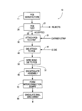
Fig. 1 is a block flow diagram of the method
according to an embodiment of the invention for forming
a grid array assembly.
Fig. 2 is a plan view of a carrier strip showing
on the right side a molded grid array package therein.
Fig. 3 is a plan view of a carrier strip section
showing an obverse side of a mounted printed circuit
board prior to die mounting, wire bonding and
encapsulation.
Fig. 4 is a plan view of a strip section showing a
reverse side of two printed circuit boards prior to
forming ball bonds on an array of contact pads.
Fig. 5 is a schematic side partial view of a
molding die and cavity for encapsulating the grid array
die and wire bonds.
Fig. 6 is a schematic side view partially in
cross-section showing the start of automolding
operation of encapsulating a mounted die and wire
bonds.
Fig. 7 is a schematic side view partially in
cross-section showing the encapsulated die and wire
bonds.
DETAILED DESCRIPTION
According to the invention, a substrate-based
packaged electronic device, such as a ball grid array
including an IC die, is produced by an automolding
process. A series of conforming (the same) generally
planar printed circuit boards (PCB) are manufactured
with suitable conductive traces (metallization), an IC
CA 022~2379 1998-10-20
W O 97/40651 PCT~US97/06370
die attach area(s) and bonding pads on one surface and
an array of contact pads on an opposite surface with
conductive vias extending from the metallization on the
one surface to the contact pads on the opposite
surface. In the past as described above, PCB's have
been manufactured in strip form so that four, six,
eight or more identical PCB's are formed in situ in
strip format. In the present invention, following
manufacturing either singly or on the normal plastic
strip the PCB units are tested to ensure that each PCB
meets a prescribed detailed performance specification.
Any PCB not meeting the specification is rejected.
Those PCB's meeting the specification, herein termed
"accepted" boards, are singulated, if not already in a
single form, and then attached to a disposable or re-
usable carrier strip generally in the form of a strong,
semi-flexible web of copper or stainless or other steel
or other material stock of from about 0.2 mm to about
1.0 mm in thickness. The carrier strip is compatible
with all the subsequent ball grid array (BGA)
manufacture and assembly steps. Each carrier strip has
a series of spaced apertures over which a single PCB is
attached. The invention specifically allows for
standard automolding of each PCB in the carrier strip.
Fig. 1 is a diagram of a process 10 according to
an embodiment of the invention for forming a ball grid
array.
In step 11 the PCB is manufactured with prescribed
metallization including patterned conductive traces of
copper or the like, die attach areas, conductive
bonding pads, conductive vias extending from
metallization on one PCB surface to an opposite surface
forming through board interconnections with an array of
contact pads on that opposite surface.
In step 20 each PCB is tested to the prescribed
performance specification and those PCB not meeting the
_g_
.. ~ . .. ., ~
CA 022~2379 l998-l0-20
W O 97/40651 PCTrUS97/06370
specification become rejects 21. Those PCB's meeting
the specification are accepted boards 22.
In step 30 a prescribed number of the accepted
boards are attached to an incoming carrier strip 31 by
automatic assembly apparatus (not shown) which
attaches, by adhesive bonding, welding, riveting,
soldering or the like, marginal outer peripheral edges
of each PCB to edge margins of a carrier strip
aperture, as described herein with respect to Fig. 2.
A PCB with no marginal outer peripheral edges which is
attachable to the carrier strip by adhesive bonding in
the carrier strip aperture may also be used. In this
embodiment, the area dimension of the accepted boards
is the same as the area dimension, e.g. 27 mm x 27 mm,
as the singulated assembly described below.
In step 40 incoming semiconductor IC dies 41 are
attached to each accepted PCB in a PCB die attach area
using conventional materials such as epoxy or acrylic
or polyimide adhesive, and by conventional processes.
In step 50 the mounted die 41 is wire bonded or
otherwise connected to bonding pads on the PCB to form
an assembly 51.
In step 60, the assembly 51 particularly the die
and wire bonds are encapsulated to enclose the die and
any other electronic device and at least a peripheral
portion of the PCB encircling the die attach area, as
explained in detail below. Briefly a mold die, having
a cavity shaped generally to conform to the to-be-
molded shape of the final BGA package, is positioned
against peripheral edges of the carrier strip aperture
and encapsulant transferred into the mold cavity and
through a mold runner area on the carrier strip until
the cavity is filled.
The encapsulant flows around die 41 and the wire
bonds and adheres to interior portions of the PCB
including metallization surrounding the die attach
--10--
.. .. , . . . . . . ~ .
CA 022~2379 l998-l0-20
W O 97/40651 PCT~US97/06370
area. When the encapsulant hardens the mold die is
removed or opened. Excess encapsulant (bleed) is
formed on the surface of the carrier strip and poorly
adheres thereto. It is easily removed in a later step
by exerting a torqueing or tensile force on the mold
runner attached to the strip carrier. This allows
excess encapsulant to peel cleanly from the carrier and
the package encapsulant without pulling any of the
package encapsulant away from the PCB nor twisting the
PCB so as to damage the resultant packaged electronic
device, either cosmetically, mechanically or
electrically.
In step 70 interconnection bumps, generally in a
solder ball configuration, are formed.
In step 80 each so-formed ball grid array is
singulated from the carrier strip.
Fig. 2 is a plan view of a portion of a carrier
strip 31 showing on the left side an octagonal carrier
strip aperture 32 under which a PCB is to be mounted.
The preferably copper carrier strip includes tooling
holes 33 and 34 which, respectively, are used to align
a PCB 22 against the strip in aperture overlying
position and to position the carrier strip on and with
respect to the various apparati of standard
manufacturing equipment e.g. the mold or wire bonder,
used in the production of a packaged electronic device
such as a BGA, in accord with this invention. As seen
on the right side of ~ig. 2 an accepted PCB 22 having
in one embodiment a 27 mm by 29 mm rectangular size
denoted by dashed outline lines 35 is positioned so as
to underlie aperture 32 with the long ends 35a and 35b
of the PCB 22 extending beyond holes 33. The short
ends overlap the side marginal edges 35c and 35d of the
carrier strip aperture 32 by only about 0.5 mm to about
0.8 mm. The PCB is attached to the carrier strip at
those four overlaps, or at long end overlaps 35a and
--11--
CA 022~2379 1998-10-20
W097/40651 PCT~S97/~370
35b only, by suitable adhesive 56 (Fig. 6). The
adhesive may be a double-sided adhesive tape suitable
for the processing environment to which it will be
subjected, such as Lead Lock tape from Brady Co. of
Milwaukee, Wisconsin or comparable tape from Tomoegawa
of Japan or Pyralux~ adhesive tape from DuPont Co.
After encapsulation to form a molded body 61, a
bevelled encapsulant edge 62 is formed encircling the
body 61 inside a mold shut off area 63. Typical bleed
or mold flash 61b is shown extending on the top surface
of the carrier strip 31. Flash 6la may extend anywhere
on this surface. Upon singulation of the BGA from the
carrier strip in step 80 the finished/completed BGA
package will have a 27 mm. by 27 mm. size with or
without an attached portion of the carrier strip, as
seen by the multi-dashed lines 64.
Fig. 3 illustrates the mounting of a PCB 22
overlying an aperture 32 of a series of apertures in
the carrier strip 31. A die attach area 36 is provided
for mounting the IC die or electronic device.
Metallization traces 37 including gold-plated or other
electrically conductive bonding pads 38 extend over the
top surface of the PCB 22 to vias through one or more
board levels. The standard PCB substrate may be, for
example, epoxy-glass or polyimide-glass or BT/epoxy
(bismaleimide-triazine and epoxy). If multilayer PCB's
are used electrically conductive traces or regions
(e.g. ground planes or power planes) can be formed by
conventional photoresist and masking processes, within
the multilayer substrate and connected to the exterior
opposite surface with conductively plated vias or
through holes formed by well-known techniques including
mechanical or laser drilling and followed by
electroless or electro plating. Annular conductive
rings may be provided at the end of the vias and
connected to the adjacent areas containing the contact
CA 022~2379 l998-l0-20
W O 97/40651 PCTAUS97/06370
or solder pads on which the interconnection bumps will
be formed. The strip 31 further functions as a mold
gate at area 61b and due to the ease of removal of any
flash 61a leaves a clean package outline when the mold
halves 68 and 69 (Fig. 5) are separated.
Fig. 4 shows the reverse or underside of the
attached accepted board 22 where the edges 27 mm. by 29
mm of the PCB are seen by lines 35. Vias 42
interconnect metallization 37 (Fig. 3) and contact pads
39. Interconnect balls or bumps 71 (Fig. 7) are later
formed on contact pads 39. Parallel conductive traces
43 extend from certain bump pads to facilitate
electroplating.
Fig. 5 illustrates the automolding of a package
body 61 by the action of a molding die 68 having a
cavity 64 which clamps against and around the periphery
of the boundary surface edges 65 of the carrier strip
apertures. The inner peripheral edges 66 (Fig. 6) of
the strip aperture act as a stop or dam for the
encapsulant with the strip aperture edges 65 acting as
a mechanical shut-off for the liquid molding compound
e.g. Plaskon molding compound, being dispensed into the
molding die cavity. Arrows 67 indicate clamping of the
mold die against the carrier strip 31 which is backed
by a fixed mold die-supporting surface 69 during the
clamping and encapsulating operations. When
encapsulant is supplied into the cavity (with the top
side of the PCB facing downwardly as shown in Fig. 4) a
mold body 61 with or without a bevelled side edge 62 is
formed upon hardening of the mold compound. A mold
runner 61a (Fig. 3) extends from a mold supply inlet
(not shown) to the mold cavity. For illustration
purposes a non-existent gap is seen between the die 68
and the molded body 61. By molding against the carrier
strip aperture edges poor adhesion of the molding
compound results and the compound does not tenaciously
-13-
. .
CA 022~2379 1998-10-20
WO97/40651 PCT~S97/06370
stick to PCB surfaces, other than at portions within
the mold body surrounding the die attach area.
Fig. 6 shows the portion of the mold die 68
immediately before completion of clamping against the
carrier strip 31. When clamping is completed against
the carrier strip 31, encapsulant is injected into
cavity 64 to encapsulate die 41, wire bonds 55, the
outer edges of the attach adhesive 53 and an annular
portion 58 of the PCB 22. Flash is prevented or
minimized by the clamping force of the molding die
against the carrier strip.
Fig. 7 illustrates the final packaged assembly
resultant from step 70 namely, the forming of
interconnecting bumps, e.g. solder balls 71, on the
contact pads 39 in electrical connection to vias 42 and
to the metallization 37 on and the die 41 mounted to
the PCB. V-cut edge 25 which aids in the singulation
step 80 may be included around the edge periphery of
PCB 22. The substrate is not adhesively bonded to the
carrier strip in the area 56a inside of the V-cut and
is bonded only in area 56b at an interface with the
carrier strip outside of the V-cut, to facilitate the
singulation of each BGA from the carrier strip.
In the singulation step 80 the finished BGA is
broken out by pushing on the package to break it out of
the carrier strip along the V-cut or by punching or
sawing off 1.0 mm of the long sides of the original 27
x 29 mm PCB to result in a 27 x 27 mm packaged device.
An annular ring of copper from around the carrier
strip aperture may be removed or left on to function as
a heat sink and package stiffener to reduce package
warpage. The carrier strip may be reused if no
permanent damage results from excising the assembly
from the carrier strip.
The above description of embodiments of this
invention is intended to be illustrative and not
CA 02252379 1998-10-20
W O 97/40651 PCTrUS97/06370
limiting. Other embodiments of this invention will be
obvious to those skilled in the art in view of the
above disclosure.
. .