Note: Descriptions are shown in the official language in which they were submitted.
CA 02252392 1998-10-16
GR 96 P 1377 - 1 -
Description
Monolithic multilayer piezoelectric actuator and produc-
tion process
Piezoelectric actuators normally comprise a
plurality of piezoelectric elements arranged in a stack.
Each of these elements in turn comprises a piezoceramic
layer which is provided on both sides with metallic
electrodes. If a voltage is applied to these electrodes,
then the piezoceramic layer reacts with a lattice distor-
tion which leads to a usable lengthwise expansion along
a major axis. Since this in turn amounts to less than
two
s parts per thousand of the layer thickness along the major
- axis, a correspondingly higher layer thickness of active
piezoceramic must be provided in order to achieve a
desired absolute lengthwise expansion. With increasing
layer thickness of the piezoceramic layer within one
piezoelectric element, however, the voltage necessary
for
the response of the piezoelectric element also rises.
In
order to keep this within manageable limits, the
thicknesses of individual piezoelectric elements in
multilayer actuators normally lie between 20 and 200 N,m.
A piezoelectric actuator must therefore have an appropri-
ate number of individual elements or layers for a desired
lengthwise expansion.
Known piezoelectric actuators of multilayer
design therefore comprise up to several hundred
individual layers. These can be arranged to form a stack
and, for example, can be adhesively bonded. US 5 438 232
discloses a process for the production of multilayer
actuators by bonding individual actuators with the aid
of
a resin. However, such a bonded stack exhibits too low
a
stiffness for many applications, in particular when high
forces have to be transmitted using the piezoelectric
actuator. Sufficiently high stiffnesses are possessed
by
piezoelectric actuators of monolithic multilayer design.
In order to produce them, piezoceramic green films are
arranged alternately with electrode material to form a
stack and are sintered together. Only in this way is it
- CA 02252392 1998-10-16
GR 96 P 1377 - 2 -
possible to achieve a sufficiently solid composite of the
individual layers in the stack. An article by H. Moilanen
et al. in the journal Sensors and Actuators A , 43 (1994)
357 to 365 discloses a process for the production of a
multilayer piezoelectric actuator in which both the
ceramic layers and the electrode layers are produced by
alternating overprinting. In this case, drying or pre-
sintering at temperatures up to 750°C is necessary at
regular intervals.
An article by S. Takahashi et al. in Ferro-
electrics, 1983, Vol. 90, pages 181 to 190, discloses a
process for the production of a multilayer actuator which
is obtained by stacking ceramic green films printed with
electrode layers on one another and laminating them, and
subsequent sintering of the stack.
In the production of monolithic multilayer
piezoelectric actuators, the material properties both of
the piezoceramic and of the electrode material must be
taken into account during the setting of the process
conditions, in particular during the sintering process.
Problems are posed, for example, by the optimum sintering
temperature for piezoceramic, which, in order to achieve
optimum grain sizes and hence optimum piezoelectric
properties as a function of the composition of the
piezoceramic, may lie above 1250°C. At such a high
l sintering temperature, only platinum can be used as the
electrode material. This exhibits a weak interaction with
the ceramic and can be used together with most piezo
ceramic materials. However, the high material costs for
platinum are disadvantageous, as is the limited strength
at the interface between electrode and piezoceramic.
If Ag/Pd, which is cost-effective and common in
multilayer capacitors, is used as the electrode material,
then the sintering temperature is limited by the melting
point of the alloy, which may, for example, lie below
1130°C (in the case of Ag/Pd 70/30). Hence, one is
limited to piezoceramic materials whose optimum sintering
temperature lies at most at the melting point of the
alloy. To lower the optimum sintering temperature, such
CA 02252392 1998-10-16
GR 96 P 1377 - 3 -
piezoceramics contain B-site dopings of typically 20 to
50 percent in relation to the lead zirconium titanate
(PZT) basic material. As a disadvantage, in the case of
these ceramics a lowered Curie temperature must be
tolerated, which limits the maximum application tempera-
ture of the piezoelectric actuator. In addition, in the
case of this material combination there has also been
shown to be a limited strength in the stack at the
piezoceramic/electrode interface.
It is therefore the object of the present inven-
tion to specify a production process for a piezoelectric
actuator of monolithic multilayer design which is not
limited to piezoceramic material of low Curie and appli-
cation temperature, which nevertheless has good
piezoelectric properties and which additionally possesses
a high mechanical composite strength.
According to the invention, this object is
achieved with a process in accordance with Claim 1.
Special refinements of the invention emerge from further
claims.
With the invention, for the first time a
piezoelectric actuator is produced which has optimum
grain sizes in the piezoceramic layers, irrespective of
any doping which may be present on a B site with an
electrode layer containing silver/palladium. The
piezoelectric actuators possess the optimum values which
are known and expected from a piezoceramic layer of
identical composition which is sintered under optimum
conditions and separately from the electrode layer. In
this case, the piezoelectric actuator has a monolithic
design in which piezoceramic green films and electrode
layers have been sintered together and therefore have a
high strength in the connection between electrode layer
and ceramic layer. The electrode layer, which consists,
for example, of a silver/palladium alloy, remains undam-
aged during the sintering process, since the latter can
be carried out below the melting temperature of the
electrode material. It is particularly surprising that
in
this way it is also possible to obtain a piezoelectric
_ CA 02252392 1998-10-16
GR 96 P 1377 - 4 -
actuator which combines a low or entirely absent B-site
doping, cost-effective silver/palladium electrode layers,
high grain sizes and good piezoelectric properties of the
piezoceramic layers with simultaneous high composite
strength of the individual layers in the stack. In this
way it is possible to obtain, in particular, even
piezoelectric actuators which possess a high Curie
temperature, which enables use of the piezoelectric
actuator at relatively high operating temperatures. This
was previously not known, since piezoceramics with high
Curie temperatures require higher sintering temperatures
than were previously possible with the low melting point
of the electrode layers used. Non-optimum sintering
' conditions at too low a sintering temperature hamper the
grain growth, however, and yield piezoceramics with poor
piezoelectric properties. Good piezoelectric properties,
on the other hand, are obtained if, as in the case of the
piezoelectric actuator according to the invention, the
grain sizes of the piezoceramic layers lie in the same
range from 2 to 10 ~m as is achieved in the case of
sintering the ceramic on its own, that is to say without
electrodes, using a higher optimum sintering temperature.
For the production of the piezoelectric actuator,
likewise acdording to the invention, a starting point is
a known process for the production of monolithic multi
i layer components, in which piezoceramic green films
provided with electrode material are alternately stacked
on one another and are then sintered together. According
to the invention, the starting point is a piezoceramic
powder of the lead zirconate titanate (PZT) type, which
has a stoichiometric composition. In addition to this
stoichiometric composition, a small proportion of a
heterovalent A-site dopant at the level of 1 to 5 mol
percent as well as a further excess of an additional 1 to
5 mol percent lead oxide are added. In addition, an
electrode material containing silver and palladium is
used. The stack is then laminated and sintered under
controlled conditions in an oxidizing atmosphere, the
sintering temperature being allowed to reach at most the
- CA 02252392 1998-10-16
GR 96 P 1377 - 5 -
melting point of the electrode material containing silver
and palladium. The sintering is carried out such that
stoichiometrically excess lead oxide evaporates off and
that, in addition, silver diffuses out of the electrode
layers into the piezoceramic layers, a stoichiometric
piezoceramic composition being obtained.
The invention is based on the surprising knowl-
edge that a hyperstoichiometric' A-site doping, for
example by a higher-valent rare earth metal, can be
compensated during the sintering process by inward
diffusion of silver from the electrode layers. However,
the precondition for this is that at the same time a
stoichiometric excess of lead oxide is present. As an
explanation for this, it is presumed that, during the
sintering process, excess lead oxide produces liquid
phases within the developing piezoceramic structure,
which phases promote the inward diffusion of silver. It
is furthermore surprising that the diffusion process of
the silver is, so to speak, self-regulating. The driving
force for the diffusion process is the heterovalent
defect population of the A sites in the PZT crystal
lattice, which are compensated by the monovalent silver.
When a stoichiometric composition is reached, the driving
force falls away, with the result that further inward
diffusion of silver ceases. Furthermore, it is surprising
about the process that, in spite of a maximum sintering
temperature of, for example, 1130°C for a 70/30
silver/palladium alloy, high grain sizes in the piezo-
ceramic are obtained. It is presumed that the incorpor-
ation of the silver into the piezoceramic promotes the
grain growth. In spite of a sintering temperature which
is reduced by 150 to 200°, just as high grain sizes and
good piezoelectric values are achieved as in the case of
a component sintered under optimum conditions and without
electrodes, and for which correspondingly higher
sintering temperatures can be selected. The achievement
of an optimum density of at least 96 percent is also
shifted to lower temperatures.
As a result of the excess of lead oxide set in
CA 02252392 1998-10-16
GR 96 P 1377 - 6 -
the piezoceram.ic powder, a further advantageous result is
achieved. At the piezoceramic/electrode layer interface,
a phase containing Pd-Pb-O forms as a result of inward
diffusion of palladium, this phase being able to be
detected in the interface region in grain boundary
interstices following sintering. It is presumed that
these phases are responsible for the improved adherence
which has been established between the ceramic layers and
electrode layers in the stack.
In an advantageous way, the sintering is carried
out in an oxidizing atmosphere. Once the maximum
sintering temperature has been reached, a holding phase
of 30 to 120 minutes is maintained at this maximum
temperature.
Both the lead excess and the excess A-site doping
are preferably set to 1 to 3 mol percent independently of
each other. A rare earth, preferably lanthanum or
neodymium, is selected for the A-site doping.
The invention is explained in more detail below
by reference to two exemplary embodiments and the
associated three figures.
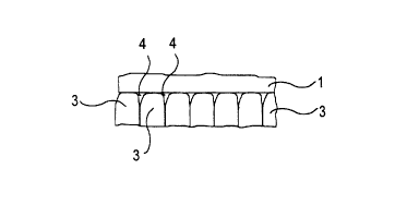
Figure 1 shows a schematic cross-section through an
alternating piezoceramic/electrode stack fol-
lowing sintering.
Figure 2 shows a measured curve for the silver content
of a piezoceramic layer in relation to the
layer thickness following sintering.
Figure 3 shows in the form of a detail a region in the
vicinity of the electrode layer/piezoceramic
layer interface following sintering.
1. Production of a piezoelectric actuator from a
piezoceramic having a high Curie temperature of 330°C.
A piezoceramic powder is prepared which has a
nominal composition of Pbo.98 Ndo,o~ (Zro.ss Tlo.as~ Os.o~~ The
starting materials, mixed as homogeneously as possible,
can be produced in a accordance with known processes and
be constituted, for example, in accordance with the mixed
oxide process or via, chemical routes, for example in
- CA 02252392 1998-10-16
GR 96 P 1377 - 7 -
accordance with the sol-gel process, the citrate process,
the oxalate process or via other organometallic precursor
compounds. Whereas for the mixed oxide process all the
cations provided for the ceramic are mixed with one
another in the fort of their oxides and are then
converted~into PZT, other production processes start from
mixed solutions of organometallic compounds of the
desired cations. By means of precipitation from solution
or by means of gradual thickening in the so-called sol-
gel process, an extremely homogeneous distribution of the
cations in the subsequent solid is achieved.
Following calcining, the product is re-ground,
homogenized and then mixed with an organic binder. Green
films are then drawn or cast using the slip obtained in
this way. Following drying of the green films, these.are
provided with electrode material, for example printed
with a paste which contains particles of a silver/
palladium alloy (70/30 mass ratio) in a binder with an
overall printable consistency.
The piezoceramic green films are produced in a
thickness which, taking into account linear shrinkage
during the sintering of typically 15 percent, yields a
piezoceramic thickness of 20 to 200 N.m. For the electrode
layer, sufficient electrode material is printed on to
yield an electrode layer of about 2 to 3 fcm thickness
after the sintering. Given a small layer thickness ratio
between the electrode layer and piezoceramic layer,
correspondingly more electrode material must be printed
on in order that the process of inward silver diffusion,
leading to an electrode material loss, can be compen-
sated. In this case the electrode layer can be printed
on
over the entire surface or in any desired but as fine as
possible pattern.
The piezoceramic green films, printed with
electrode material, are then stacked on one another, an
alternating arrangement of piezoceramic layer and
electrode layer resulting. By means of a laminating
process under pressure and elevated temperature, the
stack is precompressed and thereafter already exhibits
- CA 02252392 1998-10-16
GR 96 P 1377 - 8 -
sufficient coherence so that it can be handled as a
stack. In this stage, it is also possible to divide a
stack of relatively large base area, following lami-
nation, into a plurality of identical stacks of smaller
base area, for example by means of cutting or stamping.
A plurality of such part-stacks can in turn be combined
to form a larger stack. The total number of the layers
which is required for the subsequent piezoelectric
actuator depends on the level of deflection which is
intended to be achieved using the piezoelectric actuator
by means of applying a voltage. Since an individual
piezoelectric element can be deflected typically by 1 to
2 parts per thousand of its thickness, the required
number of individual layers for a desired total displace-
went can be quite simply calculated via the total layer
thickness of the piezoceramic layers (following
sintering). For example, for a desired application with
a displacement of 20 Vim, about 150 individual piezo-
ceramic layers of about 100 ~.m thickness are sufficient.
Following the lamination of the stack or stacks,
sintering takes place in an oxidizing atmosphere at
1130°C. This maximum temperature is maintained for about
1 hour and is then cooled down slowly.
Figure l: a piezoelectric actuator is obtained
which has a high mechanical composite strength and
therefore a high mechanical loadability. As can be shown
by means of transverse sections through the stack, the
electrode layers 1 are inherently largely coherent. A
high degree of area coverage is thus achieved, which
allows a homogeneous electric field when a voltage is
applied. The piezoceramic layers 2 have high grain sizes
of 2 N,m to 10 ~Cm. An analysis of the piezoceramic yields
the following composition: Pbo.96 Ag o.oz Ndo.os (Zro.s4 Tio.as)
03. The composition is not only stoichiometric but also
homogeneous over the entire piezoceramic layer. This can
be verified, in particular, by a measurement of the
silver concentration by means of microanalysis.
Figure 2 shows the profile of the silver content
as a function of the distance from the piezoceramic
CA 02252392 1998-10-16
GR 96 P 1377 - 9 -
layer/electrode layer interface. It can be seen that the
silver concentration is extremely homogeneous over the
entire layer thickness.
Figure 3 shows, in an enlarged schematic cross
sectional representation, the electrode layer/
piezoceramic layer interface area. The granulation 3 of
the piezoceramic layer can be seen well. The grain
boundary interstices 4 at the interface to the electrode
layer 1, that is to say the interspaces geometrically
predefined by the shape of the ceramic grains, exhibit a
phase in which palladium, lead and oxygen can be
detected. This phase can be detected up to a distance of
50 nm to a few um from the interface to the electrode
layer. It is assumed that, the electrode layer 1 inter-
engages with the piezoceramic layer 2 with the aid of
this phase and contributes to their increased strength
according to the invention. Deeper within the piezo-
ceramic layer or, for example, in the piezoceramic grains
3, no palladium can be detected.
The piezoelectric actuator of this composition is
suitable for application temperatures up to about 150°C.
2. Production of a piezoceramic layer with low
Curie temperature of 170°C.
A piezoceramic powder of the nominal composition
Pbo.99 Lao.oi ~Zro.3o Tlo.3s ~Nli/3 ~i/3~ 0.34~C3.oos is Produced in
accordance with known methods. Corresponding to the first
exemplary embodiment, green films are prepared therefrom,
provided with electrode material, layered to form the
corresponding stacks, laminated and sintered under
identical conditions. A piezoelectric actuator of high
strength is obtained, for which a Curie temperature of
170°C is determined. This actuator can therefore be used
in a temperature range up to a maximum of about 80°C. The
piezoceramic layers 2 have the following stoichiometric
composition after the sintering: Pbo.98 Ago.o~ Lao.o~ ~Zro.3o
T10.36 ~Nll/3 ~2/3~ 0.34~~3
This piezoceramic or, respectively, the
piezoelectric actuator of multilayer design produced from
it, possesses a complex doping for the H site, as can be
CA 02252392 1998-10-16
GR 96 P 1377 - 10 -
seen from the formula. As a result, a piezoceramic with
improved piezoelectric properties is obtained which
exhibits in particular an increased relative deflection.
Added to these improvements in properties, known
per se, as a property'of the invention, is the fact that
an improved strength in the composite of the
piezoelectric actuator is also exhibited here. This
ceramic composition is also stoichiometric following
sintering, since the excess (La) doping is compensated
during sintering by inward diffusion of silver, and
excess lead oxide escapes by evaporating out of the
ceramic. Fiere, too, a uniform silver content over the
ceramic layer results, while palladium can once more only
be detected in areas close to the interface in the form
of the phases containing Pd-Pb-O in the grain boundary
interstices 4 already mentioned in the case of the first
exemplary embodiment.
With the invention it is possible to constitute
a monolithic piezoelectric actuator of multilayer design
which, by comparison with known piezoelectric actuators,
exhibits an improved composite strength, can be produced
with cost-effective electrode layers containing silver/
palladium, and, completely independent of any B-site
doping which may be present, can also be sintered below
an intrinsically optimum sintering temperature to form
a
high-quality ceramic having good piezoelectric
properties. Therefore it is in particular possible to
produce multilayer actuators having application tempera-
tures up to 150C, high mechanical loadability and high
reliability, even in dynamic operation.