Note: Descriptions are shown in the official language in which they were submitted.
CA 022~2611 1998-10-20
GR 96 P 1384
FILF r'~ ~ 9
5 ~ L A~ J
Description
Plug connector with contact area protection in the plug-
in-opening region
The invention relates to a plug connector having
an insulation body which has an essentially rectangular
cross-section and on whose upper side there are arranged
a plurality of electric contact tracks which lie
alongside one another in one plane, run in the plug-in
direction and, when the plug connector is joined to a
mating connector, cooperate with the correspon~;ng
contact springs of the latter, these springs lying
alongside one another, and produce an electric contact.
Plug connectors of this type have become known,
and are of interest, in particular in conjunction with
the stAn~Ardized USB (Universal Serial Bus) design which
i~ the aim of several computer manufacturers. Rather
than, as has hitherto been the case, peripheral devices
being connected to a PC via individual, parallel connec-
tions using separate, and often different, plug connector
systems, this new bus system makes it possible for the
peripheral devices to be connected, essentially in
series, to a common bus line, which is connected directly
to a printed circuit board (motherboard) of the PC via a
stAn~Ardized socket on the housing of the PC. The plug-in
appearance of the printed circuit board socket
treceptacle) is essentially already defined by a
specification and has four strip-like contact springs
which lie alongside one another in one plane and, when
the bus connector (plug) is plugged in, cooperate with
the four contact rails or tracks lying alongside are
another in said plug and produce the electric contact.
The contact springs are arranged in the socket connector
in an insulation body which is essentially designed as a
plastic tongue with a rectangular cross-section, and are
bent over in their rear region to form connecting legs
which project away downwards and can be plugged into
contact holes in the printed circuit board. Connector and
CA 022~2611 1998-10-20
GR 96 P 1384 - 2 -
mating connector are normally provided with a metallic
screening housing. Provided in the top and bottom region
of this shroud are in each case two latching hooks which
engage in recesses on the ~creening housing of the
matching mating connector and produce the earthing
contact and the ret~in;ng forces when the plug is pulled
out.
It is generally the case with plug connectors
that the contact elements of the two components to be
plugged together move towards one another in the plug-in
direction during the plugging-in- operation and move away
from one another in the plug-in direction during the
drawing-apart operation. Outside the end position, the
contact elements may move either with or without contact
with one another. In this arrangement, it is
f~~n~m~ntally desirable to prevent the contact areas from
being exposed to possible damage or cont:~m; n:~ tion. In the
case of the plug connector known from the specification,
recesses for the contact tracks, in which the latter are
retained, are provided in the insulation body, which
forms a closed front on the plug-in side, said recesses
being open towards the upper side. In the case of this
conventional plug connector design, it is unavoidable
that the contact springs of the socket connector are
initially moved over the front region of the insulation
body of the plug when being plugged in. This presents the
risk of non-conducting plastic material coming into
contact with the contact areas and accelerating the wear
(gold abrasion) of the high-~uality-plated contact areas.
This can increase the contact re6istance at the inter-
faces of the plug connector system to such an extent that
the signal transmission is impaired. Sharp-edged contact
of the contact elements can also lead to undesirable gold
abrasion.
The present invention i~ based on the object of
solving the contact-m~k; ng problems outlined.
In the case of a plug connector of the type
mentioned at the beg;nning~ this object is achieved in
that the plug-in end of the contact tracks is in each
.. , . . ~ . . ... ~ ..
CA 022~2611 1998-10-20
- GR 96 P 1384 - 3 -
contact spring, in that the insulation body i8 designed
at it~ plug-in end with a step-shaped offset, the
transition between the levels, at least in each case in
the region of the contact tracks, being designed to match
the curved sliding face of the latter, that is to say as
a rounded step, and in that the contact tracks are
fixedly arranged in the insulation body by being encased
in plastic.
The invention is explained in more detail below
using an exemplary ~mbodiment in conjunction with
figures, in which:
Figure 1 shows a perspective partial view of a plug
connector according to the invention,
Figure 2 shows a partly sectioned view of the plug
connector according to Figure 1,
Figure 3 shows a schematic section of the plug connector
and of a corresponAing mating connector in the
unplugged state.
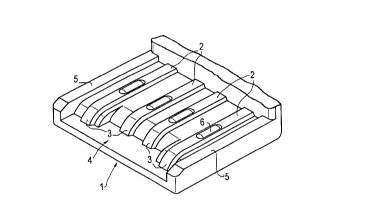
Illustrated in Figure 1 is an insulation body 1
which has at its plug-in end a step-shaped offset 4, 80
that the contact tracks 2, which are arranged at the
higher level, end before the plug-in end of the
insulation body 1. The latter therefore forms at the
plug-in end a front which is not closed but rather is
designed to be open in the plug-in-opening region. The
contact tracks 2 are in each case designed with a curved
sliding face 3. As a result of this and of the open front
region of the insulation body 1, protection is offered
against sharp-edged and/or abrasion-related contact with
the mating connector during the plugging-in operation,
since, according to the invention, the normally likewise
rounded contact point 7 of the contact spring of the
socket connector now cooperates with the sliding face 3
and also no longer has to be moved over a sharp front
edge of the insulation body 1. The offset 4 and the free
face formed thereby accordingly have the effect that the
incoming contact spring, which ~ags downwards somewhat,
does not come into contact with the insulation body 1
prior to ~-lr; ng contact with the sliding face 3.
CA 022~26ll l998-l0-20
GR 96 P 1384 - 4 -
In order to reduce the contact abrasion further,
it i8 advantageous also to provide an offset of the
plastic material at the sides of the contact tracks 2 in
each case, as illustrated in Figure 1. The insulation
body 1 is thus, in principle, to be designed such that it
is set back in all the areas which could interfere during
plugging in.
As can be seen in Figure 1, the insulation body
1 is designed with side edges 5 whose height is dimen-
sioned such that the plastic tongue 8 (cf. Figure 3) ofthe mating connector slides over these side edges 5
exactly at the envisaged height when being plugged in,
with the result that the contact elements 3, 7 of the
socket and plug come into contact with one another as
snvisaged. The further setting back of the two central
contact tracks in relation to the outer contact tracks is
based on the fact that the outer contact tracks are
normally used as power connections and are intended to
form a contact at a point in time before the inner signal
contacts. In the end position, the rounded-off contact
points 7 are in contact with offset contact regions 6,
which are arranged approximately in the centre of the
contact tracks 2.
As a result of encasing the contact tracks in
plastic, these are held precisely in position and cannot
lift off from the insulation body 1, which is of
importance in particular with regard to the curved
sliding face 3. As can be seen in Figure 1, the tip of
the sliding face 3 is anchored in the insulation body 1
in each case in the region of the offset 4. Encasing also
offers the advantage that an additional mounting
procedure (insertion of the contact tracks) is not
necessary.
In Figure 2, for better underst~n~;ng, the two
right-hand contact tracks 2 are illustrated in an
(imaginary) non-encased state. In Figures 1 and 2, for
simplicity, only the plug-in region of the plug connector
is illustrated. The plastic tongue 8 and the contact
point 7 of the contact spring, which sags downwards
CA 022526ll l998-l0-20
GR 96 P 1384 - 5 -
somewhat, of the mating connector can be seen in Figure
3. The plug connector according to the invention is
illustrated here with a shroud 9. In the plugged-in
state, the plastic tongue 8 lies above the insulation
body 1.