Note: Descriptions are shown in the official language in which they were submitted.
CA 02252775 1998-10-23
WO 98/37645 PCT/US98/03668
Method and System for Egualizing PM~
Using Incremental Delay Switching
Background of the Invention
Fie~d of the Invention
The present invention generally relates to fiber optic transmission
and communication of inforrnation, and more specificall~ to a
solution to the problem of Polari7.ation Mode Dispersion.
Related Art
Polar~zation-Mode D~spcrsion rPMD)
Fiber optics technology is revoiu~ionizing the telecommunica~ions
5 field. The main driving force is the promise of extremely high
communications bandwidth. At high bandwidths, a single beam of
modulated laser light can carry vast amounts of information -
equal to hundreds of thousands of phone calls or hundreds of
video channels.
However, pulse broadening limits the effective bandwidth and
propagation distance of an optical communication signal. Because
of the inherent dispersive nature of an optical fiber medium, all
portions of a light pulse do not travel at the same speed through
an optical fiber causing pulse broadening.
Figure 1 illustrates how pulse broadening arises from vaIying light
..... . . .
CA 02252775 1998-10-23
WO 98/37645 PCT/US98/03668
propagation delays which eventually distorts light output. Digital
input pulses lOO are input to an optical flber medium 110. The
amplitude-modulated pulses are generated by a modulated laser
source, such as a direct-modulated laser or an externally-
5 modulated laser.
Different portions of a light puise encounter varying propagationdelays arising from, inter alia, the v~rying leneth~ r f reneetecl paths
within optical fiber llO. For clarity, three paths are illustrated
o which correspond to a relatively straight, short path lOOa, a
reflected, intermediate length path 100b, and a relatively long,
reflected path lOOc. Due to the varying propagation delays, see,
e.g., the ~t delay in arrival time between lOOa and 100b, the
combined optical output is distorted. Thus, a photoreceptor
detecting the output pulses 100a-lOOc will generate a distorted
output 120.
As shown in Figure 2, such pulse broadening can lead to symbol
confusion. "Pulse broadening~ is called "dispersion" or"spreading~
~o because of the non-uniforrn way in which parts of the incident
signal 200 propagate ~hrough a dispersive fiber medium. ~n a mild
form of dispersion, the transitions bet~veen ON and OFF states
obse~ved at a receiver are not as abrupt and distinct as the
transitions that were originated by a transmitting laser. More
~5 severe blurring in the time domain limits the useful bandwidth of
the path.
CA 022.,277F, 1998 - lo - 23
WO 98/37645 PCT/US98/03668
- 3 --
In Figure 2, dispersion effects have broadened two closelv sp~ced
pulses to the extent that they are almost indistinguishable, as
~ndicated by a question mark in the output signal 220. This will
cause an information bit to be received erroneously, with perhaps
disastrous results on network communication and customer
dissatisfaction .
Several refinements have been made to reduce dispersion and
o increase the useful bandwidth. First, single-mode fiber was
developed having a ;lender core such that there is essentially only
a single light path through the fiber. Secondly, the distributed
feedback (DFB) laser ~vas developed with an extremely narrow
distribution of output wavelengths. This technique minimizes
chromatic dispersion caused by the fact that different wavelengths
travel at slightly different speeds through a fi1ber. Finally, a
dispersion-shifted fiber material was produced to minimize the
speed-v.-wavelength dependency at a specific wavelength of fifteen
hundred and fifty nm. common in telecommunication applications.
Cumulatively, recent improvements in fiber materials and
transmitter devices have reduced pulse dispersion and increased
working bandv.~idth. "Lightwave" technology has advanced at such
a pace that the bandwidth capabilities have more than doubled
~5 every two years. As a result, working bandwidths, expressed in
terrns of digital bit-per-second rates, have escalated from 500
.... _ . . . , . . . . ~ -- . . .
CA 02252775 1998-10-23
WO 98/37645 PCT/US98/03668
- 4 -
Mbps to 10 Gbps.
Problem Solvec~ by the ~nvention
These progressively more exotic refinements have brought the
s technolo~y to a new bandwidth barrier: Polarization-Mode
Dispersion (PMD). I'reviously, PMD was insignificant in magnitude
relative to other dispersive effects, but now it is a limiting factor. It
is well known that light can be polanzed and that, ~or a given beam
of light, this polariza~ion can be expressed in terms of two
o orthogonal axes that are normal to the a~is of propaga~ion. As a
beam of light propagates through a fiber, the light ener~y present
along one such polarization may leak into the other polariza~ion.
This leakage would 11OL~11a11Y be of little consequence (lightwave
15 receivers will detect both polari~ations), except that real world
fibers carry different polarizations at slightly different speeds. This
effect can be on the order of 10-20 picoseconds (ps) in a 100 km
fiber and becomes important when the modulating pulses are 50-
100 ps. in width. To complicate matters, the polarization
20 dispersion within a given fiber changes as a function of time and
temperature. Therefore, an effective PMD compensation
mech~ni.~m must monitor and adapt to the changes so as to keep
PMD to a rninimum.
25 To nullify the effects of PMD, researchers have suggested
application of an adaptive compensation device in an optical path
CA 02252775 1998-10-23
WO 98/37645 PCT/US98tO3668
- 5 -
at the receive end just before the receiving transducer. These
compensators typically employ a detector for anaiyzing the relative
partitioning and dekly of the incoming signal along two orthogonal
polarizations. The compensators correct a data signal by
s purposefully adding delay selectively to one polarization or
another. A controller interpre~s the findings of the delay analyzer
and manipulates adjustable delay elements so as to compensate
for the polarization-c~ependent delay differences caused ~ the
imperfect fiber transmission path. However, Lhes~ techniques are
not practical in telecommunication applications, such as, long-
haul optical fiber cornmunication.
The variable delay el~ments are usually optical fibers that are
either heated or squeezed to alter their propagation characteristics.
While these elements are adaptable to laborator~ electronic control
techniques, they are inadequate in terms of reproducibility and
predictability of response. They are also impractical for use in a
commercial traffic-bearing fiber networlc wherein recovery time
following an equipment or power failure should be minimi~ed. See,
20 e.g., Ozeki, et al., "Polarization-mode-dispersion equalization
experiment using a variable ec~llAli~ing optical circuit controlled by
a pulse-waveforrn-comparison algorithm,~ OFC '94 Technical Digest,
paper TuN4, pp. 62-64; Ono, et al., "Polarization Control Method
for Suppressing Polarization Mode Dispersion Influence in Optical
Transmission Systems", Joumal of ~ightwave Technology, Vol. 12,
No. 5, May 1994, pp. 89-91; T~k~h?si, et al., "Automatic
. .
CA 02252775 1998-10-23
WO 98/37645 PCT/US98/03668
- 6 -
Compensation Technique for Timewise Fluctuating Polarization
Mode Dispersion in In-line Amplifier Systems", ElectrorLics Let~ers,
Vol. 30, No. 4, Feb. 1994, pp. 348-49; and WO 93/09454,
Rockwell, Marshall A.; Liquid Crystal Op~ical Waveguide Display
5 System (each of which is incorporated in its entirety herein by
reference~.
What is needed is a method and system for testing the ability of
various receivers to withstand the effects of PMD. Further, a PMD
o compensation method and system is required which is reliable,
responsive, and effective in telecommunication networks.
Summary of the Invent~on
The present invention provides a system and method for testing
l~ the ability of various receivers to withstand the effects of PMD and
compensating for polarization mode dispersion (PMD) in an optical
data signal using optical switch elements to provide incremental
delays bet~veen different polarLzation modes of the optical data
signal.
In one embodiment, a PMD simulator receives a signal, breaks the
signa} into its various polarization modes, and provides an
appropriate variable time delay element in the path before the
receiver. A controller will vary the frequency and the amount of
25 dispersion that each of the polarization modes will have as they
come out of the fiber. A number of receivers can be tested utilizing
CA 02252775 1998-10-23
WO 98/37645 PCT/US98/03668
- 7 -
the same test pattern to compare perforrnance, thereby providing a
uniform basis of comparison. The simulator could also b~ u~ilized
for quality control, e.g. if you gathered time variant dispersion data
from a computer on a network and utilized this information in the
s simulation system controller to test all of the other circui~s against
what was actually measured.
To provide the time delays, lor example, a polanzation mode
separator separates the optical data signal into f~rst and second
o orthogonally polanzed optical signals. ~ rlrsL v~riaL)le swilcning
delay element provides a first incremental propagation delay for
the first polarized optical signal. A second variable swi~ching delay
element provides a second incremental propagation delay for the
second polarized opcical signal. A controller controls optical
s switches in the first and second variable sv~ritching delay elements
to set first and second incremental propagation delays.
In particular, the first and second polarized optical signals are
incrementally delayed relative to one another so as to compensate
20 for polarization mode dispersion. A beam combiner then combines
the first and second polarized optical signals to forrn an optical
output data signal which can be detected accurately and reliably
by a receiver without the effects of polarization mode dispersion.
In this way, optical data signals can be transmitted over greater
2s distances along a long-haul fiber optic dispersive medium at even
greater bit-rates ancl bandwidth.
CA 02252775 1998-10-23
WO 98/37645 PCT/US98tO3668
In one aspect of the present invention, a beam splitter divert~ a
portion of an input optical data signal to a delay detector. The
delay detector detects a relative delay between orthogonal
polarizalion modes of the optical data signal due to polarization
mode dispersion. The controller then uses the detected relative
delay to control the first and second variable switching delay
elements so to counteract the detected relative delay.
o According to a further aspect of the invention, the first and second
variable switching delay elements consist of a series of optical
switches opucally interconnected by different incremental lengths
of optical fiber. '~ x 2 optical switches are provided for switching
between a reference fiber segment and a delay fiber segment to
provide a relative incremental propagation delay. Different 2 X 2
optical s-vitch configurations can be used including arrangements
utilizing semiconductor optical amplifiers or Mach-Zehnder
switches.
20 Compared to other lcnown technologies, the present invention is
more reliable and predictable in its response and is therefore more
mass-producible. Furtherrnore, it has an extremely fast response
time that is independent of the degree of delay adjustment needed.
This is a particular advantage in a mission-critical high data rate
, optical communications network. The application and
commercialization of this invention is very timely as the optical
CA 02252775 1998-10-23
WO 98/37645 PCT/US98/03668
9_
network technologies are approaching the PMD barrier.
Further features and advantages of the present invention, as well
as the structure and operation of various embodiments of the
5 present invenlion, clre described in detail below with reference to
the accompanying drawings.
Brief Descr~ption of the F~gures
The accompanying drawings, which are incorporated herein and
o form part of the specification, illustrate the present inven~ion and,
together with the de: scription, further serve to explain the
principles of the invention and to enable a person skilled in the
pertinent art to mal~e and use the invention, in which:
Figure 1 illustrates pulse broadening through a dispersive optical
fiber in accordance with a preferred embodiment;
Figure 2 shows the symbol confusion caused by pulse broadening
in accordance with a preferred embodiment;
Figure 3A shows an optical communication link having an
a~ltomatically controlled PMD compensator in accord~mce with a
preferred embodiment;
2s Figure 3B is a detailed block diagrarn of the PMD compensator
shown in Figure 3A in accordance with a preferred embodiment;
CA 02252775 1998-10-23
WO 98t37645 PCT/US98/03668
- 10-
Figure 4 shows a controlled, variable, incremental delay swi~ching
element using optical switches and fixed delay elements in
accordance with a preferred embodiment;
Fig,ures 5A, 5B, 5C and 5D illustrate examples of optical switches
in accordance with a preferred embodiment; and
Figure 6 is a block (liagram of a PMD simulator in accordance with
o a preferred embodinlent.
The present invention will now be desc~ibed with reference to the
accompanying drawings. In the drawings, like reference numbers
indicate identical or functionally similar elements. AdditionaIly,
s the left-most digit(s) of a reference number typically identifies the
drawing in which the reference number first appears.
Det~ Des~rZptlon of the Preferred Ernbodiments
20 A PMD Simulator with a compensator in accordance with a
preferred embodiment is based on delay elements that use optical
switching to add well-defined increments of delay to polarization of
an optical signal. An apparatus in accordance with a preferred
embodiment is depicted in Figures 3A and 3B of the attached
25 drawings.
CA 02252775 1998-10-23
WO 98/37645 PCT/US98/03668
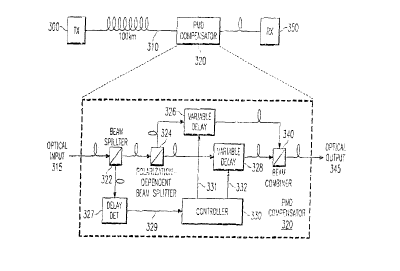
Figure 3A shows a typical end-to-end networl~ path. A transmitter
300 transmits an optical data signal through an optical fiberi310
for detection by a receiver 350. For example, transmitter 300 can
be a DFB laser modulator or any other type of modulated light
source for producing an optical data signal. Optical fiber 310 is a
long-haul, single-rnode, dispersion-shifted fiber approximately one-
hundred kilometers in length. More generally, any type of optica
fiber can be used. Addi~ional fibers, line amplifiers, andlor
repeaters can also b~- included between the transmitter 300 and
I(J receiver 350. Receiver 350 c~n be any suitable photodetector for
detecting the modulated optical data signal.
A polarization-mode dispersion (PMD) compensator 320 is
provided along optical fiber 310 near the receiver 350. According
to the present invention, the PMD corbpensator 320 equalizes PMI)
which further increases bandwidth and transmission range. For
example, given the presence of PMD compensator 320, transmitter
300 can transmit modulated laser data on the order of one to one-
hundred Gb/s (gigabits/sec), or more, over a one-hundred km.
20 single-mode fiber without symbol confusion. Receiver 350 can
detect the output reliably and accurately in a telecommunication
envlronment.
Figure 3B shows a block diagram of the components of the PMD
2s compensator 320 in accordance with one embodiment of the
present invention. Optical paths are indicated generally by a loop
. .
CA 02252775 1998-10-23
WO 98/37645 PCT/US98/03668
- 12-
along the transmiSC;ion path. The optical data signal traveling
through optical fiber 310 enters beam sp~itter 322 as opticai input
315. A portion of the optical input 315 is diverted to a delay
detector 327. The (1elay detector detects delays between two
s orthogonal polarization modes of the detected light. The operation
and implementatiorls of such delay detectors is well-known and
need not be described in further detail.
The majority of the optical input 315 passes through bearn splitter
o 322 to a polarization-dependen~ beam spliiLel- 32~. Th ~
polarization-dependent beam splitter is a type of polariza~ion mode
separator which separates the optical input 315 into two optical
signals that are or~logonally polarized with respect to one another.
The t~,vo polarized signals travel along two separate paths leading
- l5 through respective v ariable switching delay elements 326 and 328.
Each of the variable switching delay elements 326 and 328
provides a respective incremental delay to optical signals passing
therethrough to equalize or compensate for PMD. After passing
through the delay elements 326 and 328, the t~,vo orthogonally
20 polarized optical signals are recombined by beam combiner 340.
An optical output 3~5 having little or no polarization-mode
dispersion is then returned to optical fiber 310 and/or receiver
350.
2s The degree of incremen~al delay, if any, imparted by the variable
switching delay elernents 326 and 328 is manipulated by control
,
CA 02252775 1998-10-23
WO 98/37645 PCT/US98/03668
- 13-
signals received over respective control lines 331 and 332 from a
controller 330. Controller 330 receives data output from thë delay
de~ector 327 representing the m~gnitude of PMD over an output
line 329. Controller 330 then processes the data and generates
5 control signals for the variable switching delay elements 326 and
328 to counteract the PMD effects of the long transmission path
along fiber 310. In particular, the controller 330 sets optical
switches within the variable swi-ching eiemenls ~2b and 328 to
apply an increment~ll relative propagation delay between the
lO orthogonally polar~zed signals which comp~nsates for the delay
detected by delay detector 327. Because PMD is compensated
through optical switching, an extremely fast response time to
detected delay, e.g., on the order of nanoseconds, can be achieved
that is independent of the degree of delay adjustment.
s
Note that in Figure 3B~ two delay elements are applied so that
either polarization can be retarded with respect to the other.
Another variation can use a single delay element to provide a
relative propagation delay. Also, one or more rotatable polarizers
20 can be used at the polarization beam splitter 324 to select a
polarization component at any degree of rotation as the two optical
signals passing through the switching delay elements 326 and 328
do not necessalily have to be orthogonally polarized.
An important feature in accordance with a preferTed embodiment
is the implementation of the variable switching delay elements 326
CAo22527751998-10-23
W098/37645 PCT~S98/03668
-14-
and 328. Each of these switching delay elements have a similar
structure and operation. Accordingly, only one switching tlelày
element need be desc ribed in detail.
Figure 4 shows a detailed example of one variable switching delay
element 426 used in the present invention. A series of optical
switches SWO-SW6 are connected in stages bv different
incremental lengths of fiber. At each stage, an optical switch SWO-
SW6 can switch an optical signal over a reference flber segment or
o a delay flber segment which is longer than the reference fiber
segment so as to introduce an incremental propagation delay.
Depending upon hov~ each switch SWO-~W6 is set, an optical
output 427 can be delayed by different incremental time intervals.
S For example, switch SWO is a 2 X 2 optical cross-connect switch
having four ports A to D. In one switch configuration, switch SWO
can simultaneously connect port A to port C and connect port B to
port D. Optical input 425 would exit port C and travel along a
reference fiber segment 440 experiencing no relative propagation
20 delay, e.g., O picoseconds. Alternatively, SWO can switch optical
input 42~; to pass from port A to exit port D for transmission over
a delay fiber segment 441. The delay fiber segment 441is longer
than the reference fiber segment 440 by a predetermined amount
calculated to introduce a one picosecond propagation delay
25 compared to the transit time for light traveling through the
reference fiber segment 440.
CA 02252775 1998-10-23
WO 98137645 PCT/US98/03668
- 15-
As shown in Figure 4, the switching stages introduce progressively
more delay. In particular, the arrangement of ~igure 4 uses delay
values that progress geometrically by powers of two from one to
s thir~J-two picoseconds for the individual stages. However, the
s-vitching delay element 426 can represent any integral number
delay value from zero picoseconds to sixty-three picoseconds by
valying the switched state of the optical switches SWO-SW6. Many
other value assignments for the propagation delay are certainly
possible and have been contemplated. The use of many low
picosecond values is preferred for high data rate communications
because the stepwis~ introduction of large delay values can cause
momentary signal disruption.
15 Thus, the above propagation delays in the switching delay element
426 are illustrative and can be varied by adding more or less
stages and changing the reference fiber lengths. Further, at each
switching stage, other optical delay elements can be used in
combination with or instead of the optical delay segments to apply
20 a propagation delay. Also, multi-port cross-connect switches
having more than two ports on a side, e.g., N X N optical cross-
connects where N = ~, 4, 8, or more, can be used to allow multiple
delay fiber segments to introduce a greater variety of incremental
delays at each stage.
CAo22527751998-10-23
W098/37645 PCT~S98/03668
- 16-
Each of the optical switches SWO-SW6 is controlled through
control lines 435 bc~sed on a control input 431 output from
controller 330 to se~ a desired propagation delay. A further
optional delay switch controller 433 is included in Figure 4 to
simplify the control task for an external controller 330. Delay
switch controller 433 accepts a relatively simple control input 431,
such as, a reques~ for a particular propagation delay time or a
command to increment or decrement a delay time. In response to
control input 431,delay switch controller 433 then coordinates
o the actions of the individual switches SWO-SW6 so as to
accommodate the request. This might be useful to implement a
standard interface to a wide range of variable delay devices.
Alternatively, the functionality of the delay switch controller 433
can be incorporated in the external controller 330.
Several possible constructions of the individual 2 X 2 optical
switches SWO to SW6 are shown in Figures SA to SD. Figure 5A
shows one 2 X 2 switch 500 having four Semiconductor Optical
Amplifiers (SOAs) 502, 504t 506 and 508 at each port A to D
20 respectively. A 3db (loss) coupler 505 interconnects optical paths
between the pair of SOAs502,504 and the pair of SOAs506 and
508. Asiswellknown, these optoelectronic SOA devices can
provide optical gain ~md switching capability by adjusting the
electrical bias current at a gate that drives the Aevices. For
25 example, ifSOA 502is biased "on," an optical signal at port A can
pass through SOA 502 to 3db coupler 505. The optical signal may
CA 02252775 1998-10-23
WO 98t37645 PCT/US98/03668
- 17-
be further switched (and amplified~ to e~;it port C and/or D ~ith
little or no loss by turning on SOA 506 and SOA 508 respectivelv.
Another 2 X 2 switch variation is shown in Figure 5B having four
s couplers 523, 525, 527 and 529 at each port A to D to form four
optical paths cross-connected between the ports A to D. Four
SOAs 522-528 are provided for switching and amplifying optical
signals passing along the four optical paths. Although more
couplers are used, this configuration has the advantage that A-D
o and B-C connections are possiDie withou~ mixing optical signals
input at ports A ancl B.
Figure 5C shows a further variant that separates switch 500 into
two half-switches 5f~0 and 560. Half-switch 540 has two SOAs
542, 544 at ports A and B connected to a 3db coupler 545. Half-
switch 560 has t~vo SOAs 566 and 568 at ports C and D
connected to a 3db coupler 565. The two 3bd couplers 545 and
546 optically couple the two half-switches 540 and 560. A stage
with such a half-switch at either end forms a modular unit. This
can be useful from a design and implementation standpoint. As
with thte other switch designs, this arrangement can be made
lossless by using the SOAs 542, 544, 566 and 568 to provide
some gain.
2~ Finally, Figure 5D shows a switch 580 having well-known Mach-
Zehnder electro-optic switches 582 and 586 to route the optical
CA 02252775 1998-10-23
WO 98/37645 PCT/US98/03668
- 18-
signals between ports A to D under the influence of electrical fieid
gradients. A f~xed gain block 584, such as, an optical ar~plifier, is
added to compensa~e for any inherent coupling loss of ~he Mach-
Zehnder switches 582, 586.
-
Figure 6 is a block diagram or a PMD simulator in accordance witha preferred embodiment. As described above, since light si~nals
~ransmitted through a single mode fiber experience polanzation
that is best described in te~ s of a horizontal component and a
vertical component, each component travels on a path normal to
the a~is of light propagation. The transmission of these signal
components is affected separately by causing them to be less than
perfectly synchronized. This problem is referred to as Polariza~ion-
Mode Dispersion (PMD). PMD results in broadened signals that
s are difficult for a receiver to properly read and interpret. Thus,
there exists a requirement to test the ability of various receivers to
withstand the effect of PMD and keep signals within the limits of
the receivers.
20 Figure 6 illustrates such a solution. The PMD simulator illustrated
in Figure 6 receives a beam of optical light at the Polarization
Beam Splitter (PBS) 600 and splits the beam of light into a pair of
signals TE 610 and TM 620. The signals are diverted to individual
variable time delay elements 630 and 631. The arnount of delay is
2s controlled by a time variant controller 650 to introduce the
appropriate amount of delay to optimize the perforrnance and
_ _
CA 02252775 1998-10-23
WO 98137645 PCT/US98/03668
- 19'
compensation to the effects of PMD. Then, the signals are joined
at the polarization beam joiner 640 witll appropriate compen~ation
having been achieved. One of ordinary sl~ill in the art will readily
comprehend that the variable time delay elements can utilize any
of the techniques discussed herein or any other technique to
introduce the appropriate amount of delay into the system.
In another embodiment of the invention, the simulator system
brealis the signal into at least two polarization modes, and inserts
o variable time delay elements into each of the paths as described
above. Then, the artificial PMD signal is sent to a receiver, and the
controller 650 varie~ the frequency and the amount of dispersion
that each of the rnocles have as they come out of the fiber. A
number oi receivers are Utestedn using the same test pattern
resulting from the controlled modes to compare perforrn~nce and
maintain uniformity of the signal. The simulator can also be used
to maintain quality control, for example, by gathering time-variant
dispersion data from a computer on the network and using this
data in the simulation controller 650 to test the other circuits
20 against an actual measurement.
The present invention is described in the exarnple environment of a
fiber communication network. Description in these terrns is
provided for convenience only. It is not intended that the invention
2~ be limited to application in this exarnple environment. In fact,
after reading the following description, it will become apparent to a
CA 02252775 1998-10-23
WO 98/37645 PCT/US98/03668
- 20 -
person skilled in the relevant art how ~o implement the invention
in alternative environments.
While various embodiments of the present invention have been
s described above, it should be understood that they have been
presented by way of example only, and not limitation. It will be
understood by those skilled in the art that various changes in form
and details may be made therein without departing from the spirit
and scope of the invention as defined in the appended claims.
o Thus, the breadth and scope of the present invention should not
be limited by any of the above-described exemplar~ embodiments,
but should be defined only in accordance with the following claims
~nd their equivalents.