Note: Descriptions are shown in the official language in which they were submitted.
CA 02252887 2001-O1-25
BACKGROUND OF THE INVENTION
The use o. removable, self-contained electronic devices,
such as flash memory cards, is known. Such devices offer
advantages because of their relatively convenient size, typical
plug and play compatibility and ease of removal, among other
things. Such devices may be used, for example, in digital
cameras. However, these advantages are dependent on providing
reliable electrical connection between the removable device and
the hos~ device. It is therefore desirable to have a reliable
and easy to use interface device for connecting removable devices
to host devices.
BRIEF SUMMARY OF THE INVENTION
In accordance with the present invention, a miniature card
docking connector includes an interface connector and a frame
which are mounted on a printed circuit board. The frame is
formed to partially enclose the interface connector and a
miniature card. In particular, the frame includes an overhang
wall which secures the forward portion of the miniature card.
A resilient latch mechanism facilitates securing the miniature
2o card within the frame. The latch mechanism includes two
retaining members connected to a release mechanism that can be
pressed to release the miniature card from the frame, and may be
CA 02252887 1998-10-21
WO 98/39695 PCT/US98/03180
-2-
either formed as part of the latch mechanism or as a seperate
piece. The frame includes a plurality of pilot retainers with
latches disposed thereon for initially locating the frame
relative to pre-drilled holes in the printed circuit board. In
particular, the pilot retainers are inserted into the pre-drilled
holes such that the latches on the pilot retainers secure against
the opposite side of the printed circuit board relative to the
frame. Integral, threaded nut portions are provided in the frame
to facilitate more secure connection of the frame to the printed
circuit board by means such as bolts.
The interface connector functions to connect the miniature
card to a host device and includes an elastomeric connection
device having top and bottom surfaces and electrical contacts
which provide an electrical pathway between the top and bottom
surfaces; and an insulating body with an opening adapted to
receive the elastomeric connection device, the insulating body
being further adapted to be received by the host and to receive
the miniature card such that the elastomeric connection device
provides electrical connection between corresponding electrically
conductive pads on the miniature card and the host. The
insulating body also includes a castellated sidewall disposed
around the elastomeric connection device. The castellated
sidewall shields the elastomeric connection device from foreign
objects which might be inserted into the connector. The
insulating body may also include an alignment feature for
facilitating proper alignment of the connector with regard to the
host device, and a keying feature for preventing connection of
incompatible miniature cards to the host.
The present invention provides advantages related to both
reliability and size. Improved reliability is provided by
employing the elastomeric connection device rather than a
traditional pin and socket type connector. The elastomeric
connection device offers multiple contact points and multiple
conductive paths for each connection. Further, the elastomeric
connection device is rugged and does not use fragile pins which
may bend or break when placed under strain. The interface
CA 02252887 1998-10-21
WO 98/39695 PCT/US98/03180
-3-
connector and miniature card of the present invention are also
smaller in size than corresponding PCMCIA components, and thus
offer advantages normally associated with smaller size.
Additionally, the interface connector and miniature card are well
suited to use with modern flash memory components.
Various types of location pins may be used to provide secure
alignment between the interface connector and the host device.
More particularly, the interface connector may include pins with
diamond-shaped cross-sections sized to fit into circular holes
in the host device. An interference fit is provided because two
point-contact edges of each pin contact sidewalls of the
corresponding hole. Alternatively, the pins may have circular-
shaped cross-sections and include radial ribs to provide a
plurality of contact points when inserted into the hole. These
designs provide positive alignment with increased tolerance for
manufacturing process variations prior to insertion.
The keying feature of the present invention prevents
incompatible miniature cards from being connected to the host.
More particularly, the interface connector may employ an insert
having at least one tab portion extending toward the miniature
card. When a compatible miniature card is inserted, gaps on the
miniature card mesh with the tabs on the insert, thereby allowing
the miniature card to be connected to the host. However, when
an attempt is made to insert an incompatible miniature card, the
tabs on the insert physically block the non-matching gaps on the
incompatible miniature card, thus preventing connection.
Different inserts having different tab configurations can be
employed for different types of miniature cards. The keying
feature can be advantageously used to prevent damage which might
be caused by voltage mismatches, such as from inserting a +3V
powered miniature card into a +12V supplying host.
BRIEF DESCRIPTION OF THE SEVERAL VIEWS OF THE DRAWING
The invention will be more fully understood from the
following Detailed Description and the Drawing, in which:
CA 02252887 1998-10-21
WO 98/39695 PCT/US98/03180
-4-
Fig. 1 is a perspective view of a miniature card interface
connector in accord with the present invention;
Fig. 2 is a plan view of the interface connector of
Fig. 1;
Fig. 3 is a front view of the interface connector of
Fig. 1;
Fig. 4 is a side view of the interface connector of
Fig. 1;
Fig. 5 is an exploded view of the interface connector in
relation to a miniature card and host;
Fig. 6 is a perspective view of the bottom of the interface
connector and frame of Fig. 5;
Fig. 7 is a perspective view of a high profile interface
connector;
Fig. 8 is a plan view of the high profile interface
connector;
Fig. 9 is a front view of the high profile interface
connector;
Fig. 10 is a side view of the high profile interface
connector;
Fig. 11 is an exploded perspective view of the interface
connector illustrating the horizontally deflecting power/ground
contacts;
Fig. 12 ,is a perspective view of the horizontally deflecting
power/ground contacts;
Fig. 13 is a side view of the horizontally deflecting
power/ground contacts;
Figs. 13a-13c further illustrate features of the
power/ground contacts of Figs. 12-13;
Figs. 14 is a top view of an interface connector having
vertically deflecting power/ground contacts;
Fig. 15 is a cross sectional view of the interface connector
of Fig. 14 and the miniature card taken along line 1-1;
Figs. 16-19 further illustrate vertically deflecting
power/ground contacts;
Figs. 20-21 illustrate the write-protect feature;
CA 02252887 1998-10-21
WO 98/39695 PCT/US98/03180
-5-
Figs. 22-24 illustrate the keying feature;
Figs. 25-30 illustrate location pins;
Fig. 31 is a top view of an alternative frame;
Fig. 32 is a side view of the frame of Fig. 31;
Fig. 33 is a bottom view of the frame of Fig. 31;
Fig. 34 is a cross-sectional side view of the frame of Fig.
31 taken along line 5-5, which illustrates the latch prior to
insertion of the miniature card;
Fig. 35 is the cross-sectional view of Fig. 34 illustrating
the latch after insertion of the miniature card;
Fig. 36 is a top perspective view of a low-profile, multi-
piece frame;
Fig. 37 is a plan view of the multi-piece frame of Fig. 36;
Fig. 38 is a cross-sectional view of the frame of Fig. 37
taken along line 6-6; and
Fig. 39 is a bottom view of the frame of Fig. 37.
DETAILED DESCRIPTION OF THE INVENTION
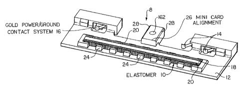
Fig. 1 illustrates an interface connector 8 for use with a
host and a miniature card. The interface connector includes an
elastomeric connection device 10, an electrically insulating body
12, ground contacts 14 and a power contact 16. The elastomeric
connection device 10 extends through the insulating body 12 and
includes an elastomeric insulator 18 and one or more rows of
independent conductive contacts 20 situated therein. The
conductive contacts extend through the elastomeric insulator, and
thus through the insulating body.
Referring to Figs. 1-4, the insulating body 12 includes an
opening 21 (See also Fig. 11) which extends through the
insulating body and is adapted to receive the elastomeric
connection device 10 and allow the upper and lower surfaces of
the elastomeric connection device to connect with a miniature
card and host, respectively. The opening is crowned by a side
wall 22 which includes a plurality of castellations 24. The
opening has a width dimension which is smaller than a
characteristic (non-deflected) width dimension of the elastomeric
CA 02252887 1998-10-21
WO 98/39695 PCT/US98/03180
-6-
connection device prior to insertion into the opening. As such,
frictional force between the castellated side wall and the
elastomeric connection device operate to secure the elastomeric
connection device in place, and thus prevent the connector from
falling out of the opening. Alternatively, the elastomeric
connection device may be secured in place with an adhesive or
other means known in the art.
The castellated side wall 22 is employed to support the
elastomeric connection device 10 and to decrease the likelihood
of foreign objects coming into contact with the elastomeric
connection device. The castellations are separated by gaps. The
miniature card may include a corresponding castellated wall with
castellations which, when the miniature card is properly aligned
with the interface~connector, interface with the interface
connector gaps such that the miniature card castellations do not
physically contact interface connector castellations.
The interface connector may include an alignment feature
such as a post 26 for facilitating proper alignment of the
miniature card with respect to the interface connector. The post
is disposed centrally on the interface connector and is formed
as part of the insulating body. The post includes beveled edges
28 and is shaped to snugly interface with a cutaway section on
the miniature card.
Figs . 5-6 illustrates the interface connector 8 in relation
to a host device 30 and a miniature card 32. The host includes
a frame 34, a printed circuit board ("PCB") 36 and a backup plate
38. The PCB is sandwiched between the backup plate and the
frame, which are secured by bolts of other suitable means.
The frame 34 is formed to receive the miniature card after
receiving the interface connector. More particularly, the frame
and the PCB form a recess into which the miniature card is
securely placed. The miniature card includes a forward portion
39 which fits between the interface connector and the frame.
Contacts which correspond to ground and power contacts on the
interface connector are disposed on the forward portion of the
miniature card. The miniature card also includes a PCB having
CA 02252887 1998-10-21
WO 98/39695 PCT/US98/03180
one or more rows of electrically conductive pads corresponding
to the contacts of the elastomeric connection device. The host
device similarly includes a PCB with corresponding power and
ground contacts, as well as rows of electrically conductive pads
for transmission of signals through the elastomeric connection
device. A rear portion of the miniature card includes at least
one surface which is secured by a latch 40 in the frame when the
miniature card is inserted therein.
Electrical connections other than power and ground e.g.,
data lines, are provided via the elastomeric connection device
10. Typically, both the host 30 and the miniature card 32
include PCBs with rows of corresponding connection pads.
Corresponding pads must be placed in electrical communication for
proper operation. When the interface connector is inserted into
the host, the lower surface of the elastomeric connection device
deflects against the host pads. When the miniature card is
subsequently inserted into the frame, the upper surface of the
elastomeric connection device deflects against the miniature card
pads. The host and miniature card are thus placed in electrical
communication, and a PCB to PCB connection is provided through
the elastomeric connection device.
The interface connector provides connection between the
miniature card and interface device in a manner which is
conducive to plug and play functionality. Because the
castellated sidewall 22 is raised above the surface of the
insulating body 12 , the miniature card must be inserted in an
angular fashion. When the miniature card power and ground
contacts are pressed against the interface connector power and
ground contacts 16, 14, the miniature card can then be pivoted
downward until the corresponding rows of pads on the miniature
card and host are in electrical communication, and the miniature
card is secured in place by the latch 40. Thus, the miniature
card power and ground contacts enter electrical communication
with the host device before the data lines, as is desirable for
plug and play functionality.
CA 02252887 1998-10-21
WO 98/39695 PCT/US98/03180
_g_
In order to provide an indication when a miniature card is
inserted into the frame 34 , a final detect contact 41 may be
employed. The final detect contact is a metal beam with two high
points. The contact 41 is heat staked to the plastic latch 40,
and moves therewith as miniature cards are inserted into and
removed from the frame. When the frame is mounted on the PCB 36
the high points of the final detect contact deflect against the
surface of the PCB. Pads disposed on the PCB surface are
employed to detect the position of the contact 41, and thus
determine whether a miniature card is present in the frame. For
example, the final detect contact can be aligned to form a short
between the pads on the PCB in the presence of a miniature card
in the frame, and to form an open between the pads in the absence
of the miniature card.
In an alternative embodiment illustrated in Figs. 7-10 the
interface connector is configured for a deeper frame. The high
profile interface connector 8 includes a deeper base 42 which may
be constructed of solid polycarbonate. The base provides
increased height for use with alternative configuration frames
and miniature cards.
The power and ground connectors 16, 14 which electrically
connect the miniature card to the interface connector are
illustrated with greater detail in Figs. 11-13. The power and
ground connectors each include an upper arm section 46 and a
lower arm section 48 which are connected at an intersection 50
surface . The lower arm 48 extends downward from the intersection
50 and is curved away therefrom. The upper arm 46 extends
outward to one side of the intersection 50 and curves away
therefrom such that when the connector is placed in the slot 52
in the insulating body, the upper arm 46 extends out of the slot
52 with sufficient space for deflection, and the lower arm 48
extends below the insulating body with sufficient space for
deflection as the interface connector is secured in the frame.
In operation, the upper arm 46 electrically connects to contacts
on the miniature card by deflecting horizontally as force is
applied thereagainst. The lower arm 48 deflects vertically
CA 02252887 1998-10-21
WO 98/39695 PCT/US98/03180
_g_
against pads on the host PCB. Barbs 120 which extend from the
intersection surface 50 facilitate securing the connector in the
interface connector slot by anchoring against the slot walls.
The connectors may be fashioned from a single piece of conductive
metal by stamping or other suitable techniques known in the art.
Referring now to Figs. 12, 13, 13a, 13b, 13c, the power and
ground connectors have features which facilitate reliable
operation. The upper and lower arms each include an enlarged
contact surface 122, 124 at the respective ends thereof opposite
the intersection 50 surface. The enlarged contact surfaces
provide a relatively large surface area for achieving electrical
connection with corresponding pads on the miniature card and host
PCB, thereby improving reliability. Further, the upper enlarged
contact surface includes an anti-overstress feature. The upper
contact surface 122 includes first and second arcuate edges 126,
128, respectively. To alleviate overstress during deflection,
the first edge 126 has a greater length than the second edge 128.
The upper arm 46 also includes three radii 130, 132, 134 which
deflect at different rates. Further, the slot 52 window through
which the upper arm extends in the interface connector is formed
with a wall 136 to support the first radius 130 during deflection
in order to alleviate overstress and to provide greater contact
force against the corresponding pad on the miniature card PCB.
An anti-overstress surface 138 in the window prevents the upper
arm from being deflected past a given point within the window.
More particularly, the enlarged contact surface 122 contacts the
anti-overstress surface 138 when the upper arm 46 is fully
deflected, and the upper arm is prevented from deflecting further
by the anti-overstress surface which blocks the path of further
deflection.
As illustrated in Figs. 14-19, alternative power 54 and
ground 56 contacts on the interface connector operate to connect
corresponding contacts on the miniature card with contacts on the
host by deflecting vertically against the miniature card and host
device contacts. Each interface connector power and ground
CA 02252887 1998-10-21
WO 98/39695 PCT/US98/83180
-10-
contact 54, 56 is formed from a ribbon-like conductive metal
strip. The contacts 54, 56 include a substantially straight
securing section 58 which is secured to the interface connector
by insertion into the preformed slot in the insulating body. A
host contacting portion 60 of the interface connector contact is
located adjacent to the securing section and is operative to
deflect vertically (upwards) as the interface card is placed in
the host. Downward deflective force maintains contact between
the host contacting portion and the corresponding host contact.
A miniature card contacting portion 62 of the interface connector
contact is located adjacent to the securing section 58. The
miniature card contacting portion is formed into a partial loop
which prevents the contact end from being damagingly jammed into
the miniature card. The miniature card contacting portion 62
deflects vertically downward as the miniature card is inserted
into the interface connector, and deflective force maintains
electrical connection between the contacting portion and the
corresponding pad on the miniature card. It will therefore be
appreciated that the contacts 54, 56 deflect vertically when
contacting both the host pads and the miniature card pads.
As illustrated in Figs. 20-21, the miniature card may
include a write-protect tab 64 for providing selectable write
protection for writable miniature card devices. The interface
connector includes a write-protect contact 66 which is normally
electrically connected to a first host write-protect pad 68,
i.e., the interface connector stays resident in the host. The
write-protect tab 64 operates to control electrical connection
between the first write-protect pad 68 and a second write-protect
pad 70. The write-protect tab 64 is a nonconductive panel which
can be slidably moved to deflect the write-protect contact and
thereby cause the contact to electrically connect with the second
write-protect pad 70. The write-protect tab can also be slidably
moved away from the write-protect tab to un-deflect the contact
66 away from the second write-protect pad 70. Circuitry within
the host can be utilized to prevent writing of data when a
CA 02252887 1998-10-21
WO 98/39695 PCT/(JS98/03180
-11-
predetermined voltage potential is not present at the first
write-protect pad 68.
Referring now to Figs. 22-23, the interface connector may
also include a keying feature for selectively accepting and
rejecting insertion of predetermined types of miniature cards.
It is envisioned that different types of miniature cards may be
configured for different voltage levels. The keying feature
could be employed to, e.g., prevent insertion of a +3V flash
memory miniature card into a host device which is designed for
a +5V flash memory (and provides +5V at the power contacts) . The
keying feature employs an irregularly shaped plastic insert 74
which is shaped to fit in a corresponding irregularly shaped
keyhole 76 in the insulating body. The insert includes a tab
portion 78 which prevents insertion of incompatible miniature
cards. The plastic insert includes a first peg 80 for aligning
and securing the insert in place and a second peg 82 for aligning
and securing the tab 78. The interface connector includes at
least one hole 84 for accommodating tab pegs 82. Hence, a
variety of tab patterns including pluralities of tabs may be
accommodated such that a single design of insulating body can be
customized to accept any of various compatible miniature cards,
while rejecting incompatible miniature cards, by insertion of an
appropriate plastic insert. Gaps on the miniature card
corresponding to the tabs on the interface connector insert 74
would thereafter physically block insertion of incompatible cards
in the same manner as described with respect to the keying
feature 72 above.
Features which facilitate alignment of the interface
connector with respect to the host device are shown in Figs. 25
30. More particularly, the interface connector includes outer
location pins 86 and a center location pin 88 disposed on the
flat bottom surface. The pins have a diamond-shaped cross-
section, and are adapted to interface tightly with corresponding
circular holes in the host. Each location pin includes two
outermost edges 90 which are separated by a length dimension 92
approximately equal to the diameter dimension of the holes. The
CA 02252887 1998-10-21
WO 98/39695 PCT/US98/03180
-12-
pins and holes thereby provide a point contact, interference fit
which provides proper and secure alignment with tolerance within
a predetermined range of dimensional mismatch between the hole
diameter and the length dimension. Such a mismatch could be
caused by manufacturing tolerance variation.
The insulating body 12 may include recesses 94 around the
location pins for accepting waste material produced during
assembly. When the pin is inserted into the hole during
assembly, excess material at the contact point, typically a thin
plastic shaving, is sheared away. In the absence of a recess
such excess material could jam between the interface connector
and the host, thereby inhibiting proper insertion and alignment.
By forming recesses into which the pins are disposed, material
shaved away during insertion of the pin into the hole is
deposited in the recess and thereby does not interfere with
proper insertion and alignment.
The location pins are arranged to inhibit twisting and
shifting of the interface connector relative to the host. More
particularly, the center pin 88 is ninety degrees out of phase
relative to the other pins. The center pin 88 contact points 90
are aligned along a first axis 3-3, and the outer pin contact
points are aligned along parallel axes 5-5, 7-7. This
arrangement provides static positioning relative to the axes 3-3,
5-5, 7-7, and prevents rotation of the interface connector around
the center pin 88.
Alternative shapes for the location pins may also be
utilized. As shown in Fig. 29, alternative pins 96 may have a
circular cross-section and include a plurality of radial ribs.
Each radial rib can potentially form a point contact 98. Thus,
greater tolerance for manufacturing process variation may be
realized with an associated possible increase in force required
to insert the pin into the hole. In another alternative
embodiment shown in Fig. 30, five location pins are utilized.
A center location pin 100 is oriented along a first axis 9-9 and
outer location pins 102, 104, 106, 108 are oriented along
parallel axes 11-11, 13-13, 15-15, 17-17, respectively, which are
CA 02252887 1998-10-21
WO 98/39695 PCT/US98/03180
-13-
perpendicular to the first axis 9-9. Further, the location pins
include bevelled point contact edges 110 which facilitate
insertion of the interface connector into the host.
Figs. 31-33 illustrate an alternative frame 140. The frame
140 includes two opposing sidewalls 142, a forward wall 144 and
a rear wall 146. A printed circuit board ("PCB") pilot retainer
148 is disposed at the midpoint of each sidewall 142. Each pilot
retainer 148 extends downward from its respective sidewall 142
and includes a latch 150 disposed at a distal end thereof
relative to the frame 140. The forward wall 144 includes three
protrusions, each having a respective threaded insert 152. An
overhang wall portion 154 is disposed on the upper forward
sidewall 144 such that the miniature card connector 8 is
partially shielded from above once inserted into the frame. The
rear wall 146 includes two threaded inserts 152 at distal ends
thereof and a latch 156.
To mount the frame on a printed circuit board, pilot holes
158 are first drilled in the printed circuit board corresponding
to the desired location of the pilot retainers 148. The frame
is then placed vertically onto the printed circuit board such
that the pilot retainers 148 are inserted into the respective
holes 158 corresponding thereto . The latches 150 disposed on the
distal ends of the pilot retainers deflect upon such insertion,
and subsequently secure to the underside of the printed circuit
board 36 when inserted fully therethrough. Bolts are then
inserted through the holes in the PCB and connected to
corresponding threaded inserts to more securely mount the frame
on the printed circuit board.
A multi-sided post 160 is disposed on the forward wall 144
for securing the interface connector 8 in the frame while the
frame is being mounted on the printed circuit board. More
particularly, a multi-sided post 160 extends downward from the
center of the overhang portion 154 of the forward wall. The post
160 is sized to form a press fit when inserted into an
appropriately sized hole 162 (Fig. 1) disposed in post 26 (Fig.
1) of the interface connector 8. Hence, the interface connector
CA 02252887 1998-10-21
WO 98139695 PCT/US98/03180
-14-
is retained against the frame while the frame is inverted and
mounted on the printed circuit board.
Locating posts 157 may be provided on the interface
connector for assuring proper alignment and connection with the
printed circuit board. Once the frame is mounted on the printed
circuit board, the interface connector is sandwiched between the
frame overhang portion 154 and the surface of the printed circuit
board 36, with post 160 preventing the interface connector from
moving laterally outward from between the overhang portion and
printed circuit board. Further, a plurality of locating posts
157 are disposed on the lower surface of the interface connector
to align the interface connector with pre-drilled holes 159 in
the printed circuit board, and provide mechanical connection
thereto. The posts 157 are multi-sided, with diamond-like cross-
section and a diameter slightly larger than the holes 159.
Hence, the posts 157 provide a press fit into the holes 159 to
securely hold the interface connector in place on the printed
circuit board.
Referring to Figs. 31-35, the latch 156 includes two base
members 164 and a crossbar 166 which is disposed therebetween and
interconnects the base members. The base members 164 are
anchored to the rear wall 146. A curved spring member 168
extends inward from each base, and is terminated by a latching
member 170. The outer edge of the latching member 170 is beveled
to facilitate insertion of the miniature card 32 by causing the
spring members 168 to gradually deflect as the miniature card is
inserted into the frame. A lower, securing edge of each latching
member 170 is located at a height position within the frame
corresponding to a securing edge of a fully inserted miniature
card 32. When the miniature card securing edge is below the
latching member securing edge, the force of the spring member
moves the latching member toward the miniature card and over the
miniature card securing edge, thereby securing the miniature card
within the frame.
The latching members 170 are connected by the crossbar 166,
thereby facilitating release of the miniature card 32 from the
CA 02252887 1998-10-21
WO 98/39695 PCT/CTS98/03180
-15-
frame. In particular, a gap is formed between the crossbar and
the rear wall such that the crossbar can be moved toward the rear
wall by application of force. When such force is applied to the
crossbar the latching members are moved toward the rear wall
until the latching edge moves laterally beyond the securing edge
on the miniature card and the miniature card is released from the
frame. In order to facilitate application of force to the
crossbar, the crossbar is formed with a curvature which leaves
a gap between the crossbar and the fully inserted miniature card.
The tip of a person's finger or other small object may then be
partially inserted into the gap in order to apply force to the
crossbar and release the miniature card.
To further facilitate release of the miniature card from the
frame, spring-like force is constantly applied to the forward
portion of the miniature card when the miniature card is secured
in the frame. More particularly, when the miniature card is
rotated into the frame, pressure is applied to the forward
portion of the miniature card by the overhang portion of the
forward wall and elastomer of the interface connector. Such
pressure slightly deflects the overhang portion and elastomer
such that upon release of the latching members the elastomer and
overhang portion return to their original respective positions
and thereby force the miniature card to pop upward out of the
frame. Hence, it is not necessary to pry the miniature card out
of the frame and thereby risk damage.
A low-profile, multipiece frame is illustrated in Figs. 36-
39. A docking port 172 is employed for mounting of a separately
formed interface connector assembly 8 and latch mechanism 174.
The interface connector 8 is mounted on the docking port 172 by
a press fit between multi-sided post 160 and hole 162, as
described above. The latch mechanism 174 snaps into a receiving
portion of the docking port, and is secured thereto by posts 178.
In particular, the posts 178 are terminated with inward facing
hook portions which secure under opposing sides 180 of the latch
174 when the latch is fully inserted into the receiving portion
of the docking port.
CA 02252887 1998-10-21
WO 98/39695 PCT/US98/03180
-16-
The latch 174 is slidably movable once mounted on the
docking port 172. The latch 174 includes two guideposts 182
which fit into guideslots 184 formed in the docking port 172.
The guideposts and guideslots allow limited, forward-rearward
sliding motion of the latch, and prevent lateral and twisting
motions. A flexible, curved spring member 186 is formed on the
latch with two spring arms and a base portion disposed
therebetween. The spring member 186 contacts the rear wall 146
of the docking port and thereby maintains the latch fully
extended toward the center of the docking port, to the extent
allowed by the guideposts and guideslots. When a miniature card
is inserted into the docking port, the rear portion of the
miniature card contacts beveled latch members 188 on the forward
edge of the latch, and causes the latch to move toward the rear
wall 146 of the docking port as the spring member is deflected.
When the miniature card is fully inserted into the docking port
the latch members extend over the top of the miniature card, held
by the force of the spring member 186, thereby securing the
miniature card within the docking port. A raised curvature 190
is disposed on the latch 174 to facilitate removal of the
miniature card from the docking port by sliding the latch toward
the rear wall 146 with a person's finger until the latch members
no longer secure the miniature card.
It should be understood that the invention is not limited
to the particular embodiments shown and described herein, and
that various changes and modifications may be made without
departing from the spirit and scope this novel concept as defined
by the following claims.