Note: Descriptions are shown in the official language in which they were submitted.
CA 022~2920 1998-10-23
WO97/41665 PCT/SE97/00665
D.T.R.M DATA TIMING RECOVERY MODULE
TECHNICAL FIELD OF THE lNV~:N~lON
The present invention relates to a data timing recovery module
for clock recovery, more particular to clock extraction.
DESCRIPTION OF RELATED ART
Clock recovery is a well known method to recover timing on a
signalling link. The simplest way to send data on a serial
o electrical link is to use two different physical connections,
one for data and one for timing, clock. One of the connections
can be avoided by extracting the timing information from the
data by means of a special code, for example CMI, HDB3, AMI
etc. By using one of these transmission codes, the normal data
bandwidth will be differently distributed and some high
frequency components will be generated. These components are
used to extract the timing information. This procedure is
called "clock recovery."
By using one of the previous codes the data bandwidth will be
enlarged. Because of that, it will be necessary to increase the
transmission media performance, and consequently more
expensive. This problem has been solved by using codes that
preserve the bandwidth characteristics, but the timing recovery
operation is more difficult. Circuits normally used for the
clock extraction need one or more data transitions every few
bit group, or the clock could not be extracted. The code used
must guarantee this condition, e.g. non-return to zero (NRZ)
scrambled data. The clock extraction problem is easily solved,
especially if the data pattern used is poor of transitions.
CA 022~2920 1998-10-23
W O 97/41665 PCTISE97/00665
There are two existing methods to realize the clock extraction
from an NRZ scrambled data link:
The first method consists of a narrow band phase locked loop
(PLL), circuit with a digital phase comparator that
continuously measures the phase difference between the positive
(or negative) data transition and the clock edges which are
generated by a local oscillator. The frequency of this
oscillator will be adjusted so as to eliminate the phase
difference between data transitions and clock edges. This is an
expensive solution because often it is difficult to implement
by standard discrete components. Furthermore, the flexibility
is limited using this method because all the physical
parameters such as frequency, pattern, etc. cannot be changed
to cover other possible re~uirements.
The second method to extract the timing information consists of
the application of a Q tank followed by a high gain selective
amplifier stage. The Q tank is realized by a simple LC circuit,
or by using a SAW resonator, continuously stimulated from data
edges transitions. If a LC resonator is used, a special
inductor is needed in order to have a sufficiently large Q
value to preserve the timing information during long "O" or "l"
sequences. This is a more flexible solution, but it has lower
performance than the one described previously. The recovered
clock, for example, is affected by jitter because the S/N ratio
is very low at the Q tank output, especially if the pattern
used is poor of transitions.
JP 88-174442 by Masushita et al, have an oscillator in free
running mode to guarantee a timing clock at the output XXX. The
invention is to suppress the appearance of noise and jitter in
CA 022~2920 1998-10-23
WO97/41665 PCT/SE97/0~65
a periodical reproduction output, by obtaining a required
timing clock based on self-advancing oscillation.
S~RY
One problem this invention solves is to extract a clock signal
at high rate.
Another problem this invention solves is to preserve the timing
information during long "0" or "l" sequences.
This invention solves the clock recovery problem in a new way
by using a known effect which was originally used for another
purpose. The purpose was for frequency modulation receivers,
carrier modulation systems and to multiply or divide a clock
lS frequency by an integer number.
The present invention is a data timing recovery system, i.e. a
data timing recovery module (DTRM), which is based on an injec-
tion locked oscillator, ILO. This invention extracts the timing
information from a high bit rate data signal, e.g. scrambled
NRZ coming from optical or electrical interfaces. Other data
patterns than NRZ can be used. The timing recovery system uses
a lock-in phenomena in the ILO. The timing information will be
extracted even if the data stream is composed by long sequences
of bit logic level "l" or by long sequences of bit logic level
~o~ repeatedly. At every data transition event, a zero crossing
circuit generates a pulse which is used to phase lock the
frequency generated by the oscillator.
This invention has at least two parts; the pulse generator
circuit, and the injection locked oscillator. Other parts that
~ .
CA 022~2920 1998-10-23
WOg7/41665 PCT/SE97/00665
can be used are a clock extractor circuit including the ILO, a
phase aligner circuit and a clock killer circuit.
One advantage is that the DTRM can extract time information
from high Mbit/s signals at a low cost.
Another advantage is that the DTRM can extract time information
from high Mbit/s signals at high performance.
Another advantage is that the DTRM can be made to be very small
in its dimensions.
Yet another advantage is that the DTRM is easy adaptable to
different bit rate operation.
The invention is now being described further with the help of
the detailed description of preferred embodiments and attached
drawings.
BRIEF DESCRIPTION OF THE DRAWINGS
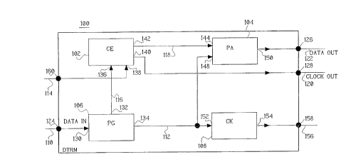
Figure l shows a block diagram of a data timing recovery
module, DTRM.
Figure 2 shows a pulse generator circuit (PG).
Figure 3 shows a clock extractor circuit (CE).
Figure 4 shows a phase aligner circuit (PA).
Figure 5 shows a clock killer circuit (CK).
Figure 6a shows the block diagram of an ILO.
Figure 6b shows the working principle of the ~LO.
Figure 7 shows a time relating flow chart for an incoming data
signal which goes into the DTRM, which produces phase aligned
data and recovered clock signals.
CA 022~2920 1998-10-23
WO97/41665 PCT/SE97/00665
Figure 8 shows a signal diagram over different signals in the
DTRM.
Figure 9 shows an alternative embodiment of the DTRM.
5 DET~Tr~n DESCRIPTION OF EMBODIMENTS
A more detailed description of the present invention will
hereby be presented.
The present invention relates to a clock recovery circuit for
o telecommunication equipment. This circuit can be used in other
applications as well, where clock recovery is needed for high
speed transmission links.
A short description of the drawings will be presented.
Figure 1 shows a block diagram of a data timing recovery module
100, DTRM. The four blocks include; a clock extractor circuit
102, CE, i.e. a pulse controlled oscillator circuit (PCO), a
phase aligner circuit 104, PA, a pulse generator circuit 106,
PG, and a clock killer circuit 108, CK. These blocks are
connected to each other by physical links. The data timing
recovery module 100 has two incoming data links; the first
incoming link being an incoming data link 110, carrying
incoming data, connected to an incoming data link input 124,
and the second incoming link being an enable/disable link 114,
carrying an external clock disable signal, connected to an
incoming clock disable input 160. The DTRM 100 also has three
outgoing links; the first outgoing link being an outgoing data
link 122, carrying phase aligned data, connected to an outgoing
data link output 126, the second outgoing link being an
outgoing clock link 120, carrying first recovered clock,
connected to an outgoing clock link output 128, and the third
CA 022~2920 1998-10-23
WO97/41665 PCT/SE97/00665
outgoing link being a loss of signal link 156, carrying a data
loss signal, connected to a loss of signal output 158.
The pulse generator 106 has an incoming link being the incoming
data link 110, connected to an incoming data link input 130 yia
the incoming data link input 124 of the DTRM lO0. The pulse
generator 106 also has two output links; the first output link
being a pulse link 116, carrying pulses, connected between a
pulse link output 132 and to a pulse link input 136 of the
o clock extractor 102, the second output link being a data link
112, carrying data, connected to a data link output 134 and to
a data link input 152 of the clock killer 108. The data link
112 is also connected to a data link input 148 of the phase
aligner 104.
~5
The clock extractor 102 has two incoming links; the first
incoming link being the enable/disable link 114 connected to an
enable/disable link input 138 via the incoming clock disable
input 160 of the DTRM 100, and the second link being the pulse
link 116 connected to the pulse link input 136. The clock
extractor 102 also has two outgoing links; the first outgoing
link being a recovered clock link 118, carrying second
recovered clock, which can be inverted to the first recovered
clock on the outgoing clock link 120, connected to a clock link
output 142 and a clock link input 144 of the phase aligner 104,
and the second outgoing link being the outgoing clock link 120
connected to an outgoing clock link output 140 via the outgoing
clock link output 128 of the DTRM 100.
The phase aligner 104 has two incoming links; the first
incoming link being the recovered clock link 118 connected to
CA 022~2920 1998-10-23
W O 97/41665 PCT/SE97/00665
the clock link input 144, and the second incoming link being
the data link 112 connected to the data link input 148. The
phase aligner 104 has an outgoing link being the outgoing data
link 122 connected to a phase aligner output 150 via the
outgoing data link output 126 of the DTRM 100.
The clock killer 108 has an incoming link being the data link
112. This circuit also has an outgoing link being the loss of
signal link 156 connected to a loss of signal output 154 via
o the loss of signal output 158 of the DTRM 100.
A more detailed description about each block in the data timing
recovery module 100, DTRM, will be described in the next coming
paragraphs. Only components that play a significant role in
each circuit are shown. This embodiment works with a
differential data input and output links. The incoming data
link 110, the data link 112 and the outgoing data link 122 are
in reality two links which have one ordinary and one
differential link. The invention does not require this, ~ut it
iS used in this solution.
In Figure 2, the pulse generator circuit 106 receives incoming
data on the incoming data link 110 connected to the incoming
data link input 130 via the incoming data link input 124 of the
DTRM 100. The pulse generator 106 sends out the pulses on the
pulsé link 116 connected between the pulse link output 132 and
the pulse link input 136 of the clock extractor 102. In the
pulse generator 106 contains two parts a zero crossing circuit
200 and a differential splitter 202. The differential splitter
202 is receiving the incoming data, on the incoming data link
110 to the zero crossing circuit 200. It sends out the pulses
CA 022~2920 1998-10-23
W 097/41665 PCT/SE97/00665
on the pulse link 116. The differential splitter 202 also sends
out the data, which is equal to the incoming data, on the data
link 112 connected between the data link output 134 and the
data link input 152 of the clock killer 108. The data link 112
is also connected to the data link input 148 of the phase
aligner 104.
In Figure 3, the clock extractor circuit 102 receives pulses on
the pulse link 116 connected between a pulse link input 136 and
the pulse link output 132 of the pulse generator 106. The clock
extractor 102 also contains an injection locked oscillator
(ILO) 306 which has an oscillator input 308 and an oscillator
output 304. The pulse link 116 is connected to the oscillator
input 308 via the pulse link input 136. A clock extractor
3:uffer 300 has two input links; first, a recovered clock link
302 connected to a first buffer input being a buffer input 312
and the oscillator output 304 of the ILO 306, and second, the
enable/disable link 114 connected to the clock extractor buffer
300 via a second buffer input being a buffer input 310 and the
enable/disable input 138. Optionally, the enable/disable link
114 can be connected externally to the loss of data signal link
156 to disable the clock in the case of no data on the incoming
data link 110, see Fig. 1. The clock extractor buffer 300 has
two outgoing links; first the outgoing link being the recovered
clock link 118 connected to a first outgoing buffer output 314
via the clock link output 142, and second the outgoing buffer
output being the outgoing clock link 120 connected to a second
outgoing buffer output 316 via the outgoing clock link output
140.
CA 022~2920 l998-l0-23
WO 97/41665 PCT/SE97/00665
The ILO 306 is an oscillator of a grounded base Colpitts
architecture, Ql, e.g. a BFR92 transistor. The transistor Q1
bias point is fixed by using three resistors Rl, R2 and R3. The
resistors Rl and R2 determine the base voltage polarization and
the resistor R3 determines the resistor collector current. A
decoupling capacitor C2 is directly connected between the
transistor Ql base and the ground to obtain the dynamic
grounded base architecture. The passive network, connected
between the collector of the transistor Q1 and the positive
0 power supply, determines all of the dynamic characteristics of
this type of architecture which is called a "Grounded Base
Colpitts Oscillator". In particular, capacitors C3, C4, C5 and
inductance Ll determine the natural frequency of the oscillator
306, and resistor R4 is used to fix the transistor dynamic gain
and also to increase the ILO 306 lock bandwidth. Reaction
vector Xr is determined by the values of the two capacitors C3
and C4. Injection vector Xt is directly connected to the
transistor emitter pin by using decoupling capacitor Cl. The
ILO 306 dynamic stability parameters depend also on the
transistor type and on the electrical coupling of the ILO input
and output. These are optimized in order to avoid fre~uency
drift in the whole temperature operating range.
Figure 4 shows the phase aligner circuit 104 which gets data
from the pulse generator 106 on the data link 112 which is
conn-ected between the data link input 148 of the phase aligner
104 and the data link output 134 of the pulse generator 106.
The phase aligner 104 also receives the second recovered clock
from the clock extractor 102, which is connected between the
30 clock link output 142 of the clock extractor 102 and the clock
link input 144 of the phase aligner 104. The phase aligner 104
CA 022~2920 1998-10-23
W O 97/41665 PCT/SE97/00665
emits phase aligned data from the phase aligner output 150 on
to the outgoing data link 122 connected to the outgoing data
link output 126 of the DTRM 100.
A D-flip-flop circuit 400 has two inputs; a first input 402
connected to the data link 112 via the data link input 148 of
the phase aligner 106, and a second input 404 connected to the
recovered clock link 118 via the clock link input 144 of the
phase aligner 106. The flip-flop 400 has an output 406
o connected to the outgoing data link 122 via the phase aligner
output 150 of the phase aligner 106.
Figure 5, the clock killer circuit 108 receives data from the
data link 112 connected between the data link input 152 of the
clock killer 108 and to the data link output 134 of the pulse
generator 106. The clock killer 108 sends out the data loss
signal on the loss of data link 156 which is connected to the
loss of signal output 154 of the clock killer 108 and the loss
of signal output 158 of the DTRM 100. The clock killer 108 has
three blocks; a peak detector (PD) 500, a voltage comparator
(VC) 502 and a voltage reference (VR) 504. These blocks (500-
504) are connected to each other by physical links. The data
which comes in from the data link 112 which is connected to the
peak detector 500. It is in its turn connected to the voltage
comparator 502. The VC 502 in its turn is connected to the loss
of data link 156 via loss of signal output 154. The voltage
reference 504 is connected to the voltage comparator 502.
Figure 6a shows a block diagram of the injection locked
oscillator 306. The ILO 306 has an incoming link being the
pulse link 116 carrying the pulses, an injection Xt signal 622,
CA 022~2920 1998-10-23
WO9714166~ PCT/SE97/00665
connected between the oscillator input 308 of the ILO 306 and
an adder node input 602 an adder node 318. The ILO 306 has an
outgoing link being a recovered clock link 302 carrying a third
recovered clock, a output vector Xu signal 626, connected
between the oscillator output 304 of the ILO 306 and a
selective amplifier output 608 at a selective amplifier 612. An
adder node link 620 carrying a resultant Xi signal 624
connected between an adder node output 604 of the adder node
318 and a selective amplifier input 632 of the selective
o amplifier 612. Further, the recovered clock link 302 is
connected to an attenuator input 618 at an attenuator 614.
Therefore, the signal on the recovered clock link 302, the
recovered clock link 118 and the outgoing clock link 120 is the
same signal, see Fig. 1 and Fig. 3. An attenuation link 616
carrying a reaction Xr signal 628 is connected between an
attenuator output 630 of the attenuator 614 and an adder node
input 606 of the adder node 318.
Figure 6b shows a vectorial' diagram 600 of the signals, the
injection XJ signal 622, the reaction Xr signal 628 and the
resultant Xi signal 624, and their relations to each other.
Figure 7 shows a time related diagram over the method for
extracting and aligning a clock signal and data from a combined
clock and data signal, the incoming data 802.
The method for clock recovery starts with a pulse generator
stage 700. Then the incoming "DATA" 702 is received. Then, the
pulse generator circuit 106 generates 704 the pulses. Further,
the pulse generator 106 divides 706 the incoming data.
..... ....
CA 022~2920 1998-10-23
W 097/41665 PCT/SE97/00665
Thereafter, the "pulses" 708 is distributed to a clock
extractor stage 714 followed by distributing the "data" 710 to
a phase aligner stage 742 and to a clock killer stage 754. As a
last step the pulse generator stage 712 returns to 700, which
s is equal to the block 712.
The clock extractor stage 714 has three different sequences.
The first sequence being a clock recovery sequence, which
begins with receiving "pulses" 716 from the pulse generator
stage 700. Then the clock extraction stage 700 recovers 718 the
timing information in the ILO 306 with the help of the pulses.
Thereafter, the second recovered "clock" 720 is distributed to
"clock" 746 of the phase aligner stage 742 and the first
recovered "CLOCK" 722 is also distributed to the outgoing clock
link 120. As a last step the clock extractor stage 724 returns
to the block 714 is equal to the 724. The second sequence being
a switching off clock sequence, which begins with the clock
extractor stage 714 can also receive the external clock disable
signal "OFF" 726 on the enable/disable link 114. Then the clock
extractor 102 turns off 728 clock extractor buffer 300 and
turns off sending 730 the first and second recovered clock. As
a last step clock extractor stage 732 returns to the block 714
which is equal to the block 732. The third clock sequence being
a switching on clock sequence, which begins with switching on
the clock extractor stage also receives the external clock
disable signal "ON" 734 on the enable/disable link 114. Then
the clock extractor 102 turns on 736 the clock extractor buffer
300 and turns on sending 738 the first and second recovered
clock. As a last step clock extractor stage 738 returns to the
block 714 which is equal to the block 738.
CA 022~2920 1998-10-23
W O 97/41665 PCT/SE97/00665
The phase aligner stage 742 receives "data" 744 from the pulse
generator stage 700 and also receives second recovered "clock"
746 from the "clock" 720 of the clock extractor stage 714. Then
these two signals are aligned, "alignment~ 748. Thereafter,
phase aligned "DATA" 750 is sent out on the outgoing data link
122. As a last step phase aligner stage 752 returns to the
block 742 which is equal to the block 752.
The clock killer stage 754 receives "data" 756 from the pulse
o generator stage 700. Then, a question if there is any "data?"
758. If the answer is YES in 758, the data loss signal ON is
sent 760 on the loss of signal link 156. If the answer is NO on
the block 758 then an "alarm" 762 is notified. Further, the
data loss signal OFF is sent 764 on the loss of signal link
156. As a last step from the blocks 760 and 764 this stage
returns to clock killer stage 766 which is equal to 754.
Figure 8 shows a signal diagram over different signals at
different points in the DTRM 100. This is an example of how
signals might appear in the DTRM 100. First a time ruler 800
shows signals at different time intervals. Incoming data 802 on
the incoming data link 110 could have the following data
pattern. A time interval is defined as the midpoint of positive
derivative edge to negative derivative edges on a logic level
"1", or the other way around for a logic level "0". Negative
pulses 804 coming from the pulse generator 106 on the pulse
link 116 are generated at each time interval at every data
transition logic level "1" by the zero crossing circuit 200.
Data 806 is carried on the data link 112. Initially, an
external clock disable signal 808 is ON, e.g. logic level 1, on
the enable/disa~le link 114. This means that the first
CA 022~2920 l998-l0-23
WO97/41665 PCTISE97/00665
14
recovered clock 814 is carried on the outgoing lock link 120.
If the external clock disable signal 808 OFF, e.g. logic level
0, the first recovered clock 814 is no longer carried on the
outgoing lock link 120. In this case the second recovered clock
810 is no longer carried on the recovered clock link 118 and no
phase aligned data will appear on the outgoing data link 122.
ON/OFF can either be logic level "1"/"0" or logic level
"0"/"1". When the external clock disable signal 808 is ON, the
clock extractor 102 is already locked with the pulses 804 which
o are sent to the clock extractor 102 from the pulse generator
106 through the pulse link 116. So, the phase aligner 106 is
able to make the data re-aligned when the first positive second
recovered clock edge is present on the recovered clock link
118. The data 806 coming on the data link 112 will be delayed
by a factor ~. Phase aligned data 812 is carried on the
outgoing data link 122. The second recovered clock 810, which
is used to re-sample the data 806, can be inverted with respect
to the first recovered clock 814, on the outgoing clock link
120. ~ is the delay time between the initial bit presence at the
incoming data link 110 and the rise clock edge of the outgoing
clock link 120 which is related to the same bit indicated
previously .
Detailed description of the DTRM
Following will be a detailed description of the DTRM, which is
a hybrid SIL circuit which could have the following dimensions:
(41,2 x 10,6 x 0.6 mm). A four layer impedance controlled PCB
(printed circuit board) has been used and all components are
distributed on the two external layers. An external metal
shield has been used to prevent electromagnetic irradiation. It
CA 022~2920 1998-10-23
W O 97141665 PCT/SE97100665
is virtually connected to the ground, by using a decoupling
capacitor.
This invention has been developed for two clock recovery
operation frequencies, 184.320 MHz and 155.520 MHZ. It can be
used to extract the clock from NRZ scrambled data at different
bit rates from 10 Mbit/s up to 500 Mbit/s. The DTRM 100 has
been designed for the USI4 interfaces to extract the timing
information from a serial data link properly coded. The DTRM
can extract clock information for at least one data transition
every 24 bits group. By using another value of variable
inductor, the DTRM 100 can also be used to extract the timing
information from the serial data link at 155.520 MHz properly
coded in order to have at least one data transition every 24
bits group.
The data and clock I/O interfaces are differential emitter
coupled logic (ECL). In case of positive power supply voltages
differential pseudo emitter coupled logic (PECL) are used. The
input interface can be serial or parallel. In PECL mode the
output interfaces must not be shorted directly to the ground
otherwise the output drivers could be damaged.
The pulse's polarity is one of the most important parameters
because it determines the clock edge polarity. In order to
respect the data setup and hold time, negative pulses are used
for this embodiment, but positive pulses could be used.
The pulse generator circuit 106, Fig. 2, is implemented by the
ECL differential splitter device 202. One of two the
differential outputs is short circuited. At every data
CA 022~2920 1998-10-23
W O 97/41665 PCT/SE97/00665
transition event the zero crossing circuit 200 generates a
pulse which is injected into the ILO 306 to lock-in phase a
clock signal, the first recovered clock 814 and the second
recovered clock 810. The pulse characteristic depends on the
reaction times of the ECL different splitter 202. In this case
the pulse wave form on the same rise and fall times, to
simplify the circuit architecture and to reduce the power
consumption, but to increase the actual clock extraction
performance of this application another type of wave form is
o recommended. This wave form should have a rise time slower than
the actual choice in order to speed up the locked phase of the
ILO 306 and to increase the lock bandwidth. The data link 112
is used to drive the phase aligner circuit 104.
The clock extractor 102, Fig. 3, uses the injection locked
oscillator circuit 306, IL0, to extract timing information. The
ILO 306 is realized only by an oscillator injected by a pulse
at every data transition event. The pulses 804 are generated
every data transition and synchronize the edge waveform
produced by the oscillator. The pulse polarity determines the
lock phase of the IL0 306. This embodiment is using the
negative pulses 804 in order to synchronize the data negative
edges with the clock negative ones. The data information is re-
sampled in order to generate correct setup and hold time. The
oscillator is a grounded base Colpitts architecture implemented
by a transistor Q1, e.g. a BFR92, powered by a voltage
regulator (3.6 V), not shown, to avoid frequency drift. The
pulses 804 are directly injected to the adder node 318 via the
emitter of the transistor Q1 by using the decoupling capacitor
C1, see Fig. 3. During calibration of the oscillator the center
frequency should be adjusted acting on a high performance
... . . .. .
CA 022~2920 1998-10-23
W O 97/41665 PCT/SE97/00665
variable inductor implemented on the clock extractor 102 by
using a data pattern which simulates the worst situation for
the clock recovery operation. The oscillator output 304 is
buffered 300 by a ECL line receiver-driver, e.g. clock
extractor buffer 300, to regulate automatically a clock duty
cycle.
The phase aligner circuit 104, Fig. 4, provides the data/clock
phase alignment in order to have the negative second recovered
clock 810 and the data 806 edges in a correct phase relation.
This is done by a ECL differential D-flip-flop device which
receives the data 806 information on the data link 112 coming
from the pulse generator 106 and the second recovered clock 810
on the recovered clock link 118 coming from the clock extractor
102.
The clock killer circuit 108, Fig. 5, can give an alarm when
not receiving the data 806 on the data link 112. This is
implemented by the peak detector 500 connected to the voltage
comparator 502 which has an open collector output stage. If the
loss of data link 156 is connected to the enable/disable link
114, the clock killer 108 can switch OFF the clock extractor
buffer 300, see Fig. 3, when the data 806 information is
missing on the data link 112. This clock killer circuit 108 can
also be used as a loss of data alarm. The connection to the
clock-extractor buffer 300 is external, so it can be removed if
the clock extractor 102 must be left in free running mode. In
this case the enable/disable link 114, see Fig. 1, must be
connected to negative power voltage. The clock killer circuit
108 can also be used as the loss of signal alarm generator. The
clock killer 108 can turn ON the clock extractor buffer 300
CA 022~2920 1998-10-23
W O 97/41665 PCT/SE97/00665
18
when the incoming data 802 is present. The clock extractor
buffer 300 can be switched ON and OFF even if the
enable/disable link 114 is not connected to the loss of data
link 156 but connected to some other external unit which is not
shown in this embodiment.
The oscillation conditions in the ILO 306, in Fig. 6a, to
extract clock signal are described by using two formulas:
¦a~¦21, /a~e_O
The first formula shows the relation between the selective
amplifier gain 612 and the attenuator 614 of the reaction
network. The second formula shows the phase relation needed to
15 start the ILO 306 oscillation. In this situation the ILO 306
can be considered a free running oscillator and its frequency
depends only on the physical parameters of the selective
amplifier 612 and it should be set by acting on the variable
inductor L1, Fig. 3. To perform the injection locked effect the
adder node 318 is needed. It consists of an analog mixer which
is used to mix the synchronized pulses the injection Xt signal
622 with a reaction Xr signal 628 of the oscillator.
These formulas are obtained from the transfer function of this
architecture:
a = X~ = X - , Xu = a xi; Xr = ~ Xu
.. . .
CA 022~2920 1998-10-23
WO97/41665 PCT/SE97/0066
but Xt = Xi - Xr and Ar = Xu Ar = a Xl
-- a Xi _ = a__ (lJ ~ -- ~2)
Xi - a ~ Xi l - a ~ /a ~ = O
la~l2 1
5 were Ar is a function of the ILO 306. The condition (1) is
applicable only if ¦ a~ ¦~1. In the other situations the poles
analysis must be considered in the transfer function ~1). There
are three possible conditions: ¦ a~ ¦cl, ¦ a~ a~ ¦ ~l . The
condition ~a~¦=1 is also called the Barkhausen condition and it
o represents the stability limit. Above this limit (¦a~¦~l) the
ILO 306 starts to oscillate with an oscillation period that
satisfies the condition in (2).
In Fig. 6b is shown the vectorial diagram 600 of the
oscillation condition of the two input signals in the adder
node 318. The pulse's polarity determines the locked phase of
the oscillator. In this case it is needed to re-establish the
correct phase alignment between the data and the second
recovered clock at the output time. In this embodiment the
negative pulses 804 are used in order to synchronize the data's
negative edges with the clock's negative ones. The reaction Xr
signal 628 is a cycling vector with the same phase as of the
output vector Xu signal 626, Fig. 6a. If another reaction
vector is injected in the adder node 318 the situation in Fig.
6b will occur. The reaction Xr signal 628 is represented by a
rotating vector and it has a rotation period T1, which is the
CA 022~2920 l998-l0-23
WO97/41665 PCT/SE97/00665
inverse of the frequency generated by the oscillator. The
resultant Xi signal 624 depends on the amplitude and the phase
parameters of the other two the reaction Xr signal 628 and the
injection Xt signal 622.
Normally in the block diagram of an oscillator the injection Xt
signal 622 does not appear because the oscillation can start
without it. The adder node 318 also does not appear because the
reaction Xr signal 628 and the resultant Xi signal 624 are the
o same parameter. This invention wants to lock the oscillator
with the pulses 804 generated at every data transition by using
the adder node 318 to make a vectorial sum of the reaction Xr
signal 628 with the pulses 804, the injection Xt signal 622
injected through the pulse link 116.
If the injection Xt signal 622 is applied a~ the adder node 318
we obtain the situation showed in Fig. 6_. The resultant Xi
signal 624 will be affected by an instantaneous phase jump and
also its amplitude will change. If the injection Xt signal 622
iS constituted of the pulses 804 which have a period T2 about a
multiple m of the natural period T1 of the oscillator and if
the amplitude of these pulses are comparable with the amplitude
of the reaction Xr signal 628, the oscillator will be locked in
phase to the T2 period. The injection Xt signal 622 can be
constituted by the incoming data 802 and will lock-in phase the
same way as the pulses 804.
CA 022~2920 1998-10-23
WO97/4166~ PCT/SE97/00665
If ¦ Xr ¦>¦ Xt ¦, the resultant Xi signal 624 is more affected by
the reaction Xr signal 628 parameters. This also means that the
injection Xt signal 622 does not produce relevant effects on
the output vector Xu signal 626, so it could cause only jitter
at the oscillator output if the injection Xt signal 622
frequency and the normal frequency of the oscillator are
different. This means that the locking bandwidth of the ILO 306
is dependent on the magnitude ¦ Xt¦ of the injection Xt signal
622. The stronger the injection Xt signal 622 the larger the
locking bandwidth.
If vector 1 Xt ¦=¦ Xr¦ both of these components have the same
effect on the resultant Xi signal 624. If the injection Xt
signal 622 and the reaction Xr signal 628 have the same
frequency and if the vectorial sum of them generate the
resultant Xi signal 624 with enough energy, the oscillation
condition will be reestablished. This is true also if the
normal frequency of the oscillator and the frequency of the
injection Xt signal 622 are nearly but not exactly the same,
because the IL0 306 is looped back, thus the reaction Xr signal
628 depends also from the injection Xt signal 622. If the
injection Xt signal 622 frequency is contained inside the
amplifier bandwidth the resultant Xi signal 624 will follow the
injection Xt signal 622 and the oscillation period will be
locked by the injection Xt signal 622 frequency.
CA 022~2920 1998-10-23
W O 97/41665 PCTtSE97/00665
22
If the injection Xt signal 622 is switched off for a time of
more than one period, the oscillator will be still active
because the oscillation is guaranteed by the reaction Xr signal
628. During these periods the phase difference between the
5 reaction Xr signal 628 and missing the in~ection Xt signal 622
will increase, but when the injection Xt signal 622 is switched
on again the resultant Xi signal 624 will be affected by a
phase jump. The previous lock-in situation will be re-
established provided that the phase jump is not be so large as
o to generate intermodulation products distributed out of the
amplifier bandwidth. The same situation can be obtained if the
injection Xt signal 622 is an instantaneous vector pulse
sometimes inserted in the adder node input 602, but its
magnitude must be larger than the reaction Xr signal 628
15 (¦ Xt ¦~¦ Xr¦), see Fig. 6b, in order to generate a relevant
harmonic product contained into the amplifier bandwidth. If
this happens the oscillator could generate a signal not related
to any of the two vectors.
The limits of frequencies for locking pulses depend on the
amplitudes of the injection Xt signal 622 and the reaction Xr
signal 628, on the frequency relation between them, and on the
Q factor of the LC resonator, see Fig. 3, implemented in the
oscillator. The frequency relation between the reaction Xr
signal 628 and the injection Xt signal 622 must be an integer
number, and it could be a time variable. The data transitions
are time variable too, so they can synchronize the oscillator.
CA 022~2920 1998-10-23
W O 97/41665 PCT/SE97/00665
Detailed description of the method
The method for using this kind of circuit will now be
described. External incoming signals are independent of each
other and can come in at any time and internal signals can be
independently received at any time. This embodiment needs the
clock extractor stage 714. If desired, the pulse generator
stage 700, the phase aligner stage 742 and the clock killer
stage 754 can be used.
o The method for clock recovery starts with the pulse generator
stage 700, see Fig. 7. The incoming data 802 is received 702 on
the incoming data link 110 to the pulse generator 106 via the
incoming data link input 130 of the pulse generator 106. Then
at every data transition event the zero crossing circuit 200
generates 704 the negative pulse 804. Further the differential
splitter 202 divides 706 the incoming data 802 into the data
806 and the pulses 804. Thereafter, the pulse generator stage
700 distributes 708 the pulses 804, to the clock extractor 102
on the pulse link 116. Further stage 700 also distributes 710
the data 806 on the data link 112 to the phase aligner 104. The
pulse generator 106 can also distribute 710 the data 806 on the
data link 112 to the clock killer circuit 108.
In the clock extractor stage 714 the clock recovery sequence
starts with receiving 716 the negative pulses 804 from the
pulse generator stage 700. This clock recovery sequence
recovers 718 the timing information from the pulses 804
generated by the pulse generator 106, see Fig 6a-b. Thereafter,
the clock recovery sequence distributes 720 the second
recovered clock 810 to the phase aligner stage 742. The clock
CA 022~2920 l998-l0-23
W 097/4166~ PCT/SE97/0066S
extractor 102 also distributes 722 the first recovered clock
814 to the outgoing clock link 120.
The clock extractor stage 714 can be in disabled mode or in
normal mode. If the loss of signal link 156 and the
enable/disable link 114 are connected to each other which would
result in that external clock disable signal 808 and the data
loss signal being equal to each other.
The disabled mode is equal to the switching off sequence in the
clock extractor stage 714. In case of an external alarm, i.e.
from the clock killer stage 754, the clock extractor buffer 300
can be disabled when receiving 726 the external clock disable
signal 808 OFF on the external enable/disable link 114. This
will switch off clock sequence and switch OFF the clock
extractor buffer 300 to disable mode. This sequence will also
close 728 the clock extractor buffer 300 and turned off 730 the
sending of the first recovered clock 814 to the outgoing clock
link 120 and to the second recovered clock 810 to the phase
aligner stage 742. Thereafter, the switching off clock sequence
returns to clock extractor stage 714.
The normal mode is equal to switching on clock sequence in the
clock extractor stage 714. In case of the alarm being switched
off, the clock killer stage 754 can put the clock extractor
buffer 300 back to normal mode. This is done when receiving 734
the external clock disable signal 808 ON, on the external
enable/disable link 114. This will switch on clock sequence and
open the clock extractor buffer 300 to normal mode. The second
recovered clock 810 is turned on 736 by opening the clock
extractor buffer 300. This sequence can also turn on 738
CA 022~2920 l998-l0-23
W 097/4166~ PCT/SE97/00665
sending the first recovered clock 814 to the outgoing clock
link 120 and the second recovered clock 810 to the phase
aligner stage 742. Thereafter, the switching on clock sequence
returns to the clock extractor stage 714.
The phase aligner stage 742 receives 744 the data 806 from the
pulse generator stage 700 and receives 746 the second recovered
clock 810 from the clock extractor stage 714. Then, these two
signals are aligned 748. When alignment is done, phase aligned
data 812 is sent out 750 on the outgoing data link 122.
Followed by the phase aligner stage 752 which i9 equal to the
block 742.
The clock killer stage 754 is not necessary for the invention
15 but is useful as an alarm feature when the incoming data 802
are not present. This stage 754 receives 756 the data 806 from
the pulse generator stage 700. Then, a question is whether
there is any "data?" 758. If the answer is YES in the 758 the
external clock disable signal ON is sent out 760. If the answer
20 iS NO in the block 758 then an alarm is sent 762. Further, the
external clock disable signal OFF is sent out 764. From the
blocks 760 and 764 this stage ends with the clock killer stage
760 which is equal to the block 754.
25 Alternative embodiments
In figure 9 is shown an alternative time recovery system 900
which includes the pulse generator circuit 106 and the
injection locked oscillator 306. The incoming data link 110 is
connected to the pulse generator circuit 106. This circuit only
30 has to be connected to the pulse link 116. The pulse link 116
is connected to the injection locked oscillator 306 at the
CA 022~2920 1998-10-23
WO97/41665 PCY/SE97/00665
26
oscillator input 308. The recovered clock link 302 is connected
between the injection locked oscillator 306 at the oscillator
output 304 and the outgoing clock link output 128. The
recovered clock link 302 is equal to the outgoing clock link
120, see Fig. 1.
Another alternative time recovery system can be that, instead
of the injection locked oscillator 306, the clock extractor
circuit 102 is installed. The pulse link 116 and the recovered
o clock link 118 is connected in the same way as in Fig. 1.
An alternative time recovery system does not need to have the
clock extractor buffer 300 in the clock extractor circuit.
Therefore, the alternative system does not need to have the
enable/disable link 114, the outgoing data link 120 and
internal external connections belonging to these links.
Alternative embodiment will lie in the same range from just the
pulse generator circuit 106 and the injection locked oscillator
306 to all circuits, parts, and components which are described
in Fig. 1.
Alternative methods follow the physical condition of the time
recovery system. If only the injection locked oscillator 306
and the pulse generator 106 are used. The method only includes
parts of the pulse generator stage 700 and the clock extractor
stage 714. These stages will receive the incoming data 802 to
the pulse generator 106. Then sending the generated pulses 804
to the I~O 306. Followed by recovering the first recovered
clock and thereafter sending the first recovered clock 814 onto
the outgoing clock link 120.
CA 022~2920 1998-10-23
W O 97/41665 PCT/SE97100665
In another method where the clock killer circuit 108 is not
present then the clock killer stage 754 is not present. If just
the injection locked oscillator 306 is present then the clock
extractor stage 714 does not have the steps 726 until the step
740.
A11 methods will follow the physical conditions which are
described above. If there is no clock killer circuit there can
not be any clock killer stage 754 and so on.
The invention described above may be embodied in yet other
specific forms without departing from the spirit or essential
characteristics thereof. Thus, the present embodiments are to
be considered in all respects as illustrative and not
restrictive, the scope of the invention being indicated by the
appended claims rather than by the foregoing descriptions, and
all changes which come within the meaning and range of
equivalency of the claims are therefore intended to be embraced
therein.