Note: Descriptions are shown in the official language in which they were submitted.
CA 02252926 2002-02-25
ALL-METAL, GIANT MAGNETOR~;SISTIVE,
SOLID-STATE ~OMPC)NENT
10
BACKGROUND OF THE TI~1VE~~TION
The present inver;tion relutel~ to a new type of all-metal
solid-state component referrc_c.i tc> herein as the G~gt "tr<:nspinnor" .
More specifically, a mult.i:l_ayer metal s!:r-u~.~tuT-e is des<-ribed
herein which employs the phenomervon of giant: magn~~tores:istance
(GMR) to function as a.n act.ivce dc=vice wi.~:~!: t:~ot:lo tran:~isc=or and
transforrr~er properties. Ln a:rddit_iorn ~:; :.,~:ructurc is de_>cribed
herein which functions as a p~asive tr.an:_~ormer . It is well hnoum
2o that there is no transformer, either pas,~.v~> or active, in
semiconductor bipolar tecr:w:o~oc~~ The u~.:~.i ve clevice;~ are superior
to conventional thin-film t.vansfol:mers in two ways: (1; they have
power gain, and (2) they havEe flat: rc=_sloo.~se down r-o and including
dc. The duality of function of t:here active devices, a~~ both
transformer and transistor, i-enders them as a truly new type of
basic electronic component, which we: teri:; a "transpinnor." In
addition to their basic rola~s as switching devices (e. g.,
transistors) and transformed:_-:>, transpinncars <~re well su~_ted to
provide the foundation of g<-~nE,ra_--purpose a:1:1~-metal electronics,
both analog and digital. T~iey provide functional:ities
corresponding to a variety of electronic and magnetic c-rcuit
components. These components include differential ampl__fi.ers,
memory elements, and gatec.:~nd pulse transformers. According to
various embodiments, a GMR_tm:-anspinnor w:..th two input leads, two
output leads and two power :leads is deac::~ibed. Several methods of
achieving' anhysteretic (i.e_, without hy::;teresis) films for linear
transpinnor operation are also de=scribed.
The so called ail-metal spin transistor was described in
articles by Mark Johnson in Science (pagfe 3~'0, volume 260, April
16 , 1993 ) and IEEE Spectrum ;I>age 4',' , 1'~Iaw 1'399 ) ,
CA 02252926 2002-02-25
The c~.evice described is a
bipolar transistor, in that i.t relies on t_wo different carrier
tropes . VJhereas the carriers f:or ~>i.li.con l7ipolar transistors are
electrons and holes which have opposi.r_e electric charge, the two
carrier populations for the <711-metal spin transistor both
comprise electrons which havce opposite spin alignments.
Generically, the Johnson all-metal spin transistor is a single-
period, three-layer structurc:~ in which electmi.c current is passed
from layer to layer in the direction of_ the fi-lm normal. The
to Johnson transistor utilize s t.-he fact that= t;hc lowest energy-
co:: duction band in a ferromaant~tic metal_ i's~ for elect-ors with
spin polarization in the direction of t-he magnetizati-on, and the
locaest energy state in a. nonfE~~v7voma.gnc~tic ~::vonductor i~; for equal
population; of spin polarizatiorrs- The ~=na:i..t:t~m: and collector
layers of t=he Johnson spin trrn~~ist:or ar~~ i:orromagnetic films, and
the base layer is a nonmagneti-c- metal. Ttw~ o~_Itput of the device
is adjusted by changing t~h~ amrtle kac:tweel~ t: he t=v,~o magn~~-~tizations,
i.e. , by svr:itching the magnet:i-.rati«n d:ir<~=t io:~ oz: one of t:he t~uo
f llmS .SO t-_hE_ rGlatlVO' Orlentai: 7.0n5 Wf t.h::~ I ~'~~1)t'Ct:7.V<'
m;~QIlE_'tlZatlOrl
2o directions Grange between parul.l-el and azmi.tua7~a11.~1. al igtsnents.
F,n a11--metal spin ti_~:Insist:or hes sEvcral. ~~otential
advantages for high-density application:. I~ow example, because
submicron lithographic technic,ues can r<~<:<iily be appl_i_~=d to its
fabrication, it is expected r_?rat the>_ a1_l--metal. spin tr<~rnsistor can
be made qualitatively smaller than semi-condmct.o r° bipolar
transistors; possibly even 10t) times a~den::>e. Moreover, because
an all-metal transistor is exclu:~ively metal, i.t= exhibi.ts much
greater carrier density than highly doped si.li.con. High carrier
delr:~ity will enable the spin transistor t<.~ ::operate witt7 much
smaller feature sizes than si-1.-icon t:.ransi slots . In addition, the
switching time of the spin tran:~e.stor :is ;r~~ajected at a_' ns or
better.
Finally, because they spin transistor is an all-metal
device, its fabrication will not rec3uir_e many of: the
high-temperature process steps :inherent ire trhe fabrication of
silicon devices. This becomes even rnore ~>idnif:i.cant when viewed
in t:he context of a new a.ll-metal GbIR memorw element described in
commonly asp igned United State_:> Ieatent No . '_> , 5f37 , 943 fer
NONVOLATILE MAGNETORESISTIVE Mt:MC)RY trdITiI FUI~L.~Y CLOSED-FLUX
CA 02252926 2002-02-25
STRUCTURE issued on December 24 , 199F~ . According to :>pecific
embodiments of the invention dE_~~,cri.beE3. i.I! tha.t. commonly assigned
patent, the all-metal GMR men.oh;~ element: may be employed in a
random access memory array, hereinafter referred tc> a:.; a pez_zrlanent=
random access memory ( PRAI~2) .. I~~ i.verr ttaat: tine memory elements of
tr.e PI2lg~I a_re all-metal devices, it becomes aC_>narent: ti-lat it is at
least theoretically pos:~iblc~ to construct an all-metal_ random
access memory using the all--nnetal ;spin t:ransistor as t:he basic
to building block for the c-_~evicc' .> selection elE:ct:r_onics (e.g. , word
and digit drivers, selection mat=rices, _Lot~:--1c=v<='1 sees=. gates,
differential sense amplifiesr~~, etc. ) . In fact, the referenced
application briefly discuss.?::; this po:~:~:ibilit:y. Not only would
such a device have the speed and density advantages d~~_>cribed
above, it caould entirely eliminate thc>_ necd ~-or any semiconductor
proces sing steps in its fabricatiorl.
Ilo,.ae~~er, despite t':me nurnorous poteL~t_i<ilad~eant.rlges of
the JOIlnS011 SD1I1 tranSlStor, 1.t lITiJlE?LTIC'Mt.at_-Oil 1I! V<3riollS
df3VlCE'_S
pl=C'SE_'ni__~ c3 IW-cCtlCa1problem '->~Cail:~C' Of ~}_E' O':: OIW='rctln!:E
range Or
2o the abSolllt:.' V2111G Of l.t:S 1_Ill;>~'ilanC:E_'. 'file t~~ i:E-?:~n~~'(~
1r! 1m~72CtanC<_
between the "on" and "off" s'-.ate of a Johrlso . ~;oir: t~ ansi:>t:o!- is
only a f~~f.~ microohrns. Moreovei, t_he diEfE~rence in output: voltage
b~tc~Jeen the ma::imum and min.i:m.u,l vo-1 tage:=, i; ~:~rlly a f ~~~~a
microvolt
(see JoOrlson, referenced ak:>ove) . These d:i_i_f~erenc:Er:, ire t:oo .small
to be useful in most applications . Indee.:i ,~-1 "of f " impedance of
only a few microohms i;> a c:l.o:>c, alpproxi.mat~ion to a d<<ad short .
From the foregoing it is apparent that an all-metal
switching device vaith "on" an~_l "of:f" resi:~tances mode closely
matched to the charactori_st=ic~~ of= they GMR memory element_>
3o described in U.S. Patent No. 5,587,94_I is de:~~irable.
CA 02252926 1998-10-24
WO 97/41601 PCTIUS97/07425
SUN~IARY OF THE INVENTION
The present invention provides an all-metal, solid-state
component the operation of which is based on the phenomenon of
giant magnetoresistance. The described structure, the
"transpinnor", may be employed to emulate a wide variety of
currently available electronic and magnetic components. For
example, a specific embodiment of the present invention may be
employed as a switching device to be used with GMR memory cells
1o because the configuration of the multilayer structure described
provides an "off" resistance which is high enough to provide
proper isolation, and an "on" resistance appropriate for use with
the GMR memory cells.
According to the invention, a solid-state device is
described which includes a plurality of thin-film elements
arranged in a network of electrical conductors.
At least one of the thin-film elements, and preferably
more, exhibit GMR, and the network has means for power supply and
for application of a magnetic field to one or more of the network
elements so as to impress a specific direction of magnetization in
at least one of the layers of the elements comprising GMR films
and thereby cause a change of resistance in the layers. This
solid-state device, the transpinnor, can then function in any of
three ways: (1) in the dual capacity of an active transformer and
a transistor, (2) as an active transformer alone, or (3) as a
transistor alone.
Dual function as transformer/transistor: The
transpinnor has characteristics similar to both transistors and
transformers. Like a transistor, it can be used for
3o amplification, logic, or switching. Like a transformer, it can be
used to step voltages and currents up or down, and the input is
resistively isolated from the output, i.e. the only connection
between input and output is inductively through a magnetic field
so there is no low-frequency resistive path between input and
output. Unlike ordinary transformers, a transpinnor has no low-
frequency cutoff; the coupling is flat down to and including dc.
The gain is proportional to the supply voltage; doubling the
supply voltage results in doubling both voltage output and current
output.
4
CA 02252926 1998-10-24
WO 97!41601 PCT/US97I07425
Function as a transformer: The primary winding of
the transformer corresponds to the input winding of the
transpinnor. There is no resistive connection between this
winding and the rest of the transpinnor. The input winding of the
transpinnor may be just a single turn or many turns, depending on
whether one intends to step up the voltage or the current. The
secondary winding of the transformer corresponds to the output of
the transpinnor. The amount of step-up is also adjustable by
adjusting the voltage on the power leads of the transpinnor.
1o Function as a transistor: The input to the gate of
the transistor corresponds to the input terminals of the
transpinnor. The output terminals of the transistor correspond to
the output terminals of the transpinnor. The transistor is used
in logic applications, and/or in amplification. The transpinnor
does both, and can be used in both applications. The
amplification is proportional to the input voltage on the power
leads. Use as logic gates can be achieved either with
combinations of transpinnors each having only a single input line,
or with single transpinnors having two or more input lines.
2o The nature of the invention is described with reference
to a particular type of such a network, a Wheatstone bridge
configuration. According to a specific embodiment in which the
transpinnor emulates a switching device, at least one of the thin-
film elements in the bridge exhibits GIs. According to a more
specific embodiment, the bridge configuration includes one
multilayer GMR element and three resistors. According to other
embodiments, the bridge configuration includes several multilayer
GMR elements (e. g., four in one embodiment). An additional
conductor is coupled to and resistively isolated from the thin-
3o film elements. The conductor is operable to apply a magnetic
field to the thin-film GMR elements in response to an applied
current in the conductor. The resistance of the thin-film GMR
elements may be varied with the application of the magnetic field.
According to various specific embodiments, the
multilayer GNgt structures include a plurality of periods of
layers. According to specific embodiments, each period of layers
includes a first magnetic layer characterized by a first
coercivity, a second magnetic layer characterized by a second
coercivity, and a nonmagnetic conducting layer interposed between
5
CA 02252926 1998-10-24
WO 97/41601 PCT/LTS97/07425
the first and second magnetic layers. Reference will be made in
the following to permalloy for low-coercivity layers and to cobalt
for high-coercivity layers. This is not intended to be
restrictive. According to some embodiments, the topology of the
bridge configuration provides a closed-flux structure. According
to other embodiments the topology provides an open-flux structure.
Thus, according to the invention, a solid-state
component is described which includes a network of thin-film
elements. At least one thin-film element exhibits giant
to magnetoresistance. The network has a plurality of nodes, each of
which represents a direct electrical connection between two of the
thin-film elements. First and second ones of the plurality of
nodes comprise power terminals. Third and fourth ones of the
plurality of nodes comprise an output. A first conductor is
inductively coupled to the at least one thin-film element for
applying a first magnetic field thereto.
According to a specific embodiment of the invention, the
solid-state component comprises a transpinnor which comprises a
plurality of conducting elements interconnected in a network.
2o Each of the conducting elements in the network, at Least one of
which exhibits GMR, is capable of supporting two or more external
connections. In a more specific embodiment, all of the conducting
elements exhibit GMR. The positive terminal of a power supply is
applied at a node directly connecting two of the conducting
elements. The negative terminal of the power supply is applied at
a node directly connecting another pair of the conducting
elements. The transpinnor output is provided between two
terminals which comprise nodes directly connecting two other pairs
of conducting elements and at which there are no power supply
3o connections. An input line, one which is preferably not directly
connected to any of the conducting elements in the network,
applies a magnetic field to one or more of the conducting elements
which exhibit GMR such that the resistance of these conducting
elements tends to change. Thus, a current in the input line
causes a change in the voltage across the output terminals.
A further understanding of the nature and advantages of
the present invention may be realized by reference to the
remaining portions of the specification and the drawings.
6
CA 02252926 1998-10-24
WO 97/41601 PCT/US97/07425
BRIEF DESCRIPTION OF THE DRAWINGS
Fig. 1a shows a multilayer GMR film;
Fig. 1b shows a typical resistance curve for a GMR film
such as the one shown in Fig. 1a;
Fig. 2a is a schematic diagram of a transpinnor designed
according to a first embodiment of the present invention;
Fig. 2b shows a plot of the output voltage of the
transpinnor of Fig. 2a as a function of input current;
1o Figs. 2c and 2d show two alternative structures for the
multilayer GMR film of Fig. 2a;
Fig. 3a is a schematic diagram of a transpinnor designed
according to a second embodiment of the invention;
Fig. 3b shows a plot of the output voltage of the
transpinnor of Fig. 3a as a function of input current;
Fig. 4 shows a transpinnor with a closed-flux
configuration which is substantially the same schematically as the
transpinnor of Fig. 3a;
Fig. 5 shows a transpinnor with an open-flux
configuration which is substantially the same schematically as the
transpinnor of Fig. 3a;
Fig. 6 illustrates the relationship between input
current and output voltage for an all-metal GMR transpinnor
designed according to a specific embodiment of the invention;
Fig. 7 shows output voltage vs. input current for the
GMR transpinnor of Fig. 6 with a small external bias applied;
Fig. 8 shows an all-metal transpinnor for implementation
of word and digit selection matrices for an all-metal GMR PRAM;
Fig. 9 shows the final stage of a selection matrix for
3o word lines according to a specific embodiment of the invention;
Fig. 10 shows a gated GMR differential amplifier
designed according to one embodiment of the invention;
Fig. 11 shows a sense-selection matrix for a GMR PRAM
' which employs the gated differential amplifier of Fig. 10;
Fig. 12 shows a specific embodiment of a GMR transformer
according to the present invention;
Fig. 13 shows another specific embodiment of a GMR
transformer according to the present invention; and
Fig. 14 shows still another specific embodiment of a GMR
7
CA 02252926 1998-10-24
WO 97/41601 PCT/US97/07425
transformer according to the present invention.
DESCRIPTION OF SPECIFIC EMBODIMENTS
"Giant magnetoresistance" (GMR) refers to the difference
in the resistance that conduction electrons experience in passage
through magnetic multilayer films which is dependent on the
relative orientation of the magnetization in successive magnetic
layers. For ferromagnetic materials, this difference occurs
because the energy level for conducting electrons in a
1o ferromagnetic layer is lower (by a few electron microvolts) for
electrons with spin parallel to the magnetization rather than
antiparallel. A GMR film is a composite structure comprising one
or more multilayer periods, each period having at least two
magnetic thin-film layers separated by a nonmagnetic conducting
layer. A large change in resistance can occur in a GMR structure
when the magnetizations in neighboring magnetic layers change
between parallel and antiparallel alignments.
According to a first embodiment of the invention, a GMR
transpinnor is described which differs from the above-described
Johnson spin transistor in a number of respects. In a specific
embodiment, the GMR transpinnor of the present invention has six
leads: two input leads, two output leads and two power leads. By
contrast, the Johnson spin transistor has either 4 or 5 leads: two
input leads, a base lead, and either one or two collector leads.
The GMR transpinnor has current flowing in the film plane; the
Johnson spin transistor has current flowing normal to the film
plane. The GMR transpinnor changes resistance by making the
barrier between layers reflect electrons; the Johnson spin
transistor directly utilizes the energy level difference between
3o spin parallel and spin antiparallel to the magnetization.
Moreover, unlike either the Johnson spin transistor or a
conventional silicon transistor, the output of the GMR transpinnor
of the present invention is not only proportional to the input
current, but also directly proportional to the current flowing
through the power leads. As a consequence, the gain of the GMR
transpinnor of the present invention can be adjusted to any
desired level simply by adjusting the current from the power
supply in the power leads. Thus, to double the output, one need
simply double this current.
8
CA 02252926 1998-10-24
WO 97/41601 PCT/L1S97107425
The gain of a GMR transpinnor designed according to the
invention can be quite large, being limited only by the current-
carrying capacity of the multilayer film. The power amplification
is proportional to the square of the power-supply current, the
square of the GMR, the square of the drive-line field efficiency,
and inversely proportional to the square of the coercivity of the
GMR film. Power amplification of several hundred per stage can be
achieved. Specific embodiments of the GMR transpinnor of the
present invention are better suited for pulse applications than
1o for linear amplifiers because they exhibit magnetic hysteresis.
That is, if such a transpinnor is turned on, it will remain on
until a reverse pulse turns it off. This phenomenon is discussed
in greater detail below.
One of the intriguing things about the GMR transpinnor
of the present invention is that it can be used to implement the
selection circuitry for a permanent random access memory (PRAM)
which employs all-metal GMR memory elements. Thus, an all-metal
GMR PRAM chip may be fabricated in which the deposition steps
required for semiconductor elements need not be used. This
2o greatly reduces the number of deposition and processing steps
otherwise required to fabricate a GMR PRAM, thereby greatly
reducing the cost of production.
The property of giant magnetoresistance may be
understood with reference to Fig. 1a which shows a multilayer GMR
film 100 with a field coil 102 for supplying a magnetic field to
GMR film 100. GMR film 100 contains magnetic layers of different
coercivities separated by non-magnetic conducting layers (not
shown). An ohmmeter 104 measures the resistance of GMR film 100
which changes as the input current I changes (see Fig. 1b); the
3o dotted line represents the saturation of the high-coercivity film
in the opposite direction to the solid line. As discussed above,
if the magnetization direction of the magnetic layers of the first
coercivity is parallel to the magnetization direction of the
' magnetic layers of the second coercivity, the resistance of the
3s film is low. If the magnetization directions are antiparallel,
the resistance is high. GMR film 100 may be formed of one or more
periods, each period having a cobalt layer characterized by a
moderate coercivity, a copper layer, a permalloy layer
characterized by a lower coercivity than the cobalt layer, and
9
CA 02252926 1998-10-24
WO 97/41601 PCT/US97/07425
another copper layer. The different coercivities of the
alternating magnetic layers make it possible to achieve an
antiparallel orientation of the respective magnetization
directions. The copper layers physically separate the magnetic
layers, which otherwise would be tightly coupled by exchange
forces. Consequently, it is possible to switch the magnetization
in the low coercivity film without switching the magnetization in
the high coercivity film. Fig. 1b shows a hypothetical resistance
curve for an input current I which is not sufficient to reverse
1o the polarity of the higher coercivity cobalt layer. As the
current is increased, more of the low coercivity film switches,
thus increasing the resistance. When the entire low coercivity
film is switched there is no further change in resistance and the
resistance curve levels off.
Fig. 2a shows a schematic diagram of a transpinnor 200
designed according to a first embodiment of the present invention
in which a GMR multilayer thin-film strip 202 is disposed in a
bridge configuration with three resistive elements 204. A
conductor 206 is wound around GMR film 202 for supplying a
2o magnetic field thereto. An input signal is applied at terminals
208 and 210. Output terminals 212 and 214 give the output
voltage, as indicated by a voltmeter. This configuration allows
the output voltage to be zero as well as positive and negative.
As is readily apparent, the input (between terminals 208 and 210)
is completely isolated resistively from the output (between nodes
212 and 214) even for a DC input current I. The magnitude of the
output is proportional to the applied B+ voltage and is limited
only by the current carrying capacity of GMR film 202. Fig. 2b
shows the output voltage of transpinnor 200 as a function of input
3o current. If the values of resistors 204 are chosen correctly, the
output voltage does not have a pedestal. That is, the curve
crosses the y axis at y = 0, and is not raised as in Fig. 1b. If
the high coercivity film is reversed by either a strong input
current or an external field, the polarity of the output is
reversed, as shown by the dotted line in Fig. 2b. A single-period
GMR film 202 and a three-period GMR film 202 are shown in Figs. 2c
and 2d, respectively, each having permalloy (216), cobalt (218)
and copper (220) layers. The GMR films of Figs. 2c and 2d
illustrate that various embodiments of the present invention
CA 02252926 1998-10-24
WO 97/41601 PCT/US97/07425
employ single period and multi-period structures. It will be
understood that the GMR films employed by these various
embodiments may have a wide variety of configurations and that the
invention is not limited to the configurations shown in Figs. 2c
and 2d.
As mentioned, the output of transpinnor 200 changes as
the resistance of GMR film 202 changes and is proportional to the
voltage drop across GNgt film 202 as the sense current passes
through it. The output can be bipolar or unipolar, depending on
1o the ratios of resistances chosen for the other legs (i.e., the
bias can be positive, negative, or zero). Also, depending on the
squareness of the B-H loop, the output can either be linear or a
threshold step function. In addition, if the GMR film 202 is
constructed symmetrically about the center, the net magnetic field
from the sense current passing through the film will be zero.
Therefore, the only limits on magnitude of the sense current are
the heating of GMR film 202 and/or electromigration. According to
specific embodiments, the GMR films employ metals having high
electromigration thresholds, such as copper, cobalt, nickel and
iron.
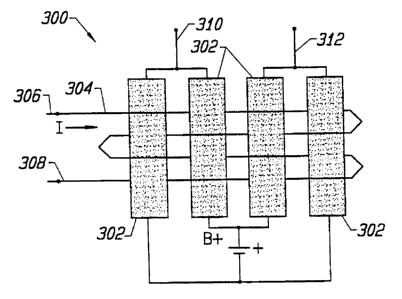
Fig. 3a shows a schematic diagram of a transpinnor 300
designed according to a second embodiment of the invention.
Instead of only one GMR film, this embodiment employs four GNIR
films 302 arranged in a bridge configuration with conductor 304
wound through them for supplying a magnetic field thereto. As
with transpinnor 200, the input of the device (between terminals
306 and 308) is completely isolated resistively from the output
(between nodes 310 and 312) even with a DC input current. Also,
the output voltage of transpinnor 300 is determined by the
magnitude of B+ and the current carrying capacity of GMR films
302. As shown in Fig. 3b, transpinnor 300 has four times the
output of transpinnor 200. Transpinnor 300 also has the advantage
that the bridge is balanced to zero offset if all four films are
identical.
Fig. 4 shows a transpinnor 400 with a closed-flux
geometry which is substantially the same schematically as
transpinnor 300. There is insulation (not shown) in the middle of
transpinnor 400 where top GMR films 402 and 404 nearly touch
bottom GMR films 406 and 408. The four GMR films form a
11
CA 02252926 1998-10-24
WO 97/41601 PCT/US97/07425
G~Theatstone bridge in which the resistance of each is variable.
Input conductor 410 supplies the magnetic field and the output
voltage is provided by output conductors 412 and 414. A bias
voltage B+ is applied between nodes 416 and 418.
Fig. 5 shows a transpinnor 500 with an open-flux
configuration which is substantially the same schematically as
transpinnor 300. GMR film elements 502, 504, 506 and 508 form a
Wheatstone bridge arrangement which requires only a single GMR
deposition (i.e. the GMR layers are deposited in a single pump-
1o down, with no patterning required between deposition of layers).
Such a device was fabricated and tested experimentally. Input
conductor 510 was wound as a single layer of magnet wire. The
closed-flux structure of Fig. 4 gives superior performance,
especially for small-size devices, but involves multiple GMR
depositions and patterning.
Fig. 6 illustrates the relationship between input
current and output voltage for the all-metal GMR transpinnor shown
in Fig. 5. The transpinnor was first initialized by saturating
its four GMR film elements along the easy axes (i.e., parallel to
2o the direction of film strips) with a magnet, and then applying
input current until the magnetization direction of the permalloy
layers in two of the elements switch completely (i.e., for maximum
output from a V~lheatstone bridge two resistors must be in the high
resistance state and two in the low resistance state). After
initialization in this manner, the data for the curve of Fig. 6
were taken. The solid curves, both positive and negative, were
taken starting from the initialized state. The dashed curve is
the remagnetization curve in which the applied field is made more
negative (starting from the state of maximum output) in order to
3o reestablish the initial magnetization state.
The solid curve of Fig. 6 shows a flat portion near the
origin, then a rapid climb in output voltage when the input
current reaches a threshold. It will be understood that this flat
portion and threshold are desirable for digital applications, such
as logic or selection matrices. The flat portion of the curve is
largely due to the exchange bias between the permalloy and the
cobalt layers. For linear applications, this portion of the curve
can be removed either by the application of a small external bias,
or by creating a symmetrical spin valve structure in which two
12
CA 02252926 1998-10-24
WO 97/41601 PCT/US97/07425
cobalt layers are magnetized in opposite directions.
Fig. 7 shows an output voltage vs. input current curve
for the GMR transpinnor of Fig. 6 but with a small external bias
(e. g., 1.5 Oe) applied with a magnet in the easy direction (i.e.,
parallel to the film strips). As is evident, the exchange bias
plateau around the origin has been essentially eliminated. As
with Fig. 6, the solid lines begin with the initialized state, and
the dashed line is the remagnetization curve. The finite
hysteresis makes this transpinnor better suited for digital than
1o for linear applications.
The G1~ transpinnors of Fig. 6 has a rather large
hysteresis in the permalloy of 1 Oe. However, permalloy
coercivities of an order of magnitude smaller are found. This is
of interest because the voltage and current gain of the GMR
transpinnor of the present invention are inversely proportional to
the permalloy coercivity, and the power gain is inversely
proportional to the square of the permalloy coercivity. The
permalloy coercivity found in multi-period GMR films is routinely
much lower than single-period GMR films. The reason is that the
2o domain walls form in pairs in the closely spaced films of the
multi-period devices, greatly reducing the magnetostatic energy of
the walls. This is beneficial for linear applications because it
increases the gain of the transpinnor. Unfortunately, a
corresponding reduction in the coercivity of the cobalt layers is
also found. This reduction is undesirable because at some point
the magnetization direction of the cobalt layers begin to switch
at a lower threshold than the magnetization direction of some of
the perrnalloy layers. Obviously, the proper balance between these
two parameters must be found for the particular application.
3o It is desirable for specific embodiments of the GMR
transpinnor of the present invention to have a gain greater than
unity. The low-frequency gain of these GMR transpinnors is a
function of their fundamental parameters. Referring again to Fig.
5, input line 510 of transpinnor 500 is completely isolated from
the output circuit. For the purpose of calculating the gain of
transpinnor 500, let the input current be i, the input voltage be
v, and the resistance of the input line be r. Furthermore, let
the output voltage of transpinnor 500 be V, the resistance of the
output circuit (including the GMR film) be R, and the sense
13
CA 02252926 1998-10-24
WO 97/41601 PCT/US97/07425
current be I. Let us also introduce a variable to express the
ratio of the percentage change in resistance caused by a small
applied magnetic field. Where the shear is unimportant compared
to the coercivity, this quantity, which we call the resistibility,
X, is given by
X = GMR/ (100H~) (1)
where H~ represents the coercivity of the permalloy in the GN~t
film. The voltage gain of the GMR transpinnor of the present
invention is proportional to the resistibility, and the power gain
is proportional to the square of the resistibility.
The input line of the transpinnor produces a field. The
ratio of field to the current by which it is produced is referred
to herein as the coil efficiency, E. Generally speaking, the
value of E increases dramatically as the size of the transistor
decreases. If other parameters (including the resistance of the
input line) stay the same, the voltage amplification is
proportional to E, and the power amplification is proportional to
2o the square of E.
Given the definitions of the various parameters of the
transpinnor, the voltage amplification is given by
Plroltage = ( R/ r ) I E X ( 2 )
and the power amplification is given by
bower ' ( R / r ) I2 E2 XZ
3o From (1) and (3) it becomes evident that the power amplification
of transpinnor 500 is proportional to the square of the sense
current, to the square of the GMR, to the square of the drive line
efficiency, and inversely proportional to the square of the
coercivity of the GMR film.
Some numerical examples of power amplification may be
instructive. According to a first example, the input resistance
is 0.8 Ohms, the resistance of the GMR film elements is 120 Ohms,
the resistibility is 0.011/0e, and the coil efficiency is
20 Oe/amp. If an input current of 500 mA is used, according to
14
CA 02252926 1998-10-24
WO 97/41601 PCT/US97/07425
(3), the power amplification is 1.8. This is not a particularly
good film.
According to a second example, the parameters are the
same as for the first example above, except that the resistibility
is 0.19/0e. Now the power amplification is 541. This is higher
than desirable for a logic tree, but may be reduced to a desirable
value by appropriately decreasing the sense current.
According to a third example, a miniaturized transistor
is configured as shown in Fig. 4, with the width of its features
1o being on the order of one micron. The copper input conductor is
1 micron thick and 3 microns long. The input resistance is
0.05 ohms, the output resistance is 8 ohms, the coil efficiency is
6000 Oe/amp, the resistibility is 0.19/0e, and the sense current
is 1 mA. The power amplification is then 208.
The conclusion is that substantial power amplification
can be achieved with GMR transpinnors of the present invention
using existing GMR film configurations. Additionally,
amplification factors in the hundreds can be obtained regardless
of whether the transistors are large or so small as to be at the
limits of conventional lithography because the power amplification
factor is independent of the size of the device. However,
although the GMR transpinnors of the present invention scale so
their power amplification doesn't degrade when the devices are
miniaturized, the power handling capability of the devices
diminishes, of course, as the device size diminishes. The GMR
transpinnors of the present invention can be designed to give
either high output current and low output voltage, or high output
voltage and low output current. These parameters are determined
by the aspect ratio of the GMR film. If the GMR film is a long
3o narrow conductor, the output is high voltage and low current. If
the GMR film is a short wide conductor, the output is low voltage
and high current. The power amplification is relatively
independent of the aspect ratio.
To get high power amplification, the following should be
done:
(1) Make the input stripline as thick as possible in order
to lower the resistance r. The power amplification depends only
linearly on r, so this is less critical than the other steps.
CA 02252926 1998-10-24
WO 97/41601 PCT/US97I07425
(2) Make the resistibility as high as possible, either by
raising the GMR or by lowering the coercivity of the permalloy.
(3) Make the GMR films as thick as possible to allow higher
sense current without electromigration problems. This means many
periods (e.g., 15 periods has been employed to obtain GMR of 15~).
Although low GMR films with very low coercivity can be used to
1o construct GMR transpinnors with high power amplification, the
resulting device may be inefficient. If overall power consumption
is a consideration, one should use high GMR films. It is
possible, for example, to make GMR films with GMR of more than
22~.
There are a wide range of applications for which the
transpinnor of the present invention represents a significant
advance. For example, such transpinnors may be employed to
implement nonvolatile logic gates, i.e., gates which maintain
their states when power is removed. Additionally, because all-
2o metal films exhibit much greater resistance to damage by radiation
than semiconductors, the transpinnor of the present invention may
be employed to implement intrinsically radiation-hard electronics.
The curve shown in Fig. 7 exhibits hysteresis. Although
this is not harmful (and may indeed be useful) for logic devices,
for linear transpinnor performance, the hysteresis loop needs to
be closed and straightened in a finite operating region;
additionally, films with very low-coercivity should be used. In
general, the shape of the hysteresis loop of thin films depends on
the direction of the applied fields. Different approaches to
3o achieve anhysteretic GMR films for transpinnor operation in the
linear region, based on three methods of eliminating hysteresis
and distortion from GMR films, are described. One approach is the
application of a transverse (i.e., perpendicular to the easy
direction) bias field having a magnitude slightly larger than the
anisotropy field of the low coercivity element; the signal to be
amplified is applied as a varying easy-axis magnetic field. This
bias field can be supplied by an external coil or magnet, by
individually deposited magnets on each amplifier, or by a current
in a stripline. The effect of the bias is to eliminate the
16
CA 02252926 1998-10-24
WO 9?141601 PCT/US97/07425
hysteresis and to greatly increase the longitudinal permeability,
as described in two publications, Longitudinal Permeability in
Thin Permalloy Films, E. J. Torok and R. A. White, Journal of
Applied Physics, 34, No.4, (Part 2) pp. 1064-1066, April 1963, and
Measurement of the Easy-Axis and Hk Probability Density Functions
for Thin Ferromagnetic Films Using the Longitudinal Permeability
Hysteresis Loop, E.J. Torok et al., Journal of Applied Physics,
33, No. 10, pp. 3037-3041, October, 1962. The mathematics in
these publications can be used to show that when a GMR film of
1o resistance R, having one or more low coercivity layers (e. g.
permalloy) with anisotropy field Hk, is biased with a hard axis
field Ht > Hk, and to which a small easy axis field dHL is applied,
the film will have a corresponding resistance change, dR, given by
dR / dHL = ( GMR ) R / ( H,L-Hk ) ( 4 )
where GMR is the maximum resistance change, and HT must be larger
than the maximum Hk of any region of the film. This differential
resistance change can be quite large if the inhomogeneity of the
2o film is small, and the corresponding amplification can be large.
This is a sensitive method of achieving anhysteretic GMR films by
a transverse-biased permeability. It results in an analog signal
with a linear response within a certain range.
In another approach to eliminating the hysteresis, the
permalloy layer in the transpinnor is driven and sensed in the
hard direction. The cobalt layer is deposited so that its easy
axis is parallel to the hard axis of the permalloy. this is
accomplished by saturating the cobalt layer during its deposition
at 90 degrees from the easy axis of the permalloy. This method
3o does not generally require a bias field during operation; the
exchange bias between the high coercivity layers) and the
permalloy layer is normally sufficient to prevent the hard-axis
loop from opening. The sensitivity of the hard-axis-driven film
is not as good as in the approach based on the transverse-biased
permeability, as described above, but the linearity extends over a
broader range and this method is easier to implement in that it
avoids biasing in the hard direction and driving in the easy
direction.
Yet another approach involves a sampling method. A
17
CA 02252926 1998-10-24
WO 97/41601 PCT/US97/07425
pulse is applied to the transpinnor between each data sample. The
pulse is of sufficient amplitude to saturate the permalloy layers
in the transpinnor to an initial state that is the same regardless
of whatever signal was applied in between. The frequency of the
applied pulse should be higher than the highest frequency of
interest in the signal to be amplified. The result of using
narrow pulses to reinitialize the magnetic material before each
data sample is to erase the magnetic history and to eliminate the
hysteresis in the output. The output can be sensed either with
1o sampling techniques or as an analog output with a low-pass filter.
According to a specific embodiment of the invention, the
all-metal GMR transpinnor is employed to implement selection
matrices for a PRAM, the PRAM being described in the above-
referenced copending U.S. patent application. Several advantages
z5 derive from the fact that the transpinnor and the PRAM cell are
both GMR film devices. Because the transpinnors and the PRAM
cells can be fabricated with the same deposition and masking
steps, fewer process steps are required than for
metal/semiconductor hybrid devices which must employ costly
2o additional semiconductor depositions. Additionally, because the
number of process steps is reduced, the device yields will be
higher, providing additional cost savings.
Because both devices are all-metal, the transpinnors may
be interspersed among the memory cells, allowing shorter lines
25 with fewer bits per line. Moreover, like the PRAM cell, the
performance of the all-metal transpinnor improves as its
dimensions decrease. Therefore, the density of an all-metal GMR
PRAM array based on the transpinnors of the present invention,
unlike that of silicon-based devices, is limited only by the state
30 of the art of lithography. Finally, the transpinnors of the
present invention allow for the salvaging of chips with
manufacturing defects because appropriate routing may avoid the
affected areas of the chip. This is because the nonvolatile
nature of the transpinnors means that the defective gates may
35 effectively be ignored. Thus, according to a specific embodiment
of the invention, the incorporation of the all-metal GMR
transpinnor into a GMR PRAM provides a very high-density,
high-speed, nonvolatile memory which is characterized by a
relatively high manufacturing yield.
18
CA 02252926 1998-10-24
WO 97/41601 PCT/US97/07425
It is generally understood that all possible electronic
circuits, analog and digital, can be implemented using active
components, e.g., transistors, in combination with four basic
passive components, i.e., resistors, capacitors, inductors and
transformers. It is also well known that neither inductors nor
transformers are available in semiconductor bipolar technology.
By contrast, the GMR transpinnors of the present invention can be
employed to provide both of these components. In fact, they are
well suited to provide the basis of a variety of analog, digital
lo and mixed general-purpose all-metal circuits, subsystems and
systems. Since capacitance and resistance can be implemented with
the same metal technology as that used for the passive transformer
and the transpinnor, all these components can be combined very
effectively on the same substrate to produce a comprehensive
variety of all-metal circuits. Unlike semiconductor chips, whose
performance suffers below a critical size, the characteristics of
GMR devices improve as the dimensions are decreased.
Biased in the appropriate operating region, GNgt
transpinnors can be used as basic building blocks of logic gates,
2o thereby providing the foundation for GMR-based digital
electronics. While logic elements can be made with combinations
of transpinnors, just as with transistors, there is another
alternative. Various logic operations can be implemented with a
single transpinnor. These transpinnors have more than one input
line. Examples of such transpinnors are shown in Fig. 8 and 10.
Two procedures are useful in implementing logic gates
with a single transpinnor. One involves setting the transpinnor
threshold which is determined by the coercivity of the low
coercivity layers in the GMR film. Various ways of establishing
3o the coercivity of a thin film are known in the art. Thus, the
threshold is set by choosing or adjusting the coercivity of at
least one of the low-coercivity layers in the GMR films of the
transpinnor. The other procedure involves switching the polarity
of the GMR films which is determined by the magnetization
orientation of all the film layers. The polarity of the
transpinnor is thus switched by reversing the direction of
magnetization of all layers of all GMR films in the transpinnor.
Logic operations which can be implemented with a single
transpinnor include the following:
19
CA 02252926 1998-10-24
WO 97/41601 PCT/US97/07425
AND gate: A transpinnor will not switch unless the sum
of fields from the input lines exceeds the switching threshold.
An AND gate is defined as one that yields no output unless all of
its inputs are logical "1"s. If the transpinnor has n input
lines, and the amplitude of each input pulse is (1/n)th of the
threshold, then the transpinnor is an AND gate.
NAND gate: This is the inverse of the AND gate and
gives an output if and only if all inputs are zero. A transpinnor
NAND gate is made similarly as the AND gate, by reversing the
io magnetization of all elements so that the gate will just switch if
all n inputs are logical "0"s and not switch if one or more are a
logical "1".
OR gate: The definition of an OR gate is one that gives
an output if one or both inputs are a "1". This can be made by
setting the threshold of a transpinnor such that a single input is
sufficient to switch the film.
A practical problem is presented by the fact that
different switching thresholds are required for different single
transpinnor logic gates. There are, however, a variety of ways in
2o which these thresholds may be adjusted for different types of
gates on the same substrate. These include manipulation of the
order of deposition because the order strongly influences the
coercivity of both the low and high coercivity films. This method
involves additional deposition steps. Another method of adjusting
the switching threshold for a particular transpinnor is derived
from the fact that the magnetic field from a current carrying
stripline depends on the width of the strip line.
NOR gate: The definition of a NOR gate is one that
gives an output if one or both inputs are a "0". This is merely
3o the inverse of an OR. This can be done by reversing the polarity
of the GMR films as in the above case of a NAND.
NOT gate: A NOT gate is an inverter that changes the
polarity of an input pulse from positive to negative and vice
versa. This is easily done with a transpinnor by reversing the
polarity of the input winding, or by interchanging the power
terminals.
Exclusive OR gate: This is a gate that gives an output
if one and only one of the inputs is a "I". This can be done with
a transpinnor such that one input is sufficient to switch the low-
CA 02252926 1998-10-24
WO 97/41601 PCT/US97/07425
coercivity element, yielding an output, while two or more pulse
inputs yield a field large enough to switch the high-coercivity
element as well, yielding zero output. The gate must be reset
after each use.
For logic and computer applications, transpinnors with
sharp thresholds and square-pulse outputs are desirable. For
analog applications, a linear response is better. Several methods
of achieving linear transpinnor operation were already discussed
above. Transpinnors operating in the linear region can be used to
1o develop a full complement of basic analog circuits, sufficient to
create general-purpose analog circuitry based on GMR films.
A specific example of a transpinnor operating in the
linear region for application to signal amplification illustrates
some of the unique advantages of the dual functionality of the
i5 transpinnor over silicon technology. Differential amplifiers are
typically used to eliminate common-mode signal and common-mode
noise within the frequency range of their operation. As discussed
above, the range of operation of the transpinnor in its
transformer function extends from (and including) do to the high-
2o frequency cutoff limit. The GMR transpinnor can advantageously be
utilized in its transformer function to remove common-mode signal
in the differential-input mode, as well as in its transistor
function to amplify a low signal in the single-ended output mode.
IN low-signal amplification, GMR transpinnors have the additional
25 advantage of eliminating the problem of offset voltage at the
input that is so troublesome in silicon integrated circuits. It
should be noted that a high premium is paid in silicon technology
to achieve low-offset input voltage for integrated differential
amplifiers. That is, low-offset input voltage is achieved in
3o silicon circuits only at the expense of degrading other
parameters. No such price is associated with the use of
transpinnors because of their dual transformer/transistor
properties. Specifically, the input signal is applied to a
differential input having the properties of a transformer primary
35 with an additional advantage of flat low-frequency response
inclusive to dc. The output signal is amplified by an output
having transistor properties. Transpinnors are thus especially
well suited as differential amplifiers.
Specific embodiments of the invention will now be
21
CA 02252926 1998-10-24
WO 97/41601 PCT/US97/07425
discussed which may be employed to implement various portions of
the selection electronics for an all-metal PRAM. As discussed
above, because one can fabricate the transpinnors described herein
entirely out of GMR films and metal conductors, such transpinnors
can be used to implement the selection electronics (i.e., word and
digit drivers, selection matrices, low-level sense gates,
differential sense amplifiers, etc.) on a GMR PRAM chip.
Conventional silicon-based devices need not be used at all.
According to a specific embodiment of the invention, an
1o array of all-metal transpinnors are employed to implement word and
digit selection matrices for an all-metal GMR PRAM. Fig. 8 shows
one such all-metal GMR transpinnor 800 and two drive lines. Four
GMR films 802 are tied together in a folded Wheatstone bridge
configuration. Each GMR film 802 is shown as a rectangular strip
with its easy axis oriented in the long direction. Flux closure
is also along the easy axis, but is not shown. The two drive
lines (gates #1 and #2) are deposited conductor strips. The
application of current on gate #2 tends to magnetize all four GMR
films in the same direction. The application of current on
2o gate #1 tends to magnetize adjacent GMR films oppositely. With
the proper pulse combinations one can use half-select pulses to
magnetize the high-coercivity layers positively or negatively in
one direction, or to magnetize alternate strips in alternate
directions.
Using the gate lines it is possible to write a magnetic
configuration into a single transpinnor that is different from the
magnetic configuration in all other transpinnors in the selection
matrix. When a half-select pulse is transmitted down a gate line
that traverses a row of such transpinnors, only the one with the
3o different magnetic configuration will emit a pulse. For example,
if all four films in all the transpinnors of the selection matrix
are written uniformly in the same direction, then a half-select
pulse on the gate #2 line would not generate an output in any of
the devices. However, if one transpinnor in the matrix had its
four films alternately magnetized, that transpinnor would generate
an output.
Fig. 9 shows a portion of a selection matrix 900 for
word lines 902. According to a specific embodiment, transpinnors
904 are arranged in a 100 x 100 matrix and can therefore service
22
CA 02252926 1998-10-24
WO 97/41601 PCT/CTS97107425
10,000 word lines 902. Word lines 902 from each transpinnor 904
drive a corresponding memory cell (not shown). The DC power leads
are also not shown. According to this embodiment, similar
circuitry is employed to implement a selection matrix for 10,000
digit lines (not shown). Thus, the total number of bits in the
memory would be 108 bits, i.e., 100 megabits.
The requirements for a sense-line selection matrix are
more stringent than those for the word and digit line selection
matrices. For the embodiment described above having 10,000 sense
lines, a means of selecting only the signal from the desired line
is needed. This requires that inductive and capacitive noise on
the selected word line be minimized. To accomplish this, dummy
lines and differential amplifiers are employed. The same noise is
transmitted on both the sense line and its corresponding dummy
is line, and is cancelled by the differential amplifier. For best
results this cancellation should be done in the first
amplification stage.
Fig. 10 shows a gated GNP differential amplifier 1000
designed according to one embodiment of the invention for use in a
2o sense-line selection matrix. Once again, four GMR films 1002 are
arranged in a Wheatstone bridge configuration. Two input lines
1004 and 1006 supply a switching field to the permalloy layers in
GMR films 1002. If the signals on lines 1004 and 1006 are
identical, no switching takes place and the output (between nodes
25 1008 and 1010) is zero. Any common mode noise is thus rejected.
Gate lines #1 and #2 facilitate selection of one and only one
differential amplifier in the selection matrix. All four lines
(gate lines #1 and #2 and input lines 1004 and 1006) are
electrically isolated, i.e., there is no electrical connection
3o between them or to GMR films 1002 in gated differential amplifier
1000.
According to another embodiment, the read current is
gated by a read-current selection matrix (similar to the word and
digit selection matrices above). In this embodiment, the two gate
35 lines are not required because signals come only from the selected
sense line and dummy line. However, the gate lines may be used to
reset the permalloy after a read operation and, in the case of low
film output, to bias the permalloy to the point of maximum
sensitivity.
23
CA 02252926 1998-10-24
WO 97/41601 PCT/US97/07425
Fig. 11 shows a portion of a sense-line selection matrix
1100 for a GMR PRAM which employs the gated differential amplifier
1000 of Fig. 10. One such differential amplifier is at the end of
each sense line 1102. Nine sense lines 1102 are shown in Fig. 11.
tnThile one could have a dummy line for each sense line, it is not
necessary and is wasteful of space on the substrate. Therefore,
in the embodiment shown, each dummy line 1104 is shared by three
sense lines 1102 as an input to the respective differential
amplifier 1000. It will be understood that the three to one ratio
of sense lines to dummy lines shown in Fig. 11 is merely
illustrative and that higher ratios may be desirable in commercial
products. In an alternative design, active sense lines may also
serve as dummy lines when they are not being interrogated. Gate
lines #1 and #2 for each differential amplifier 1000 are shown
connected to the x lines 1106 and the y lines 1108 of sense-line
selection matrix 1100.
The active GMR transpinnor of the present invention is a
new kind of device having the main characteristics of a
conventional transformer, including: (I) no electrically
2o conductive path between primary and secondary; (ii) signal
transmission from the primary to the secondary via a magnetic
field; (iii) single-ended (unbalanced) and balanced
configurations, each with either inverting or noninverting
polarity; and (iv) the output can be gated. The following
additional properties of the GMR transformer described herein have
no counterparts in a conventional transformer: (v) flat frequency
response down to dc; (vi) current, voltage and/or power gain;
(vii) any integral or nonintegral (i.e., continuous) ratios of
voltage or current between the primary and secondary, as
3o determined by the parameters of the active device.
One embodiment of an active GMR transformer 1200
consists of four GMR films 1202(a)-(d) arranged in a Wheatstone
bridge configuration as shown in Fig. 12. The Vdheatstone bridge
is folded in order to cancel the demagnetizing field and to use
nonmagnetic input line 1204 more efficiently.
At the time of manufacture, transpinnor 1200 is
saturated with a large external magnetic field to the left (with
respect to Fig. 12). A current from left to right in u-shaped
center conductor 1204 causes the permalloy (i.e., low coercivity)
24
CA 02252926 1998-10-24
WO 97/41601 PCT/US97/07425
layer in the GMR film 1202(a) to be magnetized opposite to that of
that film's cobalt layer, and likewise for GMR film 1202(d), thus
increasing the resistance in those two legs of the bridge. This
causes an imbalance in the bridge, resulting in an output voltage
between nodes 1206 and 1208. Reversing the current in the u-
shaped conductor 1204 causes the bridge to be unbalanced in the
other direction, thereby reversing the sign of the output.
It will be understood that GMR transpinnor 1200 can step
up (and step down) the voltage in a manner similar to a
1o conventional transformer. However, unlike a conventional
transformer, the GMR transpinnor is an active device which can
actually have power gain.
There are many applications for transformers, some of
which require that the transformers be gated. For example, many
i5 of the early military thin-film memories used gated transformers
as word and digit gates for selection matrices. An embodiment of
a gated GMR transpinnor 1300 is shown in Fig. 13. Conventional
gated transformers differ from GMR transpinnor 1300 in that the
latter has flat frequency response down to do and can have gain in
2o voltage, current and power.
Instead of a single nonmagnetic conductor for the
introduction of an input signal (as described with respect to
transpinnor 1200), transpinnor 1300 has two such nonmagnetic
conductors 1302 and 1304. Conductor 1304 serves as the gate line
25 and is used to saturate the permalloy components of the GMR films
(1306(a)-(d)) so that no signal is transmitted between primary
conductor 1302 and secondary output nodes 1308 and 1310. Note
that gate conductor 1304 is isolated from primary conductor 1302
and can also be used as an input line. Thus, the device can also
3o be used as a linear mixer, generating a linear sum of two signals
introduced on conductors 1302 and 1304 without distortion. An
example of a typical application of a linear mixer is in a PA
system, where various microphone signals are mixed and fed into an
amplifier. The GMR transpinnor may also be used as a nonlinear
35 mixer, performing logic functions, and/or creating harmonics and
the sum and difference frequencies of two input signals.
In some cases it may be important to increase the
sensitivity of a GMR transformer (defined as the effective
primary/secondary transformation ratio) through the use of a
CA 02252926 1998-10-24
WO 97/41601 PCT/US97/07425
multi-turn input line as shown in Fig. 14. Whereas in a
conventional transformer voltage step-up is obtained by increasing
the ratio of secondary-to-primary turns, in a GMR transformer
designed according to the present invention, the effective voltage
step-up is achieved by increasing the number of turns in the
primary. The secondary remains in the form of a Wheatstone
bridge. Fig. 14 shows a GMR transpinnor 1400 which has such a
multi-turn input conductor 1402 replacing the single-turn
conductor 410 of Fig. 4.
1o According to this embodiment, input conductor 1402 has
four turns, thereby making transformer 1400 four times more
sensitive than a similar design with only one turn (i.e.,
transformer 1600). Shown also is an additional conductor 1404
which is necessary to bring the inside lead of the input coil to
z5 the outside of the device. It turns out that this fabrication
layer is necessary even in single-turn, ungated designs in order
to make the pads thick enough for wire bonding. In actual
practice, this thick layer may be deposited over various segments
of conductors in order to lower the resistance of those segments.
2o Of course, this is feasible only for segments not required to be
thin for the proper operation of the GMR transformer. It will be
understood that the multi-turn design requires more area on the
chip than the single-turn design.
25 At~t~lications
The GMR transpinnor of the present invention is a very
powerful and versatile tool with attractive properties for a
variety of applications. Because there are no inductors or
transformers, either passive or active, in conventional
3o semiconductor technology, the realization of such devices using
GMR technology enables previously unavailable capabilities. The
following are examples of some specific applications for micron
and submicron-scale circuit components.
A linear region of operation enables use of the
35 transpinnor for sensor, amplifier and differential-amplifier
applications, as well as other analog functions. A variety of
logic circuits using active pulse transformers can be developed
for wide and diverse applications, including computer functions
such as a selection matrix for word or digit lines, logic trees,
26
CA 02252926 1998-10-24
WO 97/41601 PCT/US97/07425
adders, ALUs and CPUs, i.e., a radiation-hard all-metal
microprocessor. Combined with the GMR memory and the analog
circuitry, this would open the door to an all-metal computer.
As discussed above with reference to U.S. Patent No.
5,587,943, a GMR-based memory may be constructed which can perform
as reliably as the old magnetic core memories and eliminate the
problems associated with therewith in that such a memory has
nondestructive read, is easy to fabricate, and has an output which
does not shrink as the feature size decreases. This GMR memory
1o also has a decisive advantage over the dominant semiconductor
memory, DRAM, in that it is nonvolatile, i.e., data are retained
after power is removed from the device. The fabrication methods
used for such memories are similar to those used in IC
manufacture. Therefore, the GMR transpinnor of the present
invention, being based on the same underlying technology as this
GMR memory (i.e., multilayer magnetic thin films), provides the
ideal foundation for the support circuitry for such a memory in
that it can be laid down simultaneously by the same process as the
memory array itself.
2o In general, the six-terminal devices described herein
have many more possible uses than conventional three-terminal Si
transistors. The greater number of terminals can be utilized to
implement a wider variety of interesting circuit configurations,
limited only be the creativity of the designer.
Micromechanical systems in general require micron and
submicron-scale electronic systems for their operation, e.g., for
control and interface to intelligent systems. Together, these
form microelectromechanical systems (MEMS), a rapidly growing
discipline. The general GMR circuits described herein can play an
3o integral role in all MEMS applications. Transpinnors and GMR
circuits in general are ideally suited to operate MEMS devices.
For example, many future MEMS will have large numbers of sensors.
GMR circuits can amplify small signals from sensors and process
them for digital compatibility for further processing of data.
In addition, GMR electronics should function well under
the types of environmental stresses that are often encountered in
conjunction with MEMS devices, such as radiation, wide temperature
range, and humidity which necessitates hermeticity requirements.
Finally, being all metal, GMR devices lend themselves to
27
CA 02252926 1998-10-24
WO 97/41601 PCT/US97/07425
fabrication techniques which are likely compatible with
fabrication of some electromechanical devices of micron dimensions
and below.
While the invention has been particularly shown and
described with reference to specific embodiments thereof, it will
be understood by those skilled in the art that the foregoing and
other changes in the form and details may be made therein without
departing from the spirit or scope of the invention. The scope of
the invention should therefore be determined with reference to the
1o appended claims.
28