Note: Descriptions are shown in the official language in which they were submitted.
CA 02253045 1998-11-06
542P19CA
METHOD AND APPARATUS FOR CLEANING HARMFUL GAS
BY IRRADIATION WITH GAS LASER AND ELECTRON BEAMS
BACKGROUND OF THE INVENTION
1. Field of the Invention
The present invention relates to a method and apparatus for
cleaning waste gas generated from power generating machines,
industrial facilities, incinerators, etc., and more particularly
to a method and apparatus for reducing harmful ingredients
l0 contained in the waste gas by dissociating the ingredients by
irradiation with gas laser and electron beams thereto.
2. Description of the Prior Art
Korean Patent Application Laid-Open No. 96-21112 discloses a
conventional method and apparatus for treating waste gas by
irradiation with electron beams. According to this method and
apparatus, ammonia is added to the waste gas mainly containing
sulfuric oxide (SOx) or nitrogen oxide (NOx) , and then the sulfuric
oxide and nitrogen oxide are changed to ammonium sulfate and
ammonium nitrate by irradiation of electron beams thereto, so that
the harmful ingredients, i.e., SOx and NOx, are eliminated from the
exhaust gas. In such a method using ammonia gas for eliminating
the harmful ingredients, however, the ammonia gas is apt to be
exhausted together with the exhaust gas under an incomplete
reaction of the above-described ingredients. Further, this method
and apparatus has problems of necessitating a separate apparatus
for mixing ammonia with the waste gas as well as uneven irradiation
of electron beams into the waste gas.
U. S . Patent No. 4, 915, 916 discloses a method and apparatus for
treating waste gas by irradiation with electron beams without using
1
CA 02253045 1998-11-06
ammonia. According to this method and apparatus, a part of the
waste gas to be treated is irradiated with electron beams to form
active species such as [O] and OH radicals, and the waste gas
having the active species is dispersed into and mixed into the
remaining waste gas to change NOx and SOx in the waste gas into the
form of a mist or dust by the action of the active species. The
mist or dust is then captured by a dust collector. However, this
method and apparatus has problems such as a low efficiency of
eliminating the harmful ingredients and a large size of the
apparatus since the electron beam irradiation region is separated
from the reaction region.
The conventional apparatuses and methods for treating harmful
gas with electron beams as described above also have drawbacks such
that the electron beam irradiation region does not cover the entire
path of the waste gas, and a low density of electron beams results
in a low speed and efficiency of eliminating the harmful
ingredients.
SUMMARY OF THE INVENTION
An object of the present invention is to provide a method and
apparatus for cleaning harmful gas which has a compact size and
high efficiency by defining one region for both a gas laser and
electron beam irradiation region, and an exhaust gas reaction
region, and without the necessity of a separate intermediate
material such as ammonium.
Another obj ect of the present invention is to provide a method
and apparatus for cleaning harmful gas of a high treatment
efficiency and speed by irradiating high-density gas laser and
electron beams throughout the path of the harmful gas.
Still another object of the present invention is to provide
2
CA 02253045 1998-11-06
a method and apparatus for generating a high-frequency and high
voltage signal which can produce gas laser and electron beams
conforming to the above objects.
In one aspect of the present invention, there is provided an
apparatus for reducing harmful ingredients in gas by irradiating
the gas with an electron beam, the apparatus comprising a voltage
generating unit adapted to generate a high-frequency and high
voltage signal, and a reaction unit coupled to the voltage
generating unit to receive the high-frequency and high voltage
signal, the reaction unit including an electron beam pole having
a plurality of openings along the surface of the electron beam
pole, and a plurality of discharge cells for each opening, the
discharge cells being disposed to face the corresponding opening
for generation of the electron beam therebetween, the region
between the discharge cells and the openings defining a reaction
region through which the gas travels.
In a preferred embodiment of the present invention, the
electron beam pole has an annular shape and the openings are formed
around the annular wall of the electron beam pole, and the
discharge cells are stacked and each cell has an electrode tip
pointing toward the corresponding opening.
In the preferred embodiment of the present invention, the
electron beam pole has an annular shape, and the openings are
elongated and disposed at a predetermined angle with respect to the
radial axis of the electron beam pole, and the discharge cells are
stacked and aligned along the corresponding elongated opening, and
each cell has an electrode tip pointing toward the corresponding
elongated opening.
Preferably, each discharge cell of the stacked discharge cells
3
CA 02253045 1998-11-06
for each opening is radially offset from the adjacent discharge
cell by a predefined angle in the range of 5° to 20°.
According to the preferred embodiment, an energy power supply
unit coupled to the voltage generator and the reaction unit to
supply the high-frequency and high voltage signal to the electron
beam pole, the energy power supply unit including a central frame
secured to the electron beam pole, a case secured to the plurality
of discharge cells and surrounding the central frame, and a
coupling member coupling the central frame to the case. The
coupling member comprises a central shaft secured to the electron
beam pole, a pair of reinforcing shafts transversely secured to
both ends of the central shaft, a plurality of insulator terminals
attached to both ends of the reinforcing shafts and having outer
surfaces secured to the case, and an energy input terminal,
attached to an external surface of the case in an insulated state
and connected to the central shaft in a conductive state, for
supplying the high-frequency and high voltage signal from the
voltage generation unit to the electron beam pole.
Preferably, the apparatus for cleaning harmful gas according
to the present invention may further comprise a compressed air
supply unit for supplying compressed air to the reaction region.
In another aspect of the present invention, there is provided
a harmful gas cleaning method for reducing harmful ingredients in
waste gas by irradiation with an electron beam, the method
comprising the steps of converting an AC supply voltage to a high
DC voltage, an oscillating high-frequency high voltage signal, and
a high-frequency high voltage ring waveform signal, combining the
high DC voltage, the oscillating high-frequency high voltage
signal, and the high-frequency high voltage ring waveform signal
4
CA 02253045 1998-11-06
to produce a final signal of high-frequency and high voltage,
generating an electron beam by applying the final signal across a
beam pole and discharge cells, and irradiating the electron beam
against the waste gas passing through a reaction region defined by
the area between the beam pole and the discharge cells.
BRIEF DESCRIPTION OF THE DRAWINGS
The above objects, other features and advantages of the
present invention will become more apparent by describing the
preferred embodiments thereof with reference to the accompanying
drawings, in which:
FIG. 1 is a perspective view illustrating an external
configuration of the harmful gas cleaning apparatus according to
an embodiment of the present invention.
FIG. 2 is a perspective view illustrating a part of the
reaction unit according to an embodiment of the present invention.
FIG. 3 is a perspective view of the electron beam discharge
cell according to an embodiment of the present invention.
FIG. 4a is a top plan view illustrating the electron beam
discharge cells in a laminated or stacked state according to an
embodiment of the present invention.
FIG. 4b is a side view of FIG. 4a.
FIG. 5 is a perspective view illustrating the electron beam
pole according to an embodiment of the present invention.
FIG. 6 is a circuit diagram of the high-frequency and high
voltage generation unit according to an embodiment of the present
invention.
FIGs. 7a and 7b are waveform diagrams of the high-frequency
and high voltage ultimately outputted from the high-frequency and
high voltage generation unit according to an embodiment of the
5
CA 02253045 1998-11-06
present invention.
FIG. 8 is a waveform diagram of the first high DC voltage
generated from the high-frequency and high voltage generation unit
according to an embodiment of the present invention.
FIG. 9 is a waveform diagram of the second high-frequency and
high voltage generated from the high-frequency and high voltage
generation unit according to an embodiment of the present
invention.
FIG. 10 is a waveform diagram of the third high-frequency and
high voltage generated from the high-frequency and high voltage
generation unit according to an embodiment of the present
invention.
FIG. 11 is a waveform diagram of the high-frequency and high
voltage outputted from the high-frequency and high voltage
generation unit according to another embodiment of the present
invention.
FIGs. 12a and 12b are waveform diagrams of the high-frequency
and high voltage outputted from a conventional high-frequency and
high voltage generation unit.
FIG. 13 is a perspective view of the energy power supply unit
according to an embodiment of the present invention.
FIG. 14 is a perspective view of the energy power supply unit
with a part of its case cut-off according to an embodiment of the
present invention.
FIG. 15 is a perspective view of the energy supply terminal
according to an embodiment of the present i-nvention.
FIG. 16 is a perspective view of the electrodes of the
electron beam discharge cells and the reaction hole of the electron
beam pole in an operation state according to the present invention.
6
CA 02253045 1998-11-06
FIG. 17 is a partially sectional view illustrating a plurality
of laminated reaction units secured to the upper and lower end
portions of the energy power supply unit according to the present
invention.
FIG. 18 is an equivalent circuit diagram of the electron beam
discharge cells according to the present invention.
FIG. 19 is a perspective view of an incinerator incorporating
the harmful gas cleaning apparatus according to the present
invention.
DETAILED DESCRIPTION OF THE PREFERRED EMBODIMENT
The harmful gas cleaning apparatus according to the preferred
embodiment of the present invention will be explained with
reference to the accompanying drawings.
The harmful gas cleaning apparatus according to the present
invention includes a high-frequency and high voltage generating
unit (See FIG. 6) for generating a continuous high-frequency and
high voltage signal, which is required for generating gas laser and
electron beams, using commercial AC power, a reaction unit (See
FIGs. 1 to 5) for generating and irradiating the gas laser and
electron beams to harmful gas to cause a chemical reaction on the
harmful gas, and an energy power supply unit (See FIGS. 13 to 15)
for supplying energy from the high-frequency and high voltage
generating unit to the reaction unit and for structurally
supporting the reaction unit.
Now, the construction of the reaction unit of the harmful gas
cleaning apparatus according to the present invention will be
explained with reference to FIGS. 1 to 5.
FIG. 1 is a perspective view of a reactor 10 according to the
present invention. Referring to FIG. 1, the reactor 10 includes
7
CA 02253045 1998-11-06
an energy power supply unit 200, and three reaction units l00
secured to both upper and lower portions of the energy power supply
unit 200. It is also possible that the reactor 10 includes the
energy power supply unit 200, and at least one reaction unit 100
secured to either of the upper and lower portions of the energy
power supply unit 200.
FIG. 2 shows the internal construction of a reaction unit 100
of FIG. 1. Referring to FIG. 2, the reaction unit 100 comprises
an electron beam discharge cell assembly in which a plurality of
electron beam discharge cells 110 are laminated, and an electron
beam pole 120 disposed in an internal space of the electron beam
discharge cell assembly.
FIG. 3 is a perspective view of an electron beam discharge
cell according to the present invention. Referring to FIG. 3, the
electron beam discharge cell 110 is of a perforated plate having
an outer circular periphery 113 and an inner periphery which is
provided with a plurality of triangular electrodes or tips 111
successively formed along the inner periphery. The electron beam
discharge cell 110 also has fastening holes 115, formed spaced
apart from the outer periphery 113, for fastening the laminated
electron beam discharge cells with a fastening member such as a
bolt.
The laminated structure of the electron beam discharge cells
according to the present invention are illustrated in FIGS. 4a and
4b. Referring to FIG. 4a, the electron beam discharge cell
assembly 110 includes a plurality of staggered electron beam
discharge cells laminated in such a manner that an electrode 111
of an upper electron beam discharge cell is offset from a
corresponding electrode of a lower electron beam discharge cell at
8
CA 02253045 1998-11-06
a predetermined angle or distance in a circumferential direction
of the discharge cell, so that, as shown in FIG. 4a, the upper
electrode and the lower electrode partially overlap each other.
The electron beam discharge cell assembly also includes a spacer
150 for separating the laminated electron beam discharge cells from
one another. When the electron beam discharge cells 110 are
assembled with the spacer 115, the fastening holes 115 of the
discharge cells 110 are aligned to mate with those of the spacer
plate 150 to be fastened together.
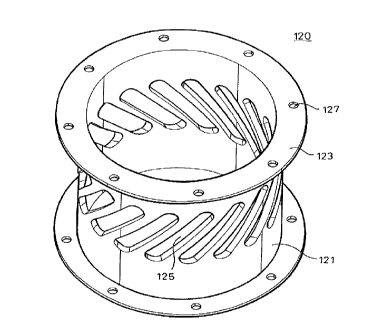
FIG. 5 illustrates the electron beam pole 120 in the reaction
unit 100 according to the present invention. Referring to FIG. 5,
flanges 123 are formed on top and bottom portions of a cylindrical
wall 121 of the electron beam pole 120, and fastening holes 127 are
formed on each flange 123 to fasten a plurality of electron beam
poles 120 together. Reaction openings or slits 125 are formed on
the cylindrical wall 121 of the electron beam pole 120 to face the
electrodes of the electron beam discharge cells 110. The reaction
openings 125 are preferably longitudinally elongated and twisted
at a predetermined angle to correspondingly face the electrodes of
the laminated electron beam discharge cells which are in a spiral
form. As is described later in detail, the angle of the reaction
openings 125 is preferably determined to be in the range of
10°~15°
since it is advantageous in forming high-density gas laser and
electron beams. The number of the laminated electron beam
discharge cells, the number of electrodes of the respective
electron beam discharge cell, and the angle between the electrodes
of the adjacent electron beam discharge cells can be determined to
conform to the angle of the reaction openings 125.
FIG. 6 is a circuit diagram of the high-frequency and high
9
CA 02253045 1998-11-06
voltage generation unit 300 for generating a high-frequency and
high voltage signal suitable for the method and apparatus according
to the present invention and which is applied across the electron
beam poles 120 and the electron beam discharge cells 110. FIGS.
7a and 7b are waveform diagrams illustrating the high-frequency and
high voltage output OUT of the high-frequency and high voltage
generation unit of FIG. 6. The high-frequency and high voltage
output OUT is produced by adding together first to third output
waveforms OUTl, OUT2, and OUT3 as shown in FIGS. 8 to 10 according
to the present invention.
Referring to FIG. 6, the high-frequency and high voltage
generation unit 300 includes three input sections connected to a
primary side of a transformer T. The first input section 310
receives a first commercial AC input voltage VIN1, and includes a
capacitor C1, a resistor RF1, and a coil L1, which serve as an
oscillation circuit. This oscillation circuit also suppresses
noise, and enables a stable output to be obtained from a coil L4
connected to a secondary side of the transformer T.
The second input section 320 receives a second commercial AC
input voltage VIN2, and includes a trigger diode T1 such. as a Zener
diode type, a capacitor C2, and a coil L2, which serve as an
oscillation circuit. The trigger diode T1 is a kind of
bidirectional trigger diode which controls an oscillation cycle by
passing therethrough only the input voltage VIN2 higher than a
predetermined level, so that the second output voltage OUT2 has a
periodic spike-type waveform as shown in FIG. 9.
Preferably, Mylar capacitors, for instance, having a withstand
voltage of 2.5 to 3 times the input voltage may be employed as the
capacitors Cl and C2 in the first and second input sections to
CA 02253045 1998-11-06
obtain an excellent withstand voltage/capacitance characteristic.
The capacitors C1 and C2 should maintain their capacitance below
1~CF, housed by an insulated case, and molded with epoxy resin. The
resistor RF1, which determines a charging/discharging time constant
with the capacitor C1, may be a variable resistor for matching with
the entire high-frequency and high voltage generation unit.
Preferably, a ceramic resistor having a small range of temperature
variation may be employed as the resistor RFl, and the resistance
value of the resistor RF1 may be determined below 1KS2.
The third input oscillation section 330 receives a third
commercial AC input voltage VIN3, and includes capacitors C4 and C5
coupled to each other and thereby defining a common mode G1 of the
third input voltage VIN3, a switching transistor Q1, a coil L3
connected to a collector of the switching transistor Q1, a resistor
Rc connected between an emitter of the transistor Q1 and ground,
and resistors RF2 and RF3 connected to a base of the transistor Q1
through a capacitor C3. The resistor RF2, which determines a
charging/discharging time constant with the capacitor C3, may be
a variable resistor for mating with the high-frequency and high
voltage generation unit. Preferably, a ceramic resistor having a
small range of temperature variation may be employed as the
resistor RF2, and its resistance value may be determined below 1KS2.
The resistor RF3 determines the amplification factor of the
transistor Q1, the resistor Rc is for protection of the transistor
Q1, and the capacitor is a coupling capacitor.
The transistor Q1 in the third input section 330, which is,
for instance, an NPN-type bipolar transistor, is turned on when a
voltage exceeding the bias voltage of the transistor Q1 is applied
through the resistor RF3 to produce an oscillating signal. It is
11
CA 02253045 1998-11-06
preferable that the transistor Q1 has a temperature characteristic
in the range of -40°C to 80°C, and is provided with a heat sink.
Also, the transistor Ql has the operating temperature and
maintenance temperature characteristics suitable for the
environments where the high-frequency and high voltage generation
unit 300 of FIG. 1 is used. As can be appreciated by persons of
ordinary skill in the art, each time the transistor turns on and
off, it generates an oscillation signal and the signal being
generated at the collector of the transistor Q1 looks similar to
the waveform shown as OUT 3, but lower in amplitude. The
transistor Q1 is a high-speed switching transistor with a low loss .
The neutral point or common node Gl corresponds to the level of
"O"V of the third voltage output waveform as shown in FIG. 10.
Preferably, the capacitors C4 and C5 may be of a ceramic type, and
have a withstand voltage of over 3000V and a capacitance of
1000~2000pF or less.
In the embodiment shown, the input voltages VIN1 t0 ViNS of the
first to third input sections 310, 320, and 330 are preferably
single-phase AC voltages of 100~200V, and may be variably supplied
using a slicer. To prevent the characteristic distortion caused
by the voltage variation and the frequency deviation of the input
voltages, variable capacitors (i.e., varicon) may be used as the
capacitors C1, C2, and C3 to tune to a desired input frequency.
The coils L1, L2, and L3 of the respective input sections
constitute the primary windings of the transformer T, and the coils
L4, L5, and L6 constitute the secondary windings of the transformer
T which are connected to the respective output terminals. Here,
it is to be noted that one terminal of each of the coils L4, L5,
and L6, which constitute the secondary windings of the transformer
12
CA 02253045 1998-11-06
T, should be grounded. The withstand voltage of the coils L1 to
L6 should be sufficiently high to withstand damage from application
of 3000V for 10 minutes. When winding the coils, care should be
taken to ensure that the insulating coatings not be damaged. The
primary winding coils L1, L2, and L3 are widely wound using first-
class insulated coils to prevent their deterioration and aging.
The secondary winding coils L4, L5, and L6 are wound also using the
first-class insulated coils. The diameter of the coil L6 is
smaller than that of the coils L4 and L6 since the coil L6 is
mainly for the purpose of producing a high peak voltage rather than
producing current, and the number of turns of the coil L6 is
preferably 5 times that of the coils L4 and L5 to prevent the
reverse flow of the high output voltages OUTl and OUT2. Also, a
section bobbin may be used to wind the coil thereon, and it is
important that the number of turns for each section of the bobbin
should be 300 or less to guarantee the reliability of the coil.
If the number ofturns exceeds 300 for each section of the bobbin,
the electric potential difference of the coil is greatly increased
due to the leakage loss between layers of the wound coil, causing
the deterioration or damage of the coil. Also, if a strong impulse
is produced in the system, the transformer T may deteriorate or
become damaged due to the impulse or ring-wave noise.
Preferably, the transformer T should be insulated by filling
with thermosetting epoxy resin. If normal-temperature-setting
resin is used instead of the thermosetting epoxy resin, the
magnetic field in the transformer may leak due to a setting agent
contained in the resin. Such a magnetic field leakage does not
affect the operating voltage of the system, but may reduce the
efficiency of cleaning specified harmful ingredients. In order to
13
CA 02253045 1998-11-06
solve the problems of the magnetic field leakage, the transformer
is manufactured in such a manner that about 50~ of the insulating
filler material is thermoset after being filled and the bubbles
therein are removed, and then the remaining 50~ of the filler
material is filled and insulation-molded.
A silicon steel plate or a nickel-chrome steel plate may be
used as the iron core of the transformer T. The iron core is
coated with an insulating varnish by impregnation to prevent rust
and water penetration. It is preferable that the iron core has a
thickness of about 0.8mm, and is made of materials having a good
heat dissipation factor and initial magnetic susceptibility.
Meanwhile, the transformer T has the problems of irregular
current supply if heat is generated in the iron core. To solve the
problems, a heat sink (not illustrated) may be attached to the iron
core, and a cooling water pipe may be installed to be in contact
with the heat sink, so that the iron core is cooled to stabilize
the pulse current from the transformer T. A copper pipe is
advantageous to the stabilization of the pulse current, whereas a
non-magnetization or insulation pipe is disadvantageous to the
thermal conductivity and the stabilization of the pulse current.
To the secondary winding coil L4 is connected a first output
section 340 which includes, for instance, a three-stage smoothing
circuit HDl and HCl, HD2 and HC2, and HD3 and HC3, which comprises
very high voltage rectifying diodes HD1, HD2, and HD3 and
capacitors HC1, HC2, and HC3. The AC voltage induced in the coil
L4 is rectified and smoothed through the smoothing circuit, and
accordingly, a DC voltage as shown in FIG. 8 is outputted as the
first output voltage OUT1. Here, the diodes HD1 to HD3 are high
14
CA 02253045 1998-11-06
voltage rectifying diodes having a withstand voltage characteristic
of about 120 of their output voltage. The capacitors HC1 to HC3
have a withstand voltage of about lOKV or more, and their
capacitance values are determined to be HC1<HC2<HC3. Especially,
it is desirable that the capacitor HC3 is used in the range of
10~15KV, considering the safety of the capacitor HC3.
The output voltage OUT1 of the first output section 340 is a
high rectified DC voltage which has the waveform as shown in FIG.
8, and whose peak value VPp thereof is in the range of 10~12KV.
More-stabilized DC voltage output can be obtained by increasing the
withstand voltage of the capacitor HC3.
To the secondary winding coil L5 is connected a second output
section 350 which includes two smoothing circuits HD4, HD5, HC4,
and HD6, HCS, and a matching coil Lm for impedance matching. The
diodes HD4 to HD6 are high voltage rectifying diodes, and have the
withstand voltage characteristic of about 120 of their output
voltage. The diodes HD4 and HD5 heighten the current flowing
therethrough to prevent the reverse flow of the current . It is
preferable that the capacitors HC4 and HC5 have the same withstand
voltage and the same capacitance value. Otherwise, the leakage
current increases through the capacitors.
The output voltage OUT2 of the second output section 350 forms
a periodic spike wave DC-offset by a predetermined voltage level
as shown in FIG. 9. The secondary current of this spike wave is
determined by the diodes HD4 and HDS. The periodic spikes are due
to the trigger diode Tl.
The output voltage OUT3, which is directly outputted from the
coil L6, forms a ring wave as shown in FIG. 10. The ring wave has
a peak value VP and an oscillating wave following the peak value.
CA 02253045 1998-11-06
In the ring wave, the peak value VP is important, but the
oscillating wave can be ignored. The peak value VP, which in this
embodiment is determined to be in the range of 10~20KV, is an
important parameter of the reaction unit wherein the gas laser is
generated by generating and accelerating the electron beams by the
electrodes. The peak value should be consistent with the
dielectric constant in the reaction unit.
The three output voltages OUT1 to OUT3 as described above are
matched by a resistor Rx and a capacitor Cx to produce a final
output voltage OUT. This final output voltage, which is a high
voltage, high frequency signal, is supplied to the system as the
energy power. The resistor Rx is for preventing the overcharge
between the reaction unit 100 and the high-frequency and high
voltage generation unit 300, and it is desirable that the
resistance value of the resistor Rx be in the range of 500~700MS2.
If the resistance value of the resistor Rx exceeds 700MS2, an
operator and a measuring equipment may be injured and damaged due
to the static electricity phenomenon.
The output voltage OUT of the high-frequency and high voltage
generation unit 300 of FIG. 6 has a waveform as shown in FIGS. 7a
and 7b in different time scales. FIG. 7a illustrate the output
voltage OUT on the time base in the unit of ~.sec(10-6 second), and
FIG. 7b illustrate the output voltage OUT on the time base in the
unit of msec(10-3 second). To compare the output voltage OUT with
the output voltage of the conventional electron beam energy power
supply unit, the conventional output voltage waveform is
illustrated in FIGs. 12a and 12b using the time bases in the unit
of .sec and in the unit of msec, respectively. Upon comparing the
two output voltage waveforms, the conventional output voltage is
16
CA 02253045 1998-11-06
an oscillating waveform which varies from negative voltage to its
peak voltage VP about the OV level, whereas the output voltage OUT
according to the present invention is a periodic spike (pulsed)
wave which is heightened or DC-offset by a DC voltage level VPp as
shown in FIG. 7a.
Meanwhile, as shown in FIG. 11, the output voltage which is
DC-offset by the voltage level VPp may be obtained by adding the
first output voltage OUT1 to the third output voltage OUTS. While
possible, this output voltage is somewhat unstable and weak to
obtain the continuous electron beams, and thus the final output
voltage OUT capable of generating the electron/laser beam is
obtained by adding the second output voltage OUT2 to the DC-offset
voltage of FIG. 11.
As can be appreciated by persons of ordinary skill in the art,
the unit 300 can be very compact and is inexpensive to build.
The final output voltage OUT produced as above by the high-
frequency and high voltage generating unit 300 is supplied to the
reaction unit 200 through the energy power supply unit 200. The
energy power supply unit 200 serves to connect thereto the electron
beam discharge cell assembly and the electron beam pole in the
reaction unit 100. The unit 200 also supplies the high-frequency
and high voltage to the reaction unit 100.
Now, the construction of the energy power supply unit 200 will
be explained with reference to FIGS. 13 to 15.
FIG. 13 is a perspective view of the energy power supply unit
according to the present invention. Referring to FIG. 13, the
energy power supply unit 200 includes a central frame 210 secured
to the electron beam pole 120 of the reaction unit 100, a case 220
secured to the electron beam discharge cell assembly and
17
CA 02253045 1998-11-06
surrounding the central frame 210, and a coupling member 230 for
coupling the central frame 210 to the case 220 in an insulated
state and in electrical contact with the central frame 210 to
supply the high-frequency and high voltage signal from the high-
s frequency and high voltage generation unit 300 to the central frame
210.
FIG. 14 illustrates the structure of the energy power supply
unit with the case partially cut-off. Referring to FIG. 14, the
central frame 210 has a cylindrical wall 211 having the same
diameter as the electron beam pole 120 of the reaction unit 100 and
flanges 213 formed on top and bottom portions of the cylindrical
wall 211. The flange 213 has fastening holes 215 formed thereon
for securing the flange 213 to the flange 127 of the electron beam
pole 120. The case 220 is in the shape of a box whose top and
bottom surfaces are open, and has flanges 223 formed on top and
bottom portions thereof. A cover (not illustrated) is secured to
the flange 223 through fastening holes 225. The cover is secured
to the electron beam discharge cells 110 so that the central frame
210 and the electron beam pole 120 penetrate the cover, enabling
the harmful gas to pass therethrough. Also, on both sides of the
case are formed cylindrical portions 227 extending outward, and on
both sides of the cylindrical portion 227 are formed insulator
terminal mounting portions 229 extending outward.
The coupling member 230 includes a central shaft 231 secured
to the central frame 210 in a conductive state, reinforcing shafts
232 perpendicularly secured to both ends of the central shaft 231,
a plurality of insulators terminal 233 having a center portion
attached to the end of the reinforcing shaft 232 and a
circumferential portion secured to the cylindrical portion 227 of
18
CA 02253045 1998-11-06
the case 220, and an energy input terminal 240, attached to an end
of the cylindrical portion 227 of the case 220 in an insulated
state and connected to the central shaft 231 in a conductive state,
for supply current from the high-frequency and high voltage
generation unit to the electron beam pole 120.
The energy input terminal 240, as shown in FIG. 15, includes
a circular base plate 241 attached to the end of the cylindrical
portion 227 of the case 220, and an insulation pipe 245 for
insulating wires (not illustrated) drawn from the base plate 241
and the high-frequency and high voltage generation unit 300. The
energy input terminal 240 also includes a port 243 for supplying
compressed air to the reaction unit 100. The air supplied from the
port is then provided to the reaction unit 100 through a gap 247
between the base plate 241 and the insulation pipe 245.
The harmful gas cleaning operation effected by the harmful gas
cleaning apparatus as described above will now be explained.
The harmful gas cleaning operation may be divided into three
processes: a first process of generating the high-frequency and
high voltage signal by the high-frequency and high voltage
generating unit, a second process of generating the gas laser and
electron beams by supplying the generated high-frequency and high
voltage to the reaction unit, and a third process of reducing the
harmful ingredients in the waste gas by the generated gas laser and
electron beams.
Referring again to FIG. 6, the single-phase AC voltages of
100~200V, 50~60Hz are inputted to the first to third input sections
310, 320, and 330 as their input signals VINE to VIN3, causing the
first to third input sections 310, 320, and 330 to oscillate,
respectively.
19
CA 02253045 1998-11-06
The oscillated pulses from the first to third input sections
310, 320, and 330 are respectively boosted to high voltages by the
transformer T. The high voltage induced in the secondary winding
coil L14 of the transformer T1 is rectified and smoothed by the
first output section 340, and thus the high DC voltage as shown in
FIG. 8 is outputted from the first output section 340 as the first
output voltage OUTl. The high voltage induced in the secondary
winding coil L5 is processed through the second output section 350
which includes the two smoothing circuits HD4, HDS, HC4, and HD6,
HC5, and the impedance matching coil Lm, and thus the periodic
spike-wave voltage as shown in FIG. 9 is outputted from the second
output section 350 as the second output voltage OUT2. The ring-
wave voltage as shown in FIG. 10 is directly outputted from the
secondary winding coil L6 as the third output voltage OUT3. The
three output voltages OUT1 to OUTS are matched by the resistor Rx
and the capacitor Cx, and the final output voltage OUT as shown in
FIGS. 7a and 7b is obtained therefrom.
This output voltage OUT of the high-frequency and high voltage
generating unit of FIG. 6 is a high-frequency and high voltage
having a very short period of about lOns and a peak voltage level
of at least 1KV and preferably about 10KV or more as shown in FIGs.
7a and 7b. This high-frequency and high-voltage energy power is
supplied to the electron beam pole 120 of the reaction unit 100 via
the energy power supply unit 200.
Accordingly, an electric field is formed between the electron
beam pole 120 and the electrodes 111 of the electron beam discharge
cells 110, and the electron beams are irradiated from the
electrodes of the electron beam discharge cells 111 to the reaction
openings 125 of the electron beam pole 120. At this time, as shown
CA 02253045 1998-11-06
in FIG. 7a, since the pulses are supplied such that a DC
electrostatic force of about lOKV or more is constantly maintained,
coherence laser beams are simultaneously generated in addition to
the generation of the electron beams. Further, as shown in FIG.
16, the width of the generated beams is extended due to the twisted
configuration of the reaction openings 125 of the electron beam
pole 120, which conforms to the laminated configuration of the
electrodes of the electron beams discharge cells 110, and this
causes new coherence laser beams to be extended and irradiated from
the incident wave.
FIG. 18 schematically illustrates an equivalent circuit of the
reaction unit of FIG. 2. Referring to FIG. 11, since in the
reaction unit, an electrode 111 of the electron beams discharge
cell and the electron beam pole are considered to constitute a
capacitor, the reaction unit may represent the equivalent circuit
of FIG. 18. Specifically, the reaction unit is composed of a
plurality of capacitors connected in parallel to one another, and
thus a large amount of noise is produced during the operation of
the reaction unit . Such noise is discharged outside, following the
flow of the exhaust gas. However, as shown in FIG. 1, since the
reaction units 100 are connected to connectors 140 and an exhaust
pathway 130, the entire apparatus serves as a sound absorber for
reducing the noise while the exhaust gas repeatedly expands and
contracts, passing through the reaction units 100, connectors 140,
and exhaust pathway 130.
Referring to FIG. 4a, upon looking down the reaction unit from
the top, it can be imagined that a plurality of electron beams are
discharged from the respective electrodes to the reaction openings,
and thus the gas laser and electron beams are irradiated to the
21
CA 02253045 1998-11-06
reaction region between the electrodes and the electron beam pole
in the form of a network of several thousands of meshes. On the
center portion of the reaction region, white wave effect appears,
a strong ionic wind blows, and a strong diffracted wind blows in
a counter-clockwise direction in FIG. 4a.
When the waste gas containing harmful ingredients such as NOx,
SOx, HC, etc., flows into the reaction region formed as above, the
harmful ingredients are dissociated by the high-density electron
beams, and thus the harmful ingredients are eliminated through the
oxidation/reduction reaction of the harmful ingredients.
For example, it was confirmed that in case of an inflow of NOx
to the reaction region, N2 and 02 were produced by the radiated
electron beams by an experiment. Meanwhile, another experiment was
carried out in the cleaning ability of the apparatus with respect
to the exhaust gas from a diesel engine, which contains a high
amount of NOx and HC. In this experiment, it was recognized that
the oxidation radicals related to the elimination of NOx were
mainly O, HO2, and OH, while ozone(03) contributed to the oxidation
of NOx in addition. In detail, 03 contributed to the elimination
of NOx by a harmful ingredient produced with the [O] radical by
dissociation of OZ in the reaction unit. Most of the resultant
harmless ingredient was not discharged to the air, but was adsorbed
by the carbon composition which was thinly deposited on the
electron beam discharge cells 111 and the electron beam pole.
Also, SOx was dissociated by the dissociation reaction of
SOx-~S+x [O] and then eliminated.
The atomic nitrogen (N) produced by dissociation of N2 also
contributed to the elimination of NOx by the reaction of
N+NOx->NZ+x0 .
22
CA 02253045 1998-11-06
However, it was recognized that since N reacted with OH, H02,
and OZ to produce NO, it was advantageous to flow compressed air
into the reaction region for the effective elimination of NOx.
Specifically, by theinflow of the compressed air in addition to
the waste gas, the water contained in the compressed air was
dissociated (HZO->H2+2 [O] ) to expedite the reaction. The compressed
air flowed into the reaction unit 100 through the compressed air
input port 243 of the energy input terminal 240 as shown in FIG.
15.
It is preferable that the harmful gas cleaning apparatus
according to the present invention include a high-frequency and
high voltage generating unit, an energy power supply unit, and a
plurality of reaction units which are secured to the top and bottom
portions of the energy power supply unit in turn. FIG. 17
illustrates such an apparatus in which the energy power supply unit
200 is positioned on the center, and three reaction units 100 are
secured on both the top and bottom portions of the energy power
supply unit 200.
Referring to FIG. 17, the waste gas is indrawn from "A"
position and exhausted to "B" position. The waste gas passes
through the reaction regions each of which is formed between the
electron beam discharge cells 110 and the electron beam pole 120
for irradiating the electron beams, and thus the harmful
ingredients in the waste gas are eliminated. At this time, though
the flow of the waste gas from "A" position to "B" position is very
fast, substantially all of the waste gas is reacted by the electron
beam when passing through the apparatus. That is because the
density of the gas laser and the electron beams in the reaction
units is very high, and the reaction units 100 are in the form of
23
CA 02253045 1998-11-06
a circle, resulting in that the gas laser and electron beams are
irradiated over the whole region of the exhaust gas pathway. Also,
since the gas laser and the electron beams are irradiated with a
very short wavelength, the harmful ingredients in the waste gas are
inevitably exposed to the gas laser and the electron beams to be
reacted though the waste gas passes through the reaction regions
at a high speed.
The harmful gas cleaning apparatus according to the present
invention can be mounted on a small exhaust system such as a
vehicle. Also, several apparatuses connected together in parallel
may be mounted on an incinerator to increase the efficiency and
capacity of the harmful gas treatment as shown in FIG. 19.
The present method and apparatus for cleaning harmful gas can
be applied to diverse fields. For example, it can be used for
treating waste gas produced in incinerators, industrial facilities,
various power generating machines, etc. It can also be used as an
air cleaner in living spaces, industrial sites, underground spaces
such as a tunnel, etc. since it also serves as an air cleaner and
deodorizer. Further, it can be used as a sterilizer or pasteurizer
by its ozone generating function, while it can be employed in
medical appliances, oxygen generating apparatus, food sanitation
facilities, etc. Furthermore, it will be obvious to any person of
ordinary skill in the art that the present apparatus can be applied
to diverse fields such as purifiers for centralized heating/cooling
facilities, waste water disposal plants, waste disposal plants for
reclamation, VOC treating apparatuses, artificial raining
facilities, diverse apparatuses for kitchen works, etc.
An experiment for estimating the harmful gas reducing
performance of the method and apparatus according to the present
24
CA 02253045 1998-11-06
invention was made and the results are shown in Table 1 below. In
the experiment, the power of AC 100V, 400mA was supplied to the
energy power generation unit 200 of the harmful gas cleaning
apparatus.
Table 1
Inflow Exhaust Reduction
Analysis item
Concentration Concentration Rate
Smoke 20~ 3~ 85
CO 5000ppm 1500ppm 70
HC 5000ppm 71500ppm 70
NOx 3000ppm 1200ppm 60
SOx 3000ppm 1200ppm 60
PM (Particle
0.5mg/m2 0.15mg/mz 70
Materials)
Also, it was indirectly confirmed by a biological test whether
an unconfirmed material such as dioxine, which is very harmful to
the living things and contained in the waste gas, and whose
chemical composition or structure has not yet been confirmed
accurately, was dissociated or reduced in the harmful gas cleaning
apparatus according to the present invention.
First, the gas generated by combustion of garbage and waste
tires was gathered and dissolved in distilled water to obtain its
concentrated solution. This concentrated solution of 100cc was
poured into a fish bowl which had the capacity of 10 liters and
contained fish, and all the fish died within several minutes.
Meanwhile, the gas generated by combustion was also treated through
the apparatus of the present invention, and the treated gas was
gathered and dissolved to obtain its concentrated solution. This
CA 02253045 1998-11-06
concentrated solution was poured into a fish bowl, but it was
confirmed that all the fish in the bowl still lived and grew
without death.
According to the direct measurement of the harmful gas
reduction rate, and the indirect biological test as described
above, it has been recognized that the harmful gas cleaning
apparatus according to the present invention has a superior effect
on the reduction of harmful ingredients in the waste gas.
As described above, since the harmful gas cleaning apparatus
according to the present invention generates high-density gas laser
and electron beams in a compact device, it can permit easy
transport and easy installation, and thus can be attached to
vehicles at a low price. Also, its cleaning efficiency can be
easily improved by connecting a plurality of reaction units
together in series. Meanwhile, several apparatuses according to
the present invention may be connected together in parallel so as
to be easily applied to large-capacity exhaust machines or
incinerators.
While the present invention has been described and illustrated
herein with reference to the preferred embodiment thereof, it will
be understood by those skilled in the art that various changes in
form and details may be made therein without departing from the
spirit and scope of the invention.
26