Note: Descriptions are shown in the official language in which they were submitted.
CA 022~332~ 1998-11-10
~13~23 - ~
Specification
Title of the Invention
Microwave Testing High-Power Dummy Load
Forming Method and Microwave Testing
5High-Power Dummy Load Apparatus
Background of the Invention
The present invention relates a microwave
testing dummy load forming method and a microwave
testing dummy load apparatus.
A conventional dummy load of this type having
a large capacity of 1 kW or more requires a large
resistive element. For this reason, some dummy load is
formed as an oil- or water-cooled dummy load, which is
generally formed such that a metal film is deposited on
the surface of a porcelain member, and the member is
dipped in an insulating oil or water. However, this
dummy load is expensive and hence is not practical.
A dry dummy load, which can be manufactured at
a low cost and demands no maintenance, has a structure
in which microwave power is input from an input external
conductor 5 to a resistive element 14e on a dielectric
substrate 11, as shown in Figs. 4A and 4B. The
resistive element 14e is formed by depositing a metal
film such as a carbonyl iron powder or graphite film on
the surface of an insulator with a low thermal
resistance, e.g., beryllia or alumina. Reference
CA 022~332~ 1998-11-10
numeral 13 denotes a ground conductor.
A dummy load apparatus is disclosed in
Japanese Patent Laid-Open No. 61-147601 (reference 1) as
an apparatus in which input microwave power is
distributed to a plurality of termination resistors to
reduce the load on each termination resistor.
In the dummy load apparatus disclosed in
reference 1, hybrid circuits 15, 16, and 17 are formed
on a dielectric substrate 11, and the hybrid circuits 15
and 16 and the hybrid circuits 15 and 17 are connected
to each other through resistive center conductors 12a
and 12b, respectively, as shown in Figs. 5A and 5B.
Output center conductors 12e and 12f of the hybrid
circuit 16 are connected to termination resistors 14c
and 14d. Output center conductors 12c and 12d of the
hybrid circuit 17 are connected to termination resistors
14a and 14b. The termination resistors 14a to 14d are
connected to a common ground conductor 13.
For example, a dummy load of 3W can therefore
be formed by setting the rated power of each of the
termination load 4a to 4d to
3W x 1/4 = 750 mW
In addition, if the termination resistors are
flat resistors, the allowable power per unit area is a
maximum of 30 mW/mm. The area of one termination
resistor is therefore given by
750 . 30 = 25 mm
CA 022~332~ 1998-11-10
In the former dry dummy load apparatus
described above, a beryllia porcelain member having a
very low thermal resistance is mainly used as a
porcelain member on which a resistive film is formed.
However, a beryllia porcelain member is expensive,
requires a resistive film having a large area in
proportion to the allowable power, and suffers a
deterioration in impedance characteristics because an
increase in area leads to an increase in stray
capacitance. Owing to these problems, as a dummy load
apparatus of this type, an apparatus having a power
capacity of about 500 W at most can be commercially
available at present in consideration of limitations
associated with manufacturing techniques, price, and
temperature rise, and the like. Even if a heat
radiation plate is directly mounted on this porcelain
member, only a dummy load apparatus having a power
capacity of about 1 kW at most can be used in practice.
In the latter dummy load apparatus designed to
distribute power to a plurality of termination resistors,
the center conductors 12 and 12a to 12f are formed as
thin films on the dielectric substrate 11, as shown in
Fig. 5B. Since this structure is formed without any
consideration of a temperature rise, only a power
capacity of several W can be obtained.
Summary of the Invention
It is an object of the present invention to
~ , . . .. . .
CA 022~332~ 1998-11-10
provide a microwave testing high-power dummy load
forming method and a microwave testing high-power dummy
load apparatus, in which the dummy load has impedance
characteristics that allow its use in a broad band.
It is another object of the present invention
to provide a microwave testing high-power dummy load
forming method and a microwave testing high-power dummy
load apparatus, in which the dummy load can have a power
capacity of several kW.
In order to achieve the above objects,
according to the present invention, there is provided a
microwave testing high-power dummy load forming method
comprising the steps of connecting a first center
conductor, to which microwave power is input, to a power
distributor formed from a second center conductor having
an output-side distal end branching into a plurality of
portions, thereby separating the microwave power input
to the first center conductor into a plurality of
outputs in correspondence with the output-side distal
end of the second center conductor, connecting a
plurality of termination resistors between the
output-side distal end of the second center conductor
and a ground conductor to make the termination resistors
consume the microwave power, and radiating heat
generated by the termination resistors upon consumption
of the microwave power.
CA 022~332~ 1998-11-10
Brief Description of the Drawings
Fig. 1 is a perspective view showing a
microwave testing high-power dummy load apparatus
according to an embodiment of the present invention;
Fig. 2A is a cross-sectional view taken along
a line A - A in Fig. 1, and Fig. 2B is a longitudinal
sectional view taken along a line B - B in Fig. 1;
Fig. 3 is a flow chart showing a microwave
testing high-power dummy load forming method according
to the present invention;
Fig. 4A is a plan view of a conventional
microwave testing dummy load, and Fig. 4B is a sectional
view taken along a line C - C in Fig. 4B; and
Fig. 5A is a plan view of another conventional
microwave testing dummy load, and Fig. 5B is a sectional
view taken along a line D - d in Fig. 5A.
Description of the Preferred Embodiment
The present invention will be described in
detail below with reference to the accompanying drawings.
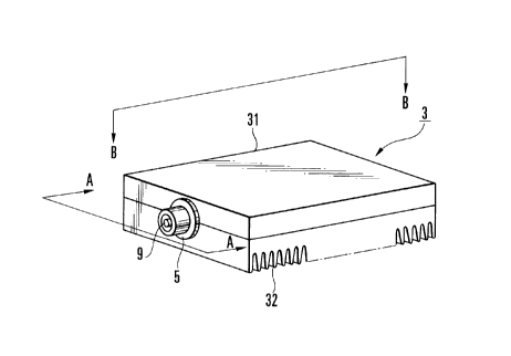
Fig. 1 shows a microwave testing high-power
dummy load apparatus according to an embodiment of the
present invention. The high-power dummy load apparatus
shown in Fig. 1 is used to test TV and FM broadcasting
transmitters.
In the high-power dummy load apparatus in
Fig. 1, a ground conductor upper cover 31 and a ground
conductor radiator 32 are fastened together with screws
.
CA 022~332~ 1998-11-10
to form a ground conductor housing 3 having an internal
space. An input external conductor 5 in the form of a
stepped sleeve is mounted on a side surface of the
ground conductor housing 3.
As shown in Fig. 2A, a cylindrical input
center conductor 9 is placed in the center of the input
center conductor 5. The input center conductor 9 is
connected to an impedance transformer type power
distributor 2 placed in the internal space of the
housing 3. The power distributor 2 is formed from a
flat center conductor 21 having a forked distal end
portion.
As shown in Fig. 2B, the flat center conductor
21 is fixed to the ground conductor housing 3 with
insulators 4. Termination resistors 1 are fixed to the
ground conductor radiator 32 with metal mount plates 6
and screws 10 at positions near the forked distal end
portion of the flat center conductor 21. The
termination resistors 1 are connected to the forked
distal end portion of the flat center conductor 21 of
the power distributor 2 through lead terminals 7.
The input center conductor 9 is fixed to the
center of the input center conductor 5 with an insulator
8. The input center conductor 5 and the input center
conductor 9 serve as a connector for an external
transmission line. Although the insulators 4 and 8 are
made of beryllia, they may be made of a ceramic material
CA 022~332~ 1998-11-10
such as alumina. The ground conductor radiator 32 has a
heat radiation structure with a lower surface having a
comb-like cross-section.
In the high-power dummy load apparatus having
the above structure, microwave power input from the
input center conductor 9 is separated into two outputs
by the power distributor 2, and the respective outputs
are consumed by the two termination resistors 1. Since
the power distributor 2 is formed from the flat center
conductor 21 having a thickness of several mm, the loss
incurred is much smaller than that incurred in a power
distributor formed from a thin metal film. This allows
high-power distribution.
Although power is consumed by the termination
resistors 1, the heat generated by the termination
resistors 1 is conducted to the ground conductor
radiator 32 through the metal mount plates 6 and the
ground conductor upper cover 31 to be radiated. As a
result, a temperature rise caused by the heat generated
by the termination resistors can be suppressed low.
According to the high-power dummy load
apparatus of this embodiment, input microwave power is
separated into a plurality of outputs, and the
respective outputs are consumed by the termination
resistors. In addition, the heat generated upon
consumption of power is radiated through the ground
conductors. Therefore, a microwave testing dummy load
CA 022~332~ 1998-11-10
apparatus with a large power of several kW can be
realized by using existing termination resistors.
Fig. 3 is a flow chart showing a microwave
testing high-power dummy load forming method according
to the present invention. The high-power dummy load
apparatus shown in Fig. 1 is applied to this method.
Referring to Fig. 3, first of all, input
microwave power is separated into a plurality of
microwave powers by the impedance transformer type power
distributor 2 using the flat center conductor 21, and
the respective powers are output (step Sll).
The flat center conductor 21 forming the power
distributor 2 is supported on the ground conductor
housing 3 through a plurality of insulators 4 and 8
(step S12).
The termination resistors 1 are connected
between the ground conductor housing 3 and the forked
distal end portion of the flat center conductor 21 of
the power distributor 2 to consume the microwave powers
(step S13).
Subsequently, the termination resistors 1 are
connected to the ground conductor radiator 32 having the
heat radiation structure to radiate the heat generated
upon consumption of the microwave powers (step S14).
In the microwave testing dummy load formed by
this method, the power consumed by one termination
resistor is reduced. Therefore, the overall capacity of
.. ~ . . ..
CA 022~332~ 1998-11-10
the dummy load increases. In addition, the heat
generated when powers are consumed by the termination
resistors 1 is guided to the radiator 32 of the ground
conductor housing 3 to be effectively radiated. As a
result, a temperature rise caused by each termination
resistor 1 can be suppressed low, and the capacity per
termination resistor 1 can be increased. Therefore, the
overall power consumption capacity of the dummy load
apparatus increases.
As has been described above, according to the
present invention, since the load on each termination
resistor can be reduced by separating input microwave
power into a plurality of powers through the power
distributor, a large-capacity dummy load apparatus can
be realized. In addition, since the power distributor
is formed by using the flat center conductor, a capacity
much larger than that obtained when a center conductor
is made of a thin metal film can be easily obtained.
Furthermore, since an impedance transform type
power distributor is used as the above power distributor,
an increase in capacity can be attained more effectively.
In addition, since the ground conductor serves as a heat
radiation plate, the heat generated by the termination
resistors can be radiated. This suppresses a
temperature rise, leading to an increase in the capacity
of the apparatus.