Note: Descriptions are shown in the official language in which they were submitted.
CA 022~3466 1998-11-03
W O 97/43867 PCTrUS97/09098
METHOD AND APPARATUS FOR PROVIDING MULTIPLE MULTICAST
COMMUNICATION SESSIONS IN AN ATM DESTINATION SWITCH
BACKGROUND OF THE INVENTION
1. Field of the Invention
The present invention relates broadly to
telecommunications. More particularly, the present invention
relates to an ATM destination switch having multicast
capabilities. For purposes herein, the term "destination switch"
is to be understood in its broadest sense to include any call-
terminating switch, access switch, router, or multiplexer located
at the ATM-network/user-line interface.
2. State of the Art
In an ATM network, it is often desirable to effect a
multicast of ATM cells; i.e., to transport ATM cells from a
source terminal to a plurality of different destinations. Each
of the destinations of the multicast will typically have its own
address. Thus, it is necessary to duplicate the ATM cells,
provide different headers for each of the cells, and send the
cells out on different virtual circuits (VCs). In multicast
situations, it is possible that some of the multiple destinations
are connected to a single destination switch (e.g., several
destinations may be coupled to a single local area network
(LAN)). In such situations, it is desirable to reduce the
transport load on the network by sending only a single copy of
each multicast cell to that destination switch element, and to
inform the receiving destination switch element of its
responsibility to send the cell to each of the multiple
destinations which are coupled to it. It has been proposed in
the art that the destination switch element would accomplish the
multicasting of the cell to the multiple destinations in the
standard manner of providing the received cell with unique VCIs
for each of the multiple destinations.
The advantages of transporting a single cell across a
network and then multicasting the cell to a plurality of
CA 022~3466 1998-11-03
W O 97/438G7 PCT~US97/09098
destinations coupled to a destination switch element are that the
network bandwidth usage is reduced, and the cell delay variation
is likewise reduced. On the other hand, if the destination
switch element must multicast an incoming cell to multiple
destinations, the switch element must conduct several VC address
translations. As will be appreciated by those skilled in the
art, a VC address translation requires either a large amount of
logic and memory to enable a hashing function, or a large content
addressable memory. In addition, where multiple multicast
sessions must be supported, the processing power and memory
requirements can grow very large.
SUMMARY OF TH~ INVENTION
It is therefore an object of the invention to provide an
apparatus and method for supporting multiple ATM multicast
sessions in an ATM switch without requiring multiple address
translations.
It is another object of the invention to provide an ATM
destination switch which can multicast a received ATM cell to a
plurality of destinations without requiring large amounts of
memory for address translations.
In accord with the objects of the invention an ATM
destination switch is provided and includes at least one ATM
layer device coupled to at least one physical layer device. The
ATM layer device includes a ATM layer interface which receives
incoming ATM cells, a processor (typically with an associated
translation RAM), and an ATM layer to physical layer interface.
The processor acts as a decoder means for decoding the incoming
ATM cell to obtain a VPI/VCI and a PTI, and as an index means for
providing additional routing information (session number) for the
cell for multicast purposes; the additional routing information
typically being stored in the translation RAM. After the cell is
provided with the additional routing information, it is forwarded
via the ATM layer to physical layer interface to the physical
layer device.
CA 022~3466 1998-11-03
W O 97143867 PCTrUS97/09098
The physical layer device of the destination switch
includes a physical layer to ATM layer interface, a header
processor, a multicast indicator storage means for storing output
line indications by session number, and a plurality of ATM line
output interfaces. The header processor receives the cell with
the additional routing information, reads the additional routing
information, accesses the multicast indicator storage means based
on the additional routing information to determine to which
output lines the cell is to be provided, and controls the copying
of the cell (without the additional routing information) for each
output line so that it may be received at multiple destinations.
With the provided ATM destination switch, an incoming cell which
is to be multicast to multiple users connected to the physical
layer side of the switch will be multicast to the multiple users
using the single VPI/VCI chosen for the local multicast.
However, during call set-up, the switch will have already
informed each of the multiple destinations that a cell having
that particular VPI/VCI is destined for them. Thus, upon seeing
an ATM cell having the particular VPI/VCI, each of the multiple
users (whether on separate lines or on a LAN) will receive the
ATM cell.
According to a preferred aspect of the invention, the
additional routing information provided for the cell to be
multicast is provided as an additional cell header "tag" byte to
the standard fifty-three byte ATM cell. For example, all eight
bits of the tag byte of the now fifty-four byte ATM cell will
enable the destination switch to support two hundred fifty-six
local multicast sessions. Of course, fewer or more bits or bytes
can be used to support fewer or more multicast sessions.
Alternatively, the additional routing information may be inserted
in the ATM header in lieu of other ATM header information.
According to another preferred aspect of the invention, the
multicast indicator storage means is an N x M sized RAM, where N
is the number of supported multicast sessions (e.g., two hundred
fifty-six), and M is the number of destination switch output
CA 022~3466 1998-11-03
W O 97143867 PCTrUS97/09098
lines. With this arrangement, each word of M bits is a binary
~it map where the bit location is associated with a specific
output line (terminal). A "1" in the bit location is used to
indicate that the associated output line should receive the cell,
whereas a "0" indicates that the cell need not be copied for that
output.
It is noted that the processor of the ATM layer device of
the destination switch can also act as a translation means for
translating one VPI/VCI to another VPI/VCI (using the translation
RAM). In the preferred embodiment of the invention where the
destination switch is connected to an ATM backplane bus which is
coupled to the ATM network via another ATM device and not
directly connected to the ATM network, a VPI/VCI translation is
carried out by the other device, and the processor need only
provide the additional routing information. However, in other
embodiments, where the destination switch is directly connected
to the ATM network, or is coupled to the ATM network via devices
which do not conduct a VPI/VCI translation, the processor
preferably translates an incoming vPI/vCI into a destination
VPI/VCI as well as adding the additional routing information.
Additional objects and advantages of the invention will
become apparent to those skilled in the art upon reference to the
detailed description taken in conjunction with the provided
figures.
BRIFF DESCRIPTION OF THE D~AWINGS
Figure 1 is a diagram of an ATM network, including a
plurality of destination switches and terminals.
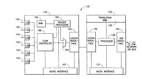
Figure 2 is high level block diagram of a destination
switch according to the invention.
Figure 3 is a diagram of a modified ATM cell including the
multicast session tag b~te according to a preferred embodiment of
the invention.
CA 022~3466 1998-11-03
W O 97/43867 PCTrUS97/09098
Figure 4 is a more detailed diagram of the multicast
indicator RAM of Figure 2.
DETAILED DESCRIPTION OF THE PREFERRED EMBODIMENTS
A typical ATM network 10 as shown in Fig. 1, includes a
network cloud 20 having a plurality of ATM switches 25, a
plurality of destination switches 30, and a plurality of ATM
terminals 40 which are coupled to the destination switches. Some
of the ATM terminals are shown having direct line connections 42
to the destination switches 30. Others of the ATM terminals are
shown coupled via a LAN 44 to the destination switches 30. An
ATM network controller 45 is provided for configuring the ATM
switches 25, 30, and for managing the network. Thus, the network
controller 45 typically provides each of the switches with
translation tables and other information which permits ATM calls
to be set up and to proceed. Those skilled in the art will
appreciate that many different network configurations are known
in the art; and Fig. 1 is a high level diagram provided by way of
example for background purposes only.
One of the well known functions of an ATM switch is its
capability of carrying out a multicast function; i.e., making
multiple copies of an ATM cell for delivery to multiple
destinations. As discussed above, recently there have been
proposals to provide destination switches with multicast
capabilities so that in a multicast situation, a single cell can
be sent to a destination switch having a plurality of terminals
coupled to it which are to receive the cell. In the prior art
proposals, the destination switch element must conduct several VC
address translations to locally multicast the cell to the
different terminals.
As seen in Fig. 2, and in accord with the invention, an ATM
destination switch 130 (which can be used in the network of Fig.
1 in lieu of switch 30) is provided which can locally multicast
ATM cells without conducting multiple VC address translations.
In particular, the ATM destination switch 130 typically includes
CA 022~3466 1998-11-03
W O 97/43867 PCT~US97109098
an ATM layer VLSI chip 132 and a physical layer VLSI chip 134.
The ATM layer chip, which is preferably a chip sold under the
tradename CUBIT (part #TXC-05801~ by the assignee hereof
TranSwitch Corporation of Shelton, CT, typically includes an ATM
interface 135, a processor 136, a microprocessor interface 137
and a UTOPIA interface 139. A translation RAM 138 is preferably
associated with the ATM layer chip 132. The ATM network
interface 135 (e.g., an eight bit UTOPIA standard type interface)
receives incoming ATM cells and forwards them to the processor
136. The processor 136 acts as a decoder means for decoding the
incoming ATM cell, among other things, to obtain a VPI/VCI, and
as a multicast session number assignment means for providing
additional routing information (i.e., a session number) based on
the VPI/VCI for the cell in order to permit the cell to be
multicast. In particular, upon decoding the VPI/VCI, the
processor (based on set-up information previously provided by
network controller 45) determines whether the incoming cell is to
be directed locally or switched for output to the network. If
the cell is to be directed locally, the processor provides the
ATM cell with additional routing information which is preferably
stored in the VPI/VCI translation table. As discussed
hereinafter in more detail with reference to Fig. 3, the
additional routing information is an index to a multicast
indicator RAM table located in the physical layer chip 134, and
may take the form of bits in an addltional byte or bytes added to
the cell header, or may take the form of one or more bits of the
existing five byte cell header.
It should be appreciated by those skilled in the art that
in certain embodiments of the invention, the processor 136 can
also act as a translation means for translating an incoming
VPI/VCI to a destination VPI/VCI (based on the translation table
in the translation table RAM 138). This capability is provided
in the CUBIT chip and is important for embodiments where the ATM
layer chip is connected directly to the ATM network, or is
coupled to the ATM network via a device or devices (not shown)
which do not conduct a VPI/VCI translation. However, in the
preferred embodiment of the invention, the CUBIT ATM layer chip
CA 022~3466 l998-ll-03
WO 97/43867 PCT/US97/09098
is connected to a CELLBUS (a trademark of the assignee hereof
TranSwitch Corporation) system (not shown) which includes
additional CUBIT chips and a backplane-type bus coupling the
CUBIT chips and which transports ATM bytes according to a frame
disclosed in co-owned U.S. Patent applications Serial Nos.
08/123, 881 and 08/213, 398 which are hereby incorporated by
reference herein in their entireties. In the CELLBUS system,
incoming ATM bytes undergo a VPI/VCI translation at the receiving
CUBIT chip, and the ATM bytes are then placed on the backplane-
type ~us for the destination switch of this invention. Thus,
upon the ATM layer chip 132 receiving the ATM cell from the bus,
the ATM cell already has a destination VPI/VCI, and no further
translation is required. However, as discussed above, additional
routing information for that destination VPI/VCI is provided by
the ATM layer chip 132 by the processor 136 (and utilizing the
translation RAM 138) in order to help effect a multicasting of
the ATM cell as discussed in more detail below.
The physical layer chip 124 of the destination switch
includes a UTOPIA interface 150, a demultiplexer 155, a header
processor 160, a multicast indicator RAM 162, a flow controller
166, and a plurality of ATM line interfaces 170 which are coupled
to ATM lines 142 and LANs 144. Additionally shown is a
microprocessor interface 167. After an ATM cell is provided with
the additional routing information to the UTOPIA interface 150 by
the ATM layer chip 132, it is demultiplexed by the demultiplexer
155 to provide the header processor 160 with the additional
routing information contained in the cell. Based on the session
index number contained in the additional routing information, the
header processor 160 accesses a corresponding location in the
multicast indicator ~AM 162 (the details of which are discussed
hereinafter with reference to Fig. 4) . Using the data contained
in the multicast indicator R~M 162, the header processor 160
directs the flow controller 166 to provide copies of the cell
(preferably without the additional routing information) to each
(one or more) interface 170 to which the cell is destined. In
this manner, where the cell is being multicast, the identical
cell (i.e., with the same VPI/VCI) is provided to the interfaces
CA 022~3466 1998-11-03
W 097/43867 PCTrUS97/09098
of multiple output lines, and may be buffered or otherwise
processed as necessary for output. During call set-up (in
accordance with known call set-up procedures which are not of
primary interest for this invention), the switch 130 will have
already informed each of the multiple destinations that a cell
having that particular VPI/VCI is destined for them. Thus, upon
seeing an ATM cell having the particular VPI/VCI, each of the
multiple users (whether on separate lines or on a LAN) will
receive the ATM cell.
The additional routing information is provided for all
cells which are to be terminated. According to a preferred
aspect of the invention, and as seen with reference to Fig. 3,
the additional routing information is provided as an additional
cell header "tag" byte to the standard fifty-three byte ATM cell.
For example, all eight bits of the tag byte of the now fifty-four
byte ATM cell will enable the destination switch to support two
hundred fifty-six local multicast sessions. Of course, fewer or
more bits or bytes can be used to support fewer or more multicast
sessions.
In accord with another embodiment of the invention, the
additional routing information is provided in the header of the
ATM cell. For example, the header error correction (HEC) byte of
the ATM cell, instead of being used for header error correction
may be used for the additional routing information. Thus, the
ATM cell would continue to include forty-eight bytes of data and
five bytes of overhead. Similarly, if one or more of the VPI,
VCI, and PTI were to be shortened (typically the VCI), the
additional routing information could be inserted in one or more
of those fields.
According to another preferred aspect of the invention, and
as seen in Fig. 4, the multicast indicator RAM 194 is an N x M
sized RAM, where N is the number of supported multicast sessions
(e.g., two hundred fifty-six), and M is the number of destination
switch output lines. With this arrangement, each of the N words
preferably assumes a position in the RAM associated with a
CA 022~3466 1998-11-03
W097/43867 PCT~S97/~098
session number. For example, the first word (0) is used to
correspond to session #0, while the second word (1) corresponds
to session #1. With N words, it will be appreciated that N
multicast communications can be simultaneously supported in the
switch of the invention. Within a word, the M bits of the word
are used as a binary bit map where the bit location is associated
with a specific output line (terminal). A "1" in the bit
location is used to indicate that the associated output line
should receive the cell, whereas a "0" indicates that the cell
need not be copied for that output. For unicast cells, only a
single "1" will appear in the word of M bits, whereas for a
multicast cell, a plurality of "1" values will appear in the word
of M bits.
It will be appreciated that the method of the invention is
closely related to the switch of the invention, and generally
includes: obtaining an incoming ATM cell, adding additional
routing information to the ATM cell, providing a table which
stores a multicast indicator, using the additional routing
information as an index to the table, and using the information
at the indexed location in the table to determine to which output
interfaces to provide the ATM cell.
There have been disclosed herein an apparatus and method
for providing multicast communication sessions in an ATM
destination switch. While preferred embodiments of the invention
have been described, it is not intended that the invention be
limited thereto, as it is intended that the invention be as broad
in scope as the art will allow and that the specifications be
read likewise. Thus, while the invention has been described as
being implemented in two VLSI chips (an ATM layer chip and a
physical layer chip), it will be appreciated that different
numbers of chips could be utilized. Also, while the ATM layer
chip was described as having a single ATM network interface, it
will be appreciated that multiple network interfaces could be
provided. Additionally, while the destination switch of the
invention was not shown as including a switch fabric, it will be
appreciated that the ATM layer chip could include or could be
CA 022~3466 1998-11-03
W O 97143867 PCT~USg7/09098
connected to a switch fabric. Furthermore, while the invention
was described with reference to standard ATM cells with a data
payload of forty-eight bytes and a header of five bytes, it will
be appreciated that the invention has application to any
telecommunications destination switch which is receiving cells
having a header and a data payload, regardless of the size of the
header and payload, and regardless of whether a single header is
used for a plurality of payloads such as for packet-type
communications.
Those skilled in the art will further appreciate that while
the invention was described as including a translation RAM in the
ATM layer chip, within the scope of the invention, for incoming
ATM traffic, it is not mandatory to conduct an incoming to
outgoing VPI/VCI translation; i.e., the incoming VPI/VCI can be
utilized as the VPI/VCI which is sent on the destination lines or
LANs to the terminals, or as previously disclosed, the VPI/VCI
translation could have been already carried out in another
apparatus. Furthermore, while the additional routing information
(session number) was described as being provided by the processor
of the ATM layer chip based on the incoming VPI/VCI, it will be
appreciated that the session number could be keyed to the
outgoing (translated) VPI/VCI; particularly where the VPI/VCI has
already been translated before being received by the processor.
Further yet, it will be appreciated that while the physical layer
chip was described as having a "header processor" block, a UTOPIA
interface block, a "flow controller" block, a demultiplexer
block, etc., these designations are for purposes of convenience
only. Thus, some or all of the blocks can be subsumed under
blocks of different designation such as "processor", provided
certain functions are provided: receiving the cell with the
additional routing information, using the routing information to
access a multicast indicator memory location, and forwarding the
cell to all line outputs indicated by the multicast indicator
memory location. Similarly, it should be appreciated that some
of the blocks described, such as the multicast indicator RAM, can
be located off-chip. It will also be appreciated by those
skilled in the art, that while the additional routing information
... . . . .. _ _ .. . . . . .
CA 022~3466 1998-11-03
W 097/43867 PCTAUS97/09098
is preferably stripped from the ATM cell before it is multicast,
the additional routing information can be maintained in the cell
being sent to the terminal equipment. In such a case, the
terminal equipment should be informed of the content format of
the cells being transmitted so that the additional routing
information will not be misinterpreted as data or other header
information. It will therefore be appreciated by those skilled
in the art that yet other modifications could be made to the
provided invention without deviating from its spirit and scope as
so claimed.