Note: Descriptions are shown in the official language in which they were submitted.
CA 022~3476 1998-11-03
WO 97/41923 PCr/US97/07572
Description
Imrl~nt~hle Carfli~ rdioverterlDefibrill~tor with Fl~I Suppression Filter
with In~ endent Ground
S
Technical Field
The present invention is directed towards an implantable biomedical device such as a cardiac
cardioverter-defibrillator, incorporating an output regulating circuit for controlling energy applied
to the heart and a sensing circuit for d~t~cting electrical conditions in the heart, and particularly to
filters for suppressing electro-magnetic hlle~relence (EMI) and the effects of defibrillation shocks.
B~rk~ground Art
The basic implantable cardioverter/defibrillator system consists of at least one electrode
attached to the heart and connected by a flexible lead to a shock or pulse generator. This generator
is a c~ billalion of a power source and the microelectronics required for the system to perform its
intended function. An implantable cardioverterldefibrillator may also include a p~cem~ker to treat
bradycardia. Many cardioverter/defibrillators in current use incorporate circuits and antennae to
communicate non-invasively with external instruments called programmers. Implantable
cardioverters/ defibrillators have the capability of correcting dangerous arrhythmias and fibrillation
by applying selected slim~ tion patterns or high energy shocks. High energy shocks are used
primariJy to correct life-thre:ltening fibrillations by e~.senti~lly stopping the heart and allowing an
apl.lol)~iate rhythm to re-establish itself.
To achieve reversion to an organized rhythm, it is generally believed that the heart should
receive an effective amount of electrical energy, equal to or exceeding a threshold energy. The
threshold energy may vary from patient to patient. Consequently, a physician will customarily
perform certain tests when implanting a defibrillator and will select an energy level for defibrillating
shocks. Implantable defibrillators are configured to deliver electrical energy by controlling the
voltage on or applied from output capacitors.
Implantable medical devices such as p:lrem~k~rs, defibrillators, and other implantable pulse
generators generally comprise one or more electrical leads in electrical communication with the pulse
generator which emanate from the housing and typically terminate at a distal location within the
patient. The leads transmit electrical signals to and from the device and, as such, are fabricated
having a conductor made from a metal alloy to enable good conductivity. Because of their
conductive properties, these leads effectively act as an antenna and thus tend to conduct unwanted
electromagnetic interference (EMI) signals. These EMI signals may be transmitted to the medical
_, .. . . . ... . . . . .. .
CA 022~3476 1998-11-03
WO 97/41923 PCTIUS97/07572
device and interfere with normal operations. Sources of EMI signals are prevalent and include, for
example, radio and TV transmitters, cellular telephones, medical electrosurgical equipment,
microwave devices, welding equipment, security and surveillance systems, and other sources of radio
frequency illt~lrele~lce (RFI). In implantable cardioverter/defibrillators, charging and delivery of
a defibrillating shock can cause EMI which adversely affects the sensing circuits or the operation of
the device.
Two basic a~-oaclles are employed to reduce the effects of u~ nted EMI on implantable
medical device operations. In the first approach, the medical device is enclosed in a metallic housing
or shield which may be conductively connected to a ground reference of the device. In the second
approach, a filtering circuit attenuates potential EMI before it reaches the circuitry of the medical
device. The two approaches may be used separately or combined.
Presently, multilayer ceramic type capacitors and, in particular, discoidal capacitors are
recognized as an effective alternative for filtering EMI. In a typical construction, these discoidal
capacitors form part of a feedthrough filter assembly, which admits patient connections through the
hermetic barrier of the device. The feedthrough assembly includes a metallic ferrule connected to
the capacitor and a terminal pin hermetically supported from and extending through the ferrule. The
metallic ferrule is connected to and hermetically sealed with the medical device. Typically, the
discoidal capacitor has two separate electrode plate sets which are embedded within a dielectric
substrate. One set of the electrode plates is electrically coupled to the terminal pin. This pin is
electrically connf cted at one end to the medical device circuitry and at another end to the lead used
to transmit the desired electrical signals to and from the patient. The other set of electrode plates
is electrically coupled to a cylindrically shaped ferrule which, in turn, is welded to the housing of
the medical device. Generally, the ferrule consists of a conductive material and may have an
in.c~ ting material disposed along an inner portion of the outer conductive surface. This insulating
material is used to support the terminal pin and rn~int~in it in nonconductive relation with the housing
of the medical device.
During signal tr~n.cmis.cion, the discoidal capacitor permits passage of relatively low
frequency signals along the lead, through the terminal pin, and to the medical device. Higher
frequencies, representative of the spectrum of unwanted EMI, however, are shunted to the housing
of the medical device by the capacitor and not permitted to pass into the medical device. As a
consequence, interfering signals which could otherwise adversely affect the performance of the
device are filtered as they enter the medical device.
Discoidal capacitors, as well as other multilayer ceramic capacitors, are formed of multiple
layers of alternating ceramic and metallic materials. Generally, the multilayer ceramics are available
CA 022~3476 1998-11-03
W O 97/41923 PCTrUS97/07572
in several different dielectrics and the choice of material depends on the desired capacitance volume
efficiency and the operating temperature range. Ceramic capacitors of this nature, however,
primarily serve to filter EMI and not protect against voltage transients and surges. For further
information regarding discoidal and multilayer capacitors, reference should be made to U.S. Pat. No.
5,333,095 by Stevenson et al., issued July 26, 1994, entitled "Feedthrough Filter Capacitor
Assembly for Human Implant", and Ivan G. Sarda and William H. Payne, "Ceramic EMI Filters -
A Review," Ceramic Bulletin, Vol. 67, No. 4 (1988), pp. 737-746.
Implantable defibrillators usually produce high voltage, high energy shocks by charging large
capacitors. It takes a certain amount of time, depending on the condition of the batteries and other
factors, to charge these high voltage capacitors. During this interval, it is possible that the heart may
spontaneously revert to a normal sinus rhythm. Since a defibrillation shock is both painful and
potentially dangerous, it is desirable to avoid delivering unnecessary shocks. To do this, implantable
defibrillators are programmed to continue to monitor the electrical condition of the heart during a
capacitor charging interval. If normal sinus rhythm is detecte-l, charging is interrupted and a shock
is not delivered. This is soml~times referred to as "continuous collfi.,llalion," m~ning that the
existence of a life-threatening tachycardia or fibrillation is constantly detected. It has been observed,
however, that the process of charging the high voltage capacitors can be so electrically noisy that the
heart's electrical signal cannot be reliably detected. This noise appears as internally-generated EMI,
tran.cmirted from high voltage leads or electrodes to a sensing circuit. It is desirable, therefore, to
reduce or eliminate this noise so that the sensing circuit can more readily detect the heart's electrical
slgnals.
Certain implantable cardioverter/defibrillators have been developed which deliver shocks
between an electrode mounted on a lead, preferably an endocardial lead, and a conductive part of
the hermetically sealed case or can C.~ i..i.,g the pulse generator. This is sometimes referred to as
a "hot can" and is analogous to so-called unipolar operation of a pacemaker, wherein a stin nl~ting
pulse is delivered between an electrode and a pacemaker can. The m~gnitude of a shock is, of
course, substantially greater than a pacing pulse and presents additional difficulties. In particular,
in a "hot can" implantable cardioverter/defibrillator with EMI filters, a shock waveform may be
prematurely terminated by a feedback effect. This appears to be attributable to the use of at least
two EMI Su~ g capacitor filters, between each pace/sense electrode, which may also be a high
voltage or shock electrode, and the can.
This phenomenon can be avoided by removing the EMI su~plessillg capacitor filters or by
substantially reducing their capacitance. This, however, renders the device more susceptible to
externally generated electromagnetic interference.
... .... .. . .
CA 022~3476 1998-ll-03
W O 97/41923 PCTAUS97/07572
It is an object of the invention, therefore, to provide an implantable cardioverterldefibrillator
in which the design of EMI suppressing filters is not influenced by the programmed selection of
shock delivery path.
It is a further object of the invention to provide an EMI filter configuration for an
implantable cardioverter/defibrillator which prevents premature termination of shock delivery.
It is another object of the invention to provide an implantable defibrillator which has
continuous confirmation, but which is not susceptible to charging noise.
Disclosure of the Invention
The present invention is addressed to an implantable defibrillator, which may include
cardioversion and pa~.em~ker capabilities, which has EMI filters which are not susceptible to
defibrillation shocks and which reduce or elirninate the effects of charging noise on sensing circuits
used for continuous confirmation. A first filter capacitor is provided between a sense electrode,
which may include pacing capabilities, and a ground reference within a hermetically sealed can
containing a pulse/shock generator. A second filter capacitor is provided between a pacing/sensing
reference electrode, which may also be a high voltage or shock electrode, and the ground reference.
In addition, there is a third filter capacitor between the ground reference and the can. Preferably,
the connections of the first, second and third filter capacitors are physically as well as electrically
adjacent to each other. In the preferred embodiment, the filter capacitors are housed in the can and
in or adjacent to a feedthrough assembly which passes through the can. Most preferably, the filter
capacitors are discoidal capacitors mounted in or adjacent to the feedthrough.
Bri~f Pescription of Drawings
FIG. 1 is a block diagram of an implantable pac.em~ker/defibrillator.
FIG. 2 is a block diagram of an output circuit for use in the defibrillator of FIG. 1.
PIG. 3 is a schematic diagram of a prior art EMI filter circuit.
FIG. 4 is a scl~m~tic diagram of an EMI filter circuit according to the invention.
FIG. 5 is a perspective view of a combined hermetic feedthrough and filter circuit according
to the invention.
FIG. 6 is a through section plan view of a first embodiment of the feedthrough and filter
circuit of FIG. 5.
FIG. 7 is a through section plan view of a second embodiment of the feedthrough and filter
circuit of FIG. 5.
FIG. 8 is a through section plan view of a third embodiment of the feedthrough and filter
circuit of FIG. 5.
Best Mode for Carryin~ Out the Invention
. ., . _ _ , .
CA 02253476 1998-11-03
~M 363 ~T
-5-
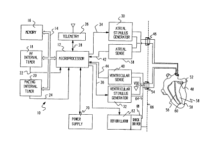
FIG I is a block diagrarn illustrating a rate adaptive pacern~rldefibrillator 10 according
t~ the invention. A micropr~cessor 12 preferably provides p.lcent~er control ~n~ ccmp\lta~ion~l
facilities. It will be appreciated that other form~ of circ~litry, such as analog or discrele digital
circui~ry c~n bc used in place ~f rnicroprocessor 12. Ho~ever, a microprocessor is preferred for
its miniature size and its tlexibility, ~oth of which are of critical importance in the imri~f~ble
systen~s in which it is envisioned the invention will find use. A particulally energy efficient
microproc~sscr ~hich i9 designed 6pecifically for use with imr~ t~le medical device~ i~ fuily
describdd i;l Gor~on, ~r ~1., U.S. Pa~ent N~. 4,404,g72, which i5 also assi~ned to the assignee.
l'he micmprocessor 12 has ~nput~output ports conr~ec~ed in ~ conventional rnanner via
bidirectinrlal bu~ 1~ t~ a n~ernory 15, an .~-V interva] timer 18, ~nd a p2~ing interval ~m~er 20. I~
~- addition. ~he A-V interval t~mer 18 and pacing inter-~a~ timer 20 each has an output connected
individually to a COr~eSpQlldiIlg input pQrtofthe mlcroprocess~r 12 by lines 22 and ~4 respecti~ely.
Memory 1~ preferably in~;ludes ~oth ~OM arld RAI~!~. The microproce~sor 12 m~y also
1 j contain ~ itionsl RG~f and RAhI as aescribed ~n the G~r~o~, e~ al. ~r.s. Pa~ent ~o. 4,404,~, 2.
~he paeema~er op rating rout~ne is stored in ROM The RA-~ stores v~rious prognrr~ le
parameters and l/~riables.
The A ~' and pac~ng inte~al timers 18 2nd ~0 may be ex~ernal to the rnicroproces~or I,, as
illustrate-l, or int~rnal thereto. as described in the Gordon, et al. U.S. Patcnt No. 4,~ 72. The
Jl~) hmess l~ 20 are suitable con~er~tional up or down counter~ of tlle type that are i~i~ially loaded with
a count value and count up to or down from the value and output a roll~ver bit upon co~pleting ~.e
pro~rarrlnled coun~. The initial count value is loaded ~Ilto the timers 18, 20 on bus 14 and ~e
respective rol~ ver bi~s are ~utput to t~e n~icroprocessor 12 on lines 22, 24.
The micro,~roces~or 12 preferably also has an input/output port cc)nrlecte~ to a telemetry
~5 lr.te.face 26 by IjLA~e f~O. ~hC de,~brill&tor, -w-hen impl~n~u, is ~us abie io receiYe pacing, arrhy~nmia
t~r~py, and rate controL parameters fr~m an ~xterIIal program~er and send data to an exterDal
receiver if desired. Many suitable telemetry s!~stems are known to those skilled in the arl. One ~u~h
syst m and encoding arrangernent is d~cribed i~.4r7nstrong a~d Co,~, U.S. Patent No. 5,3S3,91'
whi~ is al~o as~igned to the a~signee.
The ll,icr.~ uees~or output ports are &onn~t~d to inputs of an atrial sti~ulu~ pulse generator
30 and a ventricle stirn~lus pul~e generator 32 b~ ~ontrol lines 34 an~l 36 rcspectiYely. The
microprocessor I2 ~ansmi~ pul e para~neter data, such as arnplitude and width, as well ~s
enable/disable and puise initiatioxl codes to the g~ ators 30, 32 on the respec~iVe control lines. The
microproce~sor 12 also has input ports co~n~ct~d to outputs of an atr~al ~ensc amplifier 38 and a
~Ç~ 3 S~
o
K~ L. ~ t. ~ , r~J ~ J ~ J ~C~.~ . f~ I ~J
CA 02253476 1998-11-03
~ -36~CT -6-
venIricular sense a!r.pli~ier 40 by lin~s 42 and 44 respe~tively. Tbe ~tIial and ven~ricular scnse
amplifiers 3&. 10 detect elec~rical conditions irl the hea~t ~ncluding ~brill~tion and occurrences of P-
waYes ar~ R-waves. The atrial sense an~p'ifier 38 output~ a sigrlal on liIle 42 co the microproc~ssor
1~ whe~ ic de~ec~s a P-wave. This sign~l is latched to the microproces~or 12 input port by a
S conventional la~ch (r.ot ~houn) ~he ~entr.cular sense arnpl~fier 40 outputs a ~ignal on llne 44 to the
microprocessor 12 when it det~cts an R-wave. Thi~ signal ~s also latched tQ the microproce~sor 12
IrlpUt port by a conventional latch (not shown).
~he ~r~put of the atrial sense arnplifier 38 and the ourput of the atrial stirnulus pulse get~erat~r
30 are cormected ~ conductors through a first ~MT filter,ng feedthJorl,~h 4b, and through a
con~entional first lead 48 to a paticnt's heart ~0. Lead ~8 i~ inserted mto ~he pahent's heart 50
intra~e~ously or in ~.ny other suitabl~ 2~anner. The lead 4~ has an el~ctric,ali~ conduc~i~e
t~ pacing/sensing ~ip C2 or tip and ritlg at its dis~a' ~nd which is electric~lly colm~cted to the
conductors in lead 48. 'rhe paeingJsensing tip 52 is preferably lodged in ~he right atrlu~. Th~ u~
of the Yentricular sense ~rnplifier 40 and the ou~u~ of the ventricul~r s~m~lus pulse gener~or 32 are
onnec~ed b~ conductors Ihrough a second ~MT filtering ~eedthrou~h 54. ~e conduciors pais
chroueh a conventional se~ond lead 56 which is inset~ intrave~iollgly or otherwi~ in the right
Yentricle ~8 o~ ~he heart 50. Ihe second lead 56 has an electrically conductive p~cin~lser~ing tip
~0 or tip md ring at its dist~l end. The pacin~l~ensing tip 60 ;s eiecsricaILy connected to the
conductors in second lead 5~. The pacin~lsensing tip 6d IS pceferably lo~ged cn the ~all of ~he ri~ght
~0 ventricle ~8.
lhe conductors cond~lct the s~i2nullLs p~ses gener~ted by the atriaJ and ~~en~;ricular sti~lulus
pulse ~generators 30, 3~ to the pacing/sensing tips S~, 60. The paci~!sensing tips 52. ~a and
corresponding conductors al~o conduct cardiac electrical signals sensed in t~e right ~triurn ~d ri~h~
ven~ricle to the atrial ana ven~ricular ~nplifiers, 38, ~0 re~pectively, The sense amplifiers ~g, ~0
''5 enllaneelhe~ieC~riCai signais. Tn u~ preterred embod~ rxs ~f the inven~ion, the arnplifiers 38, 40
ha~ie an autornatic g3in cont~ol ~atNre, as described in U.S. Patent ~,903,699 1o Baker, er ~1. That
applicatisn is a~si~ned to the same assignee ~s tl~ present inve~tion.
T~e imrl~nt~ble cardiac stim~ tor 10 also ha~ a defibrillator ci~cuit 62. If fibrillation ~s
deteaed ~hrough the a~rial ~r ven~ricular sense amplifiers 38, 40, a high ener~y s~.ock can be
delivere~ ~hrough defibrill3.tion lead 6~ and elect~ode S6. De~ection algorithms for de~ection of
tachycardias and fibr .lation are described in Pless, et ~l., U.S. Patent 4,880,~05. Allh~ugh an
endocardi..l ~lectrod~ and use of ~he conductive part of th~ can or case are ~uggested by the drawin~,
pa~ch-type epicardial e~ectrodes ~or defibrillaliorl are al~o
AMENDED SHEET
,. . .. . ..
..... ~ ,.. . .
CA 02253476 1998-11-03
63Pc~
-7-
known. Tne shock is, contro!led l~y a shc~ck driv~er circuit 68, which will be more particularly
describ,ed herea~r A~l of the s~orementioned co~ponents are p~wered b~ a power sup~ly 70. The
po~er sup,uly 70 may comprise elther s~andard or rechargeable battcries or b~th. which ;nay b
dedicate,~ ~ the operation of different parts of the ~tirr~ r 10.
In the preferred embodiment of the inven~ion, it is considere~ d~sir,~ble to pro~uce multi-
ph,~,ic shocks for defib"llatiorl through the shock driver 68. Circuitry partlcu~arly v, el,' adapced for
producing such wave forms ir describe~ in detai~ in U.S. Paten~ ~c. 4.800,883 to W~nstrom.
Circu,~ry for the ~,hock driver 68 is sh~Jwn with greater particul,~-ity in PIG. 2. FIG. 2 illu~trates the
~hock drivcr 58 conr.eeted to the patie~'~, hear~ 50 through dle lead ~4 and el~ctrode 56 and througn
the call 66;~ produce a ~iph~sic w~e forrn, a b,~k of four three-ter~ninal semiconduetor sw~ches
72, ~4~ ?~ sueh as ir~ulated g~te bipolar trans~tor (rGBri switches, rnay ~e empl.~ d. It wiil
~_ be unders~ood, however, tt~t the invention can ~e emplo~ed with mo~opl~sic ~ulse gener~tors and
~ith p-~lse generator~, incorporating rn~1~tirh~cic ~tim~ orl~ The switches 72, ?~ " 78 are
c~ntrolled hy drivers 82, 84, 86, 8~ respectively. The drivers 82, 84, 86, 88 a~e c~n~rolLed by
~5 command puises from the miCrroproceggor L2 through control lines 80 ~nd 91, as will De snore
particular~y dcscrlbed below. The energy to pr~duce bi~hasic defi~ri!1arng shocks is ~plied from
high vol~age capacitor 92. High volt~ge capacitcr 92 is conn~te~ to swi~ches, 2 and 7~, and c~Lrrerlt
therefrotn returns ~ ia switches 76 or 7~. The first leaà 64 is cnnnPrte~ beeween switche~ 72 and 76
wniie the second lead 66 i~ connected berween switches 74 and 78.
2n ~ amount o~ energy deliver~d to t}~e heart is de~endanl upon ~e voltage on the high
voltage c~acitor. rhe voltage appearirlg OII the capaci~ot 9~ i5 controlled by voltage c~ntroller 9
which is coanected to ~ source of power s~lch as the battery or po~er supp1y 70 through line iO0.
The voltage controller 9~ ls controlled t~ro~lgh a line 1~4 from the microproc~ssor I2. This
-~ configuIation is described in more detaii in Lhe ~i~trom patent rnen~ione~ above. In ~he
'~ CO~fij~,'Ula;iOrl ~hUWl~ t~ pro~ucc a ~Lnidirectionai current pulse ~hrou~h the heart 50, the
m~croprocessor 12 issues a c~lnrnand along lLne 8~) to drivers 82 and 88, closing ~v~tches 72 ar~d 7~.
Both be~or~ and ~er the comrnand, all ~witches are normally opened. To produce ~ opposite
currerlt, the microprvcessor !2 issues a command on line 90, clo~ir4 cwitches 84 and ~6 and
directing ~;he curren~ flow in the oppo6ite direction through the heart 50.
The EhlI fiiter according to ~he in~entton will now be descr~bed. A prior art EMI ~Iter 90
i~ illussra~ ,;n FIG. 3. Such a filter 90 migkt be comprised ~f discrcte con~ponents, or incorporated
into a set of discoid~l capacitors. Such di~c~ capacitors m~gh~ be mounted in a feedthrvugh such
as feedthrough 54. or adJacen~ the feedthrough, as described jTl St.~pher~,on et al. U.S. PateM
AMEN~D SHEEt
. ..... , , , ".. ,, ,, ,, ,, ~, .. .
CA 022~3476 1998-11-03
W O 97/41923 PCTrUS97/07572
5,333,095. Fundamentally, an EMI filter 90 comprises a lead 92 which would pass through a
desired case such as the can 66 to provide an electrical connection through the can 66. The lead 92
might, for example, be connected to the ventricular sense circuit 40 and the ventricular stimulus
generator 32 within the can at pin l and to the tip electrode 60 outside of the can. A first capacitor
94 is connected from the lead 92 to the can 66 to provide a high frequency path for EMl. Multiple
leads and capacitors could be provided in a single configuration or at a single feedthrough. For
example, as shown in FIG. 3, an additional lead 96 could be provided within an associated capacitor
g8 connected from the additional lead 96 to the can 66. Pin 2 of lead 96 might be connected, for
example, to the shock driver 68 within the can and to the endocardial electrode 70 outside of the can.
In an implantable cardioverter defibrillator, charging noise is generated during the process
of charging the high voltage capacitors in the defibrillator 62 prior to shock delivery. Charging noise
may be present as an electric field coupling from the can or by induction of eddy currents. This
sometimes occurs when a "hot can" electrode has been introduced into the shock delivery pathway,
that is, when the can 66 is used as one of the electrodes. The prior art connection of the C 1 and C2
capacitors 94, 98 respectively, directly to the can 66 can cause an inappropriate sensing during the
charging cycle and premature termination of a can-delivered shock. Even if two or more
defibrillation electrodes remote from the can are used, charging noise can still prevent a sensing
circuit from detecting the electrical condition of the heart, if continuous confirmation of the life-
threatening condition is attempted. These situations are avoided by the configuration of the invention
illustrated in FIG. 4.
FIG. 4 illustrates an EMI filter 100 according to the invention. The EMI filter 100
comprises at least one lead 102, configured to pass through the can 66. As before, this lead 102
might be connected within the can at pin 1 to the ventricular sense circuit 40 and the ventricular
stimulus generator 32. Outside the can 66 the lead 102 might be cormected to the ventricular tip
electrode 60. A shunt capacitor 104 is provided similar to the capacitor 94 described above.
However, instead of being connected to the can 66, this capacitor is connected directly to the internal
system ground 106. A C3 capacitor 108 is connected between the common contact of the Cl
capacitor 104 and of the system ground 106 and the can 66. In the preferred embodiment, the
capacitance of the C I capacitor and the C3 capacitor are approximately equal. Charging noise is
generally within the frequency range of 100 kHz to 200 kHz. Consequently, the Cl capacitor is
chosen to easily pass freql~Pn~ies higher than 100 kHz. These frequencies are passed directly to the
system ground since it passes tllrough but a single capacitor. This adequately (limini.~hes the effect
of charging noise on the circuit and prevents improper sensing. On the other hand, external EMI
generally consists of frequencies in excess of 1 MHZ. These frequencies are passed easily through
.., .. ~ ~ .. . ..
.. , . . . , . .. ~ ~
CA 022~3476 1998-11-03
W O 97/41923 PCTrUS97/07572
the capacitor C1 and C3 in series and are diverted to the can. External EMI entering either from
the tip electrode 60 or the endocardial defibrillation electrode 70 needs to be ~tteml:~ted before it can
be demodulated by the rectifying properties of semi-conductor junctions. This is done by .~hllnting
the EMI currents back to the can which acts as a Faraday Cage for the device. The C3 capacitor 108
S provides a low impedance path from the ground reference to the can. Multiple leads may be
provided through the can, either electrically a~j~rent, or both electrically and physically adjacent one
another. For example, an additional lead 110 could be provided to connect to the endocardial
defibrillation electrode 70 and through pin 2 to the shock driver 68. A C2 capacitor 112 is connected
from the lead 10 to the system ground 106 and to the C3 capacitor 108.
0 The EMI filter 100 of the invention may be provided as separate components connected to
a standard feedthrough. However, the preferred embodiment is to construct a feedthrough and EMI
filter as a common feedthrough structure 114 as illustrated in perspective view in FIG. 4. The
feedthrough structure 114 comprises the leads 102 and 110 described above and a system ground
connection 116 for connection to the system ground 106. The leads 102, 110 and 116 are embedded
in a feedthrough 118 having a metal ferule 120 for connection to the can 66 which houses a capacitor
structure 122. The capacitor structure 122 may be constructed in a variety of ways, as will IIOW be
explained.
One embodiment is shown in FIG. 6, which represents a plane through section of the
feedthrough system 114 of FIG. 4. As seen in FIG. 6, the metal ferrule 120 of the feedthrough 118
has a circumferential groove 124 for receiving the can 66. A hermetic seal 126 plugs one end of the
feedthrough 118 around the leads 102 and 110. Such hermetic seals are known in the art, and are
described, for example, in U.S. Patents 3,920,888 and 4,678,868. The capacitor assembly 122
comprises chip capacitors employed for the capacitors 104, 112 and 108. The shunt capacitor 108
is connected by a jumper 128 to the metal ferrule 120. Alternatively, the jumper 128 could be
connected directly to the can 66.
An alternative construction comprised of discoidal capacitors is illustrated in through section
in FIG. 7. As in the embodiment of FIG. 6, the leads 102, 110 and 116 and the metal ferrule 120
and hermetic plug 126 are substantially as described above, and perform the same functions. Instead
of the chip capacitors, however, the capacitors 104, 108 and 112 are comprised of discoidal
capacitors. In particular, the ground line 116 which is intended to be connected to system ground
106 is connected to an annular ring conductor 130. Plates on the outside of this ring 130 interleave
with plates connected to the ferrule 120, thus forming the shunt capacitor 108 which connects to the
can through the ferrule 120. On the inside of the annular conductor 130, additional plates h1terleave
with plates connected to the lines 102 and 110 to form capacitors 104 and 112 respectively
CA 022~3476 l998-ll-03
W O97/41923 PCTrUS97/07572
-10-
A third embodiment is illustrated in through section in FIG. 8. As in FIGS. 6 and 7, like
numerals indicate like parts. In this embodiment, however, the capacitors 104, 108 and 112 are
formed as individual stacked discoidal capacitors formed adjacent their respective leads 102, 116 and
110.
Each of the embodiments of FIGS. 6, 7 and 8 are shown with the capacitor structure 102
contained within the ferrule 120 of the feedthrough 118. However, the invention could also be
implemented using discoidal capacitors attached around the ferrule, as shown, for example, in
Stephenson et al. U.S. Patent 5,333,095.