Note: Descriptions are shown in the official language in which they were submitted.
CA 02253610 1998-11-04
WO 97/43730 PCT/US97/07967
ALIG~MEN~r bI~T~IOD A~D ~PPARATUS FOR RETRIEVING lNFORMATION
FROM A TWO-DIME;NSIONAI. DATA ~RR~y
1.0 B~CE~GBOIJND OF THE INVENTION
c~Lon cnnr~r~ - 6y9tem8 for optically 6tori~ Imd r~Lri~c~lg data ~tored 89 li~lt
rl~e~i~e char. - ic~iro on an optical m~t ~1 ~md providing fast random aCCe98 retr~- .al. and
more particula~ly~ to an slie~m~nt method and apparatus sensine an optical unsge of the daL~
and LO~ ting same to ol~ data sienal~.
Optica} ~ ~~ of the type haviAg large J~m~ nt~ c~f dig~tal data ~ed by li~ht
modifging chanet~rio~irq of a ~ilrn or thin laycr of mP~eri~l snd ac~FFed by optic~l light
adL~...g ~nthout rnDr~Pn~ o.~cnt }~ave been pro~se~ but have not r~s ~It~d ir~ wide
sprcad con-mPrcial ~ vst;~n The interest in ~uch optical recor~g and ,d.;c.sl terhn~ogy is
due to its record tensity and faste~ ~h;~ l of large ~mo~n~ of data compared to that of
o~cisting electro-optical ~snie_$ such as optical d~scs, snd m~el~PtiC ~torap fill~ih a~ tspe and
moeTl~tic~ diSC, 811 of wbich requ~e relati~re mo~ion o~ the ~torage ~e~
For PY~m, ~e, ~ the c~;e of optical di6c memories, it is nFce~r~ to _,pin the record and
mow a read head radia~ly to ~e .~, the data, which is output in serial f~iAn The serial
~ of data g~.r~rUl~y requi-~s trz~ncfier to a ~uffer or solid ~tate random acce~s memory of a
data pL~ in order k~ e ~ m~7Ao~e high 6peed da~a ~dressing and other ~ata operations of
~ rr. computers. Other storage de~ices such as wlid state ROM a~ld RAbI can provide t~e
rdstively high acce-s ~peeds thst are sought, ~ut the co~t, size, and heat ~ p~tjAA o~ 6uch
devices whe~ r~ird to relatively lare- data cs~- t:-e ~im~t their ~r~liAo~
~ aA-pl~ of-~orts to pro~ide t}~e relatively large capacity s~orago a~d f~t access of an
optical memory of t~e ~ype t~at is ~e 6ubject of this invention are ~lirA~o~Ae~ in t}~e patent
lit~ t.. . e ~ a~ U.S.. Patent 3,806,643 fo~ PHOTOG~APHIC RECO~)S OF I)IG~TAL
I~RMATIO~ AND PLAYBACK ~Y~l~S INCL~lNG OPTICAL SCAN~ and U.S.
Patent 3,885,094 for OPrICAl, SCANNE:R, both by J~ne~ T. R~ 1 U. S. Pate~t 3,898,005 fo~ a
HIGH I)E~SITY OPTICAL MEMORY M~ANS ~;MPLOYI~G A MULTIPLE LE~S A~AY; U. S.
SUBSmUlE SHEET (RULE 261
CA 022~3610 1998 - l l - 04
WO 97/43730 PCT/US97/07967
Patent No. 3,996,570 for OPTICAL MASS MEMORY, U. S. Patent No. 3,656,120 for READ-
ONLY MEMORY; U. S. Patent No. 3,676,864 for OPTICAL MEMORY APPARATUS; U. S. Patent
No. ~,899,778 for MEANS EMPLOYING A MULTIPLE LENS A~RAY FOR READING FROM A
HIGH DENSITY OPTICAL STORAGE; U. S. Patent No. 3,765,749 for OPTICAL MEMORY
STORAGE AND RETRIEVAL SYSTEM; and U. S. Patent No. 4,663,738 for HIGH DENSITY
BLOCK ORIENTED SOLID STATE OPTICAL MEMORIES. While some of these systems
attempt to meet the above mentioned objectives of the present invention, they fall short in one or
more respects.
1.1 SUM~ARY OF THE INVENTION
In a system for storing and retrieving data from an optical image containing twodimensional data patterns imaged onto a sensor array for readout, method and apparatus
provided for detecting and compensating for various optical effects including translational and
rotational offsets, magnification, and distortion of the data image as it is converted to electrical
data by the sensor array. Data may be stored for example in an optical data layer capable of
selectively altering light such as by changeable transmissivity, reflectivity, polarization, and/or
phase. In one embodiment using a transmissive data layer, data bits are stored as transparent
spots or cells on a thin layer of material and are illuminated by controllable light sources to
project an optically enlarged data image onto an array of sensors. Data is organized into a
plurality of regions or patches (sometimes called pages). Selective illumination of each data page
and its projection onto the sensor array accesses the data page by page from a layer storing many
pages, e.g., of a chapter or book. The present invention may be used in optical memory systems
~ described in U.S. Patent No. 5,379,266, Patent No. 5,541,888; international application nos.
PCT/US92/11356, PCT/US95/04602, PCT/US95/08078, and PCT/US95/08079; and copending U.S.
Application SN 08/256,202, which are fully incorporated herein by reference.
The sensor array may be provided by a layer of charge coupled devices (CCDs) arrayed in
a grid pattern generally conforming to the projected data page but preferably the sensor grid is
S~mewhat larger than the imaged data. The data image generates charge signals that are
CA 022~3610 1998 - l l - 04
WO 97/43730 PCT/US97/07967
outputted into data bucket registers underlying photosensitive elements. Alternatively, other
output sensor arrays may be employed, including an array of photosensitive diodes, such as PIN
type diodes.
Systems of the above type and other devices in which optical data are written ordisplayed as two-dimensional data patterns in the form of arrays of cells, symbols or spots,
require a process or logical algorithm, implemented in hardware and/or software, to process
signal values from sensor elements in order to locate and decode the data. In general, there will
not be a direct correspondence between a sensor element or cell and a binary "zero" or "one"
value. Rather most data encoding techniques will result in a local pattern of sensor cell values
corresponding to some portion of an encoded bit stream. In all but the least dense codes, each
sensor cell value must be interpreted in the context of the neighboring cell values in order to be
translated to one or more bit values of the encoded data. The specific embodiment described
below is referring to On Off Keyed (OOK) encoded data. A simple example could use a
transparent spot in the data film layer to represent a "one" value, while an opaque spot would
correspond to a "zero" value. If the two-dimensional data array in question is a data pattern,
optically projected onto a grid of an optical sensor (for example, a CCD camera), and the data
pattern overlays and aligns to the sensor grid in a prescribed manner, there are five modes in
which the data can be misregistered. These misregistrations may occur singly, or in combination,
and manifest themselves as:
X axis and Y axis displacement error
Focal (Z axis) error
Rotational error about an origin
M~gnific~qtion error
Distortion
Focal (Z axis) misregistration can be minimi7.ed by careful optical and mechanical design
as is done in the embodiment disclosed herein. In addition to misregistrations, the imaged data
may be contaminated by electrical noise, by optical resolution limits and by dust or surface
contamination on the data media and/or optical sensor.
, . .
CA 022~3610 1998 - l l - 04
WO 97/43730 PCT/US97/07967
Although it is possible to compensate for linear misregistrations by mechanical methods
such as sensor stage rotation, or mel~h~nic~ Y axis) translation, it is often not desirable to do
so because of mech~nic~l complexity, cost, and speed constraints. Nonlinear misregistrations are
considerably more difficult, if not impossible, to correct me~h~nic~lly. Similarly, it is usually not
5 possible to compensate for random contamination by me-~h~nic~3l means alone, but such
contamination can be substantially compensated for by use of known error correction codes
(ECCs).
In accordance with the preferred embodiment of the present invention, raw image data is
sensed on a grid larger than the page image and then electronically processed to determine the
10 true data corrected for displacement, rotation, magnification and distortion. The processed,
corrected data is then output to memory or throughput to applications.
In the preferred embodiment, the sensor structure is a two-dimensional array of larger
area than the two-dimensional data image projected onto the sensor array, and the individual
sensor elements are smaller and more numerous (i.e., denser) than the data image symbols or
16 spots in order to oversample the data image in both dimensions. For example, two or more
sensing elements are provided in both dimensions for each image spot or symbol representing
data to be retrieved. About four sensing elements are provided in the disclosed embodiment for
each image spot, and intensity values sensed by the multiple sensor elements per spot are used
in oversampling and correction for intersymbol interference. Each page or patch of data is
20 further divided into zones surrounded by fiducials of known image patterns to assist in the
alignment processes and gain control for variations of image intensity. In carrying out these
operations, the analog level sensed at each of the oversampling sensor elements is represented by
a multibit digital value, rather than simply detecting a binary, yes or no illumination. The
preferred embodiment includes automatic gain control (AGC) of image intensity which is initiated
25 outboard of data zones by using AGC skirts of known image patterns and AGC peak detection
circuit processes to track the image intensity across the entire plane of each data zone. The peak
detection process and associated circuitry preferably uses a two-dimensional method that
_ _
CA 022~3610 1998-11-04
W097/43730 PCT/US97107967 -
averages a baseline signal of amplitude along one axis and a linear interpolation of the peak
detection amplitude along the other orthogonal axis.
Additional features of the preferred embodiment include the provision of alignment
fiducials containing embedded symbols of known patterns and positions relative to the zones of
data symbol positions, and the fiducial patterns have predetermined regions of maximum light
and dark image content which provide periodic update of the AGC processes summarized above.
Using these processes, a coarse alignment method determines the approximate corner locations of
each of multiple zones of data and this is followed by a second step of the location procedure by
processing corner location data to find a precise corner location. Preferably, the precise or fine
corner locating scheme uses a matched filter technique to establish an exact position of a
reference pixel from which all data positions are then computed.
Alignment of the data to correct for various errors in the im~ging process in the preferred
embodiment uses polynomials to mathematically describe the corrected data positions relative to
a known grid of the sensor array. These alignment processes, including the generation of
polynomials, make use of in-phase and quadrature spatial reference signals to modulate to a
baseband a spatial timing signal embedded in the alignment fiducial which is further processed
through a low pass filter to remove the spatial noise from the timing signal. In this manner, the
combination of in-phase and quadrature spatial reference signals generates an amplitude
independent measure of the timing signal phase as a function of position along the fiducial.
To generate the polynomials that determine the correct alignment of data based on the
alignment fiducials, the preferred embodiment uses a least squares procedure to generate the
best fit of a polynomial to the measured offsets. The coefficients of the polynomials are then used
- to derive alignment parameters for calculating the displacement of data spot positions due to the
various mis~lignment effects due to the optical, structural, and electrical imperfections. As a
feature of the preferred processing, second order polynomial fit information is employed to
estimate the optical distortion of the image projected onto the sensor.
.
CA 022~3610 1998 - l l - 04
WO 97/43730 PCT/US97/07967
After alignment the recovered image information is further refined by using a two-
dimensional pulse .qlimming process in the preferred embodiment to correct for two-dimensional
intersymbol interference.
The sensor employs a broad channel detection architecture enabling data of exceptionally
long word length to be outputted for use in downstream data processes.
1.2 BRIEF DESCRIPTION OF THE DRAVVINGS
The foregoing and other features of the present invention will be more fully appreciated
when considered in light of the following specification and drawings in which:
Figure 1 is a block diagram of the ORAM system in accordance with the preferred
embodiment.
Figure 2 shows illustrations of data media at different magnifications to show the break
down of the data hierarchy from a "chapter" into "patches" (also called pages), and a "patch"
(page) into "zones" and "zones" into data symbols or spots.
Figure 3 shows a portion of a data pattern portrayed as rotated, translated, andsomewhat distorted with respect to the orthogonal sensor co-ordinates (three of the several forms
of image defects which the method corrects).
Figure 4 is an illustration of a patch with an exploded view of a corner region containing
a corner symbol, two AGC "skirts" and portions of two alignment fiducials.
Figure 6 is a flow diagram overview of the sensor and alignment/bit retrieval process.
Figure 6 shows data patches before and after AGC.
Figure 7 illustrates an image of a patch showing the two sets of AGC skirts.
- Figure 8 shows a comparison of possible paths for AGC analysis, when centered on the
AGC skirt, the AGC process can analyze a known pattern.
Figure 9 is a diagram of a sensor array with a patch image projected on it, showing how
26 the sensor is divided into six sections for analysis.
Figure 10 shows the process for finding the center of an AGC skirt.
CA 02253610 1998-11-04
WO 97/43730 PCT/US97/07967
~i~re 11 is 8 diagram of how AGC normalizes intensity of the patch image. i11ustrating
that in the rea~out direction, the A to D converter threchold~ are set by the peak snd valley
~eeti~n circuitry, and in the lateral direction, linear interpolation i~ used to set the thr~ olds
Figure 12 is a diagram of a patch showing the reg~on~ of the patch a~socIated with the
~ree modes of AGC o~ L;~
Figure 13 shows a section of 6ensor image ~ie~ljehtir~g 8 corner r~gion, corner symbol,
and spot or pixel in the corner u9ed as an on~in for ~f~re~.clng positio~s of nearby data symbol~
. or spot~.
~igure 14 S~OW9 the AGC ~l~irts and corner ~ymbo}s purposely aligned ~uch that the row
and col~mn pocitinns of the AGC sl~irt cenbrs can be cQInhin~d into coo~ a~e pa}rs which
~eccme a coarse mea~ ement of the corner 6ymbol locations,.
~igure 15 is a flow chart of the corner symbol convolution process.
Figure 16 is a fragmer~t of th~ data image at the sen~or 3~0wing one of the zones with
corresponding fiducials including corner 6ymbo~s.
1~ ~igure 17 is a now chart of the data s~ m~nt process.
Eigure 18 illustrates the rl~çen~nt of the filters on the ~ nm~nt fiducials.
Figure 19 shows the typical curve for phase in x~direction as a function of x (8ssuming ~o
noise).
I~ure 20 ~bo~s Yalues for phsse in x direction a6 a function o~ x (including noise).
Figure 21 shows values f~r phsse in y-dire~tion as 8 function of x (inrlucling noi~e).
Figure 22 ~hows linear (first order~ fit to phase v~lues.
Figure 23 shows ~uadratic (~econd order) fit to phase values.
Pi~ure 24 i~ a diagram illu~trat~g the labeling of the four fiducials 6u~0unding a zo~e.
F~gure 25 is Bn eye disgram showing t~e ef}ects of noi6e, data spot interpolation snd
p~se Slimmir~,~
- Eigure 26 illllstrates the relation~hip betweeI~ sym1Dol po6ition on pixel array versus the
weighting value~ used for interp~at~
CA 022~3610 1998-11-04
WO 97/43730 8 - PCT/US97/07967
Figure 27 shows the 16 regions of symbol position on the pixel and the corresponding
pixel weights used for interpolation.
Figure 28 shows the ORAM electronics receiver subsystem including sensor integrated
circuit ~IC).
Figure 29 shows relative pixel magnitude for single and grouped "ones".
Figure 30 is a functional block diagram of the sensor IC.
Figure 31 shows an AGC skirt layout.
Figure 32 shows A to D codes with respect to signal intensity.
Figure 33 shows the signal flow on the sensor IC of Figure 30.
Figure 34 shows an alignment-bit-retrieval (ABR) IC block diagram.
Figure 35 depicts the segmented memory design of the ABR IC.
Figure 36 shows the 8 word adder and accumulator function.
Figure 37 shows the zone in image memory.
Figure 38 shows related diagrams illustrating the interpn;ation and pulse ;~limming
technique.
Figure 39 is a diagram of the output RAMl buffer.
~igure 40 is a timing diagram from re~uest to data ready access.
2.0 INTRODUCTION TO DETAILED DESCRIPTION
An image of a two-dimensional data array is formed on an optical serlsor. .L'tored digital
data is to be recovered from this image. A representative two-dimensioilal mernory device to
accomplish this data recovery is deEcribed in US Patent number 5,3'l9,266, "Optical Random
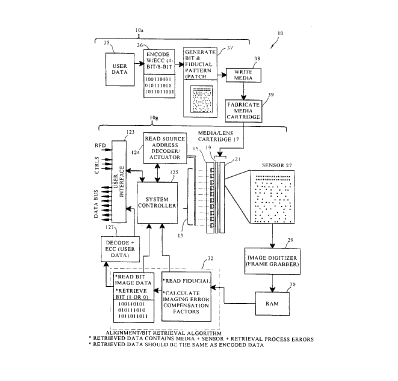
- Access Memory," (ORAM) and Figure 1 shows a functional block diagram of an ORAI\~ system 10
suitable for disclosing the alignment method and apparatus of the present invention.
ln the embodiment of Figure 1, a record is made as indicated at 10a, in which user data
is encoded combined with fiducials in data patterns called patches or pages that are written onro
record media 19. More particularly, and as fullr disclosed iIl copending applicaf;ions
PCT/US92/113Ofi and ~SSN 08/256,202, user data is entered at 35, encoded/ECC at 3.;,
, . . ..
CA 022~3610 1998-11-04
WO 97/43730 9 PCTIUS97/07967
whereupon data and fiducial patterns are generated 37, and written at 38 to media, such as an
optical data layer capable of selectively alternating light in one or more of the above described
ways. The data layer 19 thus prepared is then fabricated at 39 in combination with a lens array
21 to form media/lens cartridge. In this example, the image of a two-dimensional data field, as
5 written by E-beam on a chromium coated quartz media substrate. To retrieve the data from the
record, the media, lens cartridge 17 is removably placed in an ORAM reader indicated at 10b and
the data from each patch or page is selectively back-illuminated so as to be projected onto a
sensor 27.
An individual page or "patch" of data is back-illuminated when data in that patch is
selected at 124 via a user data request provided at interface 23 as described in U.S. Patent No.
5,379,266. More specifically, system controller 125, as described in the above-mentioned pending
applications PCT/US92/11356 and SN 08/256,202, coordinates the operations of a read source
124, alignment/bit retrieval processor 32, and decode and ECC 127. A lens system focuses the
image onto a sensor array 27 which converts light energy into an electrical signal. As described
more fully below, this signal is first sensed by analog circuitry, then converted to a digital
representation of the image. This digital image representation is stored in RAM 30 whereupon it
is operated on by the retrieval algorithms processor indicated at 32. The digitized image is
processed to correct for me-~h~ni~zll, electrical, and optical imperfections and impairments, then
converted to data and ECC at 127, and the data presented to the user via user interface 123.
In the representative ORAM 10, the symbols (or spots) making up the pages of the record
are disclosed in this embodiment as bits of binary value; however, the invention is also useful for
non-binary symbols or spots including grayscale, color, polarization or other changeable
characteristics of the smallest changeable storage element in the record. These available symbol
locations or cells are placed on a 1 micron square grid. Logical "ones" are represented by
optically transparent .9 micron holes formed in an otherwise opaque surface, while "zeroes" are
represented by regions that remain opaque (unwritten.) Symbols are grouped into "zones" of 69
by 69 symbol positions with 21 zones grouped to form a unit of data defined as a "Patch."
CA 022~3610 1998-11-04
WO 97/43730 10 PCT/US97/07967
Multiple patches comprise the unit of data defined as a "Chapter." Chapters comprise the unit of
data contained on a single removable data cartridge 17.
- Media layout architecture is depicted in Figure 2.
Using the method described herein, there need be no predetermined, fixed registration,
alignment, or m~gnific~tion of the data array image with respect to the sensor pixel array. The
two requirements for the sensor array are (1) that it be somewhat larger in both X and Y
dimensions than the image projected on it to allow for some misregistration without causing the
data image to fall outside the active sensor region, and (2) that it have a pixel density in both the
row and column dimension which is greater than the density of the projected symbol image so as
to be sufficient to recover the data, and in this embodiment it is approximately twice the symbol
count projected on it. (The sensor hardware design providing this function is detailed in Section
4.1.) The alignment method described in this disclosure will:
locate the image data array on the sensor,
~ determine the position of each individual data symbol in the image relative to the
known sensor grid, and
determine the digital value of each bit.
A fundamental purpose of the herein disclosed alignment method and apparatus is to
determine the spatial relationship between the projected image of the data array and the sensor
array. The grid of the sensor array is formed by known locations of the sensing cells or elements
which are sometimes called pixels in the following description.
Each zone is bounded on the corners by "corner symbols" and on the sides by alignment
"fiducials." The function of the corner symbol is to establish an origin for analyzing the fiducials
- and calculating symbol positions. The fiducial patterns themselves are used to calculate the
"alignment parameters."
This disclosure describes the method and apparatus for Steps 2 through 8, collectively
called "alignment and bit retrieval" (ABR). Steps 1, 9, and 10 are included for completeness.
CA 022~3610 1998-11-04
WO ~7/43730 11 PCT/US97/07967
The lo~ical functions associated with each step in Fi~ure 5 are summarized on the
followin~ pa~es:
3.1. STEP 1: DATA REQUEST
A user request for data initiates an index search in RAM to determine the address of the
5 patch(es) containing the desired data. The light source serving this data address is ilhlmin~ted,
projecting an image of the desired data through the optical system and onto the sensor. This
image, projected on the sensor, is the input data for the alignment and bit retrieval apparatus.
3.2. STEP 2: READ SENSOR AND PERFORM AUTOMATIC GAIN CONTROL (AGC~
The goal of the AGC process is to normalize the intensity profile of the patch image and
10 to adjust the analog thresholds of the A/D conversion so as to efficiently spread the range of
analog values associated with the modulation depth over the available levels of digital
representation. Figure 6 shows two images. The image on the left is of a patch as detected
before the AGC process. The image on the right is of the same patch after AGC has been
performed.
Automatic gain control (AGC) is the process of modifying the gain of the amplifiers which
set the threshold values for the analog to digital converters (ADCs). The term "automatic"
implies that the gain adjustment of the amplifier "automatically" tracks variations in the image
intensity. As image intensity increases, amplifier gain increases, and as image intensity
decreases, amplifier gain decreases. The effect of AGC is to provide a digital signal to the
analyzing electronics which is approximately equivalent to the signal that would be derived from
an image with a constant intensity profile over the entire sensor. The closer the resulting
normalized signal approximates a constant intensity profile, the lower the signal to noise ratio at
which the device can operate without error. AGC is necessary because image intensity may vary
across the sensor due to many causes, including:
Variability in the illuminating light within the optical system,
Low spatial frequency variation in symbol transmittance or pixel sensitivity.
Amplifier gain is set based on the intensity read from predetermined "AGC regions"
spaced throughout the data pattern. There are two types of AGC regions:
CA 022~3610 1998-11-04
WO 97t43730 1 2 PCT/USg7/07967
a) AGC "Skirts" located on the perimeter of the data patch. "AGC Skirts" are the
first illuminated pixels encountered as the array is read out. They provide an
initial measure of intensity as image processing begins.
b) AGC "marks" located in the alignment fiducials along each side of each data zone.
AGC marks are used to update the amplifier gain as successive rows are read out
from the sensor array.
As pixel values (the value of the light image falling on a sensor element) are read from
the sensor array, the AGC skirts are used both to predict the locations of the AGC regions on the
image plane and to set the initial gain of the ADCs. This is completed prior to processing the
10 pixels corresponding to data symbol positions on the image. Figure 7 depicts an entire patch of
21 data zones. The data zones on the top and left edge of the patch have AGC skirts aligned
with their respective fiducial regions. There are two sets of AGC skirts, one along the top and
one along the side. Dual sets of skirts enable bi-directional processing of the image and provide
reference points for estimating the positions of the Corner Symbols (discussed below.)
The AGC process consists of three operations:
Operation 1) Locating the AGC skirt.
Operation 2) Determining the center of the AGC skirt regions.
Operation 3) Performing the AGC function.
Operations 1 and 2 constitute a spatial synchronization process directing the AGC
20 circuitry to the AGC regions. Synchronizing the AGC circuitry to the AGC regions allows gain
control, independent of data structure - see Figure 8. During Operations 1 and 2, the threshold
values for the A to D converters are set with default values. During Operation 3, the AGC
- process sets the A to D converter thresholds.
The above three sections describe the three AGC operations in overview. A more detailed
25 description of each operation is included in Section 3.2.1 and following below.
CA 022~3610 1998 - l l - 04
W097/43730 13 PCT/US97/07967
3.2.1. AGC OPERATION 1- LOCATING THE AGC SKIRT
To find the AGC skirt, each row of the sensor is analyzed starting from the top edge.
Each pixel row is read in succession and divided into six separate sections for analysis (Figure 9).
The algorithm defines the AGC skirt to be located when a specified number of
5 neighboring pixels display an amplitude above a default threshold. In the current
implementation, an AGC skirt is considered located when four out of five neighboring pixel
values are higher than the threshold. When all four skirts in ~3ections 2 through 5 (as shown in
Fi~ure 9) are located, AGC Operation 1 is finished.
3.2.2 AGC OPERATION 2 - DETERMINING THE AGC SKIRT CENTER
In AGC Operation 2, the last row of pixels processed in Operation 1 is further processed
to find the specific pixel locations that are most central to the AGC skirts. This operation
involves processing the pixel values in the row with a series of combinatorial logic operations
which first find the edges of the skirts and then iteratively move to the center. When the center
of each skirt in sections 2 through 5 is found, Operation 2 is finished. Figure 10 depicts the
15 process for finding the center pixel of an AGC skirt.
3.2.3. AGC OPERATION 3 - PERFORMING THE AGC FUNCTION
Once the column positions defined by the center pixel of each AGC skirt have been found,
the intensity of the overall image is tracked by monitoring this column position. The tracking is
performed by peak and valley detection ~ y. This tracking sets the threshold values for the
20 A to D converters corresponding to the column of the pixel at the center of AGC skirts. For those
- pixels falling between AGC skirt centers, threshold levels are set by a linear interpolation
between the values of the AGC skirt centers on each side (Figure 11).
The AGC operation must accommodate the fact that the AGC skirts for sections 1 and 6
are encountered later in the readout of the sensor than those in sections 2-5. To deal with this,
25 the AGC process is performed in three stages (see Figure 12). In the first stage, AGC skirts in
sections 2-5 are located and their centers determined. In stage 2, the AGC skirts in sections 1
CA 022~3610 1998 - l l - 04
W097t43730 14 PCT/US97/07967
and 6 are located and their centers found while the first three zones encountered (in sections 2 -
5) are under~oin~ intensity normalization. In the third and final stage, the center of the AGC
skirts in all sections have been located, and the entire width of the sensor undergoes intensity
normalization as each row of the sensor is read out.
6 3.3. STEP 3: PERFORM COARSE CORNER LOCATION
The corner locating algorithm is performed in two steps:
a) Coarse Corner Location (defines a re~ion in which the reference pixel (origin) will
be found.)
b) True Corner Location (exactly selects the reference pixel.)
The above two steps, in combination, function to locate all the corner symbols for the
entire patch. Each Corner Symbol acts as a reference point for analyzing the fiducial patterns.
The location of a reference point (sensor pixel location, point (Rc,Cc) in Figure 13) also acts as an
origin from which all displacement computations are made within that zone. Four corner
symbols are associated with each zone, but only one of the four is defined as the origin for that
15 zone. In the current embodiment, the zone's upper lef't corner symbol is used.
In subsequent processing, alignment parameters are used to calculate the displacement of
each symbol position from the zone origin. Dividing the corner location process into two
subprocesses (coarse corner location and true corner location) minimi7.es processing time. The
coarse corner location process is a fast, computationally inexpensive, method of finding corner
20 locations within a few pixels. The true corner location process then locates the reference pixel of
the corner symbol with greater precision. Using the coarse corner location process to narrow the
- search, minimi7.es the computational overhead required.
Coarse Corner Location
The coarse corner location involves locating the column positions of the AGC skirt centers
25 at the top of the patch, and the row positions of the AGC skirts on the side of the patch. These
CA 022~3610 1998-11-04
WO 97/43730 15 PCT/US97/07967
coordinates in the 'row' and 'column' directions combine to give the coarse corner locations (see
Figure 13 and Figure 15).
3.4. STEP 4: PERFORM TRUE CORNER LOCATION (REFERENCE PIXEL)
FOR EACH ZONE
Locating the true corner position and, more particularly, the reference pixel (origin) for a
zone, requires a spatial filtering operation. The spatial filter is a binary approximation to a
matched filter which is "matched" to the shape of the corner symbol. The filter is an array of
values with finite extent in two dimensions, which is mathematically convolved with the image
data in the regions identified by the "coarse corner location" process as c-.nt.~ining the reference
10 pixel origin.
The reference pixel origin Rc, Cc (see Figure 13) is the pixel location on the sensor array
where convolution with the spatial filter yields a maximum value. The convolution process in the
flow chart of Figure 15 is carried out in process steps 50-69 as shown.
Once the reference pixel coordinates are established, each fiducial region is processed and
15 the alignment parameters for each zone Z1-21 are determined.
3.5 STEP 5: CALCULATE ALIGNMENT PARAMETERS FOR EACH ZONE
3.5.1. THE ALIGNMENT ALGORITHM
The alignment algorithm determines the alignment parameters for each zone Zl-21 by
processing patterns embedded in the fiducials bordering that zone. The fiducials contain regions
20 of uniformly spaced symbol patterns. These regions provide a two-dimensional, periodic signal.
The alignment algorithm measures the phase of this signal in both the row and column directions
at several points along the fiducial. A polynomial is fit to the set of phase values obtained at
these points using a "least squares" analysis. The polynomial coefficients obtained in the least
squares process are then used to determine the alignment parameters.
As seen in Figures 16 and 24, four fiducials t, b, r, l are associated with every zone (one
on each of four sides). Depending on the image quality, any combination from one to four
CA 022~3610 1998 - l l - 04
WO 97/43730 16 PCTtUS97107967
fiducials could be used to calculate alignment parameters for the zone. The described
embodiment uses all four. Using fewer reduces processin~ overhead with some corresporl~1ine
reduction in accuracy.
The general flow of the alignment algorithm is shown by proceqsing steps 71-76 in Figure
5 17. To the right of each process step is a short description of it's purpose.
3.5.2. APPLYING A SPATIAL FILTER TO THE FIDUCIAL SIGNAL
The first step in determining the alignment parameters involves a spatial filtering
process. The periodic signal resulting from the periodic symbol patterns in the fiducial, is
multiplied by a reference signal to generate a difference signal. This is done twice with two
10 reference signals such that the two resulting difference signals are in phase quadrature. The
signals are then filtered to suppress sum frequencies, harmonic content, and noise.
The filtering process involves sl-mn ing pixel values from a region on the fiducial. The
pixel values summed are first weighted by values in a manner that corresponds to multiplying
the fiducial signal by the reference signals. In this way, the multiplication and filtering
15 operations are combine(l. The filter is defined by the extent of the pixel region summed, and
multiplication by a reference signal is accomplished by weighting the pixel values. Figure 18
illustrates this combined multiplication and filtering process for each of the x and y components.
3.5.3. DETERMINING THE ALIGNMENT FIDUCIAL SIGNAL PHASE
The next step is to take the arc tangent of the ratio of quadrature to in-phase component.
20 The result is the signal phase.
The In-phase component is defined:
A ~ C~2Jc P(x)+ tp) (3.1)
whcrc P(x) is Iho x (~pcr~ parl of Ihe phsso
CA 02253610 1998-11-04
W097/43730 17 PCTIUS97/07967
Thc Quadra~ure c~pc~-. ~ is dcfintd: - -
A sin(2~ P(x) ~ ~) (3.2)
Dividill~ Ihc Ou~draturc bY lbc ln-pllasc ~~ wn~n~ rcmoves thc mIlPIitUdc ~p~n~
A sin(2~~P(x)+~) sin(2~~P(x)~)
t~n(2~ P(X)+'1~ COS(2~C P(X)+~) cos(2~ P(x)~)
Thc phasc of lhe si~ul call now bc ~ rnincd by t~in8 ~hc llrç~P ~e -t
phase - 2~ P(x)+~ (~((2J~ ~P(x)+~))
~ 2~ P(X) + ~ A ~ sin(2~c ~ P(x) + ~) ~ (3.4)
~ A cos(2J~ P(X) + ~t))
A convenient way of describing the alignment is to plot the phase of the fiducial signal as
a function of position. Figure 19 shows an example of phase plots for the signal in the row and
column directions.
Some noise will be present in any actual phase measurements. Figures 20 and 21 are
examples of typical x and y direction phase plots. To approYim~te the phase curve from the
measured data, a polynomial is used to describe the curve. The coef~lci~mt6 of the polynomial are
estimated using a least squares analysis.
3.5.4. PERFORMING A LEAST SQUARES FIT TO THE DATA
The first step in performing the least squared error fit is to choose the order of the curve
used to fit the data. Two examples, first order and second order polynomial curve fits, are
represented in Figure 22 and Figure 23.
CA 02253610 1998-11-04
W097/43730 18 PCT/US97/07967
Figures 22 and 23 illustrate fitting first and second order curves to the phase data.
While other functions could be used to fit the data, the preferred process uses polynomials which
simplifies the least squares calculations for derivation of the coefficients.
The least squares error fit involves ~eriving the coefficients of the polynomial terms.
I)erivation of the Ali~nment Parameters for the first order (linear) least squares ft
Givcu: phase - '1) - ax+b (3.
(where a and b are the coefficients from the linear least squares fit)
And:
m - 2(fo + f,x) (3.6
]() (where x is the position of thc "mth" symbol)
a~d fo - 2 b--8~ d J~ ---a---
Solving (3.6) above for x yields:
x - m 1 - fo (~.7)
2f~ f,
Which can be rew~ittcn as:
x ~ X0 1- m ~lX (3.8)
16 Where fo
xO ----f ,u~d dx-- f (xo D~d~lxnreDcfiuledssthcX-~is~ li~m~n
mcters)
CA 02253610 1998-11-04
WO 97/43730 19 PCT/US97/07967
l~'rom l~q. 3.8 it can be seen thLIt, usin~ tlle ulignnlent parameters, the pOSitiOII of any
synlbol (x) ean l)e calculated.
A similar derivation for a second order polynomial fit is described below.
Derivs~tion of Ali~nment P~rumeters usin~ a second order (quadratic) fit:
Givcn: phase - ~ - ax~ + bx + c (3 9
And using the relutionship:
rtl 2(1o +fix+f2X ) (3.10)
Where: fo----e---. f~ ~--b----, nu(l 12 ----a
SolYing Eq. 3.10 for x, (llle posiLio~ of l~lc "mlh" bi~:)
- f, + ~ f, - 4 f2 ( fo - -2-)
x- 2f2 (3.11
Which can be re~ritten as:
X - XO + m dx + m2 ddx (3.l2)
Where xO _ I f~ f2fo ~ dx~ i 2 ~ d ddx- ( f' ~
If the second order term is small compare(l to the first order term, these parameters can
be approximated as:
xo - - f~o, dx - ~, und ddx _ I~3
( X-axis Ali~nment l~ar;~ eters from a 2nd or(ler fi~)
CA 02253610 1998-11-04
WO 97/43730 20 PCT/US97/07967
-
3.5.5. COMBINING ALIGNMENT PARAMETERS FROM FOUR FIDUCIALS
Each of the four alignment ~fiducials bordering a zone (Figure 24) are analyzed and for
each fillucial, a separate phasc curve is generated for its x and y components. The curves are
generated using the filtering processes shown in Figure 18. The vertical fiducials are processed
5 in equivalent manner with the appropriate coordinated transformation.
The coefficients for each polynomial fit are converted to ~ nment parameters. Eight sets
of alignment parameters are generated~ The eight sets of alignment parameters are designated
using a "t" for top fiducial, "b" for bottom fiducial, "r" for right fiducial, and "I" for left fiducial.
The following is an example of alignment parameters derived from a quadratic least
10 squares fit:
Top Fiducial (t): ~ xO, ~_dx "~d t_ddx (row)
t_ yO, t dy, and t_ ddy (column)
Bottom Fiducial (b): b_xo, b dx,nnd b d~lx (row)
b yO, b dy,,ond b ~ldy (column)
Right Fiducial (r): r xO, r dx, ss~J r ddx (row)
r yO, r dy, ~nd r ddy (c lum~)
Left Fiducial (1): I xO, I_dx, ~nd l_ ddx (row)
I_ yO, l_dy, ~d l ddy (column)
15 3.6. STEP 6: CALCULATE SYMBOL POSITIONS
These alignment parameters are combined to specify the location of the symbol in the mth
row and the nth column with respect to the origin.
.. ., . ~ .
CA 022~3610 1998 - l l - 04
WO 97/43730 21 PCT/US97/07967
1st order curve ~lt
X (~ (6~-m)+b_d~ (m)) (I dX-(69-n)+r dr (~-)) (3 ~4)
Y ~ tl~ dy (69~ b_dy (m~ t (I_dy (G9-n)+r_dy (n~
2nd order curve fit
x ~ xO.~n.(t-dX (69-m)+b_dr (n~)) n~ _dd~~(69_m)~b_dd~~(m))
" _ 69 69 + (3. 16)
(I d~ - (69 - n)+ r_d~ - (n)) ~ (I_dclx (69 - n)+ r_ ~Idx (n)
69 69
y _~ (I dy (69-n~)+b_dy (m)) , (J_ddy-(69-m)+b ddy (m))
" _ 69 69 (3.17)
(I dy-(69-n)+r_dy-(n)) ~ (I ddy-(69-n)+r ddy (nh
69 69
It is noted that the value "69" occurs in equations 54 - 57 because, in the herein described
implementation, the zones are 69 symbols wide, and therefore, the fiducials are 69 symbols
apart.
10 3.7 STEP 7: PERFORM INTERPOLATION AND PULSE Sl,lMM-NG
Next, the pixel values associated with data symbols (as opposed to fiducial symbols,) are
further p.ocessed by interpolation and pulse slimmin~ to reduce the signal noise due to
intersymbol interference (ISI~.
ISI refers to the image degradation resulting from the image of one symbol position
15 overlapping that of its nearest neighbors. ISI increases the signal to noise ratio (SNR) required
- for proper bit detection. ISI is encountered in one-dimensional encoding schemes in which the
symbol size in the recording direction (e.g., along the "linear" track of a magnetic tape or an
optical disk,) is greater than the symbol-to-symbol spacing. This linear ISI is analyzed effectively
with an "eye diagram." The fact that ORl~M data is closepacked in both the x and y directions
20 creates potcntial for overlap, not only from nei~hboring symbols on either side of the symbol in
question, but also from symbols located immediately above and bclow, and to a lesser extent, on
CA 022~3610 1998 - l l - 04
WO 97/43730 22 PCT/US97/07967
the diagonals. Despite this complication, the one-dimensional "eye diagram" analog still
illustrates the processes involved (see Figure 25).
The "eye" is the region of values where there is no combination of symbol patterns that
can overlap in such a way as to produce a value at that location. It is in the eye region that the
5 threshold value is set to differentiate between the presence of a symbol and the absence of a
symbol. Ideally, to decide whether or not a symbol is present, the threshold value is set to the
value halfway between the upper and lower boundaries of the eye diagram (Figure 25a).
Noise added to the signal has the effect of making the edges of the eye somewhat "fuzzy".
The term "fuzzy" is used here to describe the statistical aspect of noise that changes the actual
10 amplitude of the signal. One can think of noise as reducing the size of the eye (Figure 25b).
When the effects of offset between the center of a symbol image and the center of a pixel
are combined with the presence of noise and a threshold that is above or below the mid point of
the eye, errors will be made in bit detection (Figure 25b). To counter this effect, interpolation
and pulse slimming are used.
1 5 Interpolation:
The alignment algorithm has the accuracy to position the center of a symbol image with
at least the precision of ~ 1/4 pixel. Interpolation is invoked to account for the variation in
energy distribution of a symbol image across the pixels (Figure 25c). This variation is due to the
variable location of the symbol image relative to the exact center of the pixel. If a symbol is
20 centered over a single pixel, the majority of the energy associated with that symbol will be found
in that pixel. If the center of the symbol falls between pixels, the energy associated with that
symbol will be dishibuted between multiple pixels (Figure 26).
To obtain a measure of the energy associated with a symbol image for all possible
alignments of symbol centers, a weighted summation of a 3 x 3 array of pixels is used as a
25 measurement of the symbol energy. The 9 pixels in the array are chosen such that the calculated
true symbol center lies somewhere within the central pixel of the 3 x 3 array. This central pixel
location is subdivided into 16 regions, and depending on in which region the symbol is centered, a
__.
CA 022~3610 1998-11-04
WO 97/43730 23 PCT/US97/07967
predetermined weighting is used in sl-mming up the 3 x 3 array. Figure 27 shows the location of
the 16 regions on a pixel and their nine corresponding weighting patterns.
The four weights ("0", ".25", ".5", and "1") are chosen in this embodiment to minjn~i7e
binary calculation complexity. (Each of these weights can be implemented by applying simple bit
5 shifts to the pixel values.) In general, other weighting strategies could be used.
Pulse Slimmin~:
l'he steps of pulse slimming estimate the influence of neighboring symbol6 and subtracts
the signal contribution due to their overlap from the signal read from the current sensor pixel
being processed. It is an important feature of the preferred embodiment to perform pulse
10 slimming after interpolation, that is after the data are corrected for pixel position with reference
to the sensor grid. Pulse .~limming reduces the effect of the overlap thereby increasing the 6ize of
the "eye" (see Figure 25d).
One method of assessing the effect of neighboring symbols is to estimate their position
and subtract a fraction of the pixel value at these estimated neighboring positions from the value
15 at the current pixel under study. One implementation subtracts one eighth of the sum of the
pixel values two pixels above, below, and on each side of each pixel in the zone being processed.
Mathematically this can be written:
( Pi~ei(x, y - 2) + Pi~el(x, y + 2) + P~xel(x--2, y) + PL~el(x ~ 2, y))
3.8 STEP 8: PERFORM RETRIEVAL THRESHOLD DECISION
Finally, following se(luential exccution of each of the above modules in the ABR process, a
2() 1 or 0 ~lecision for each potential symbol location is malle by comparing the magnitude of the
processed symbol value (aftcr pulse slimming and interpolation) to a thresholù. If the corrected
pixel value is below the threshold (low ligllt), a "zero" is detecte-l. If the corrected value is above
the threshold value (high light), a "one" is detected.
CA 022~3610 1998 - l l - 04
WO 97/43730 24 PCT/US97/07967
3.9. STEP 9: PERFORM ADDITIONAL ERROR DETECTION AND CORRECTION
(EDAC)
In addition to the alignment and bit retrieval of the present invention, known error
detection and correction processes may be employed.
For a suitable ORAM error correction design see Chow, Christopher Matthew, An
Optimized Singly Extended Reed-Solomon Decoding Algorithm, Master of Science Thesis,
Department of l~lectrical ~ngineering, University of Illinois, 1996.
4. APPARATUS FOR HARDWARE IMPLEMENTATION OF THE METHOD:
The method described above is the software implementation of the invention. However,
the currently preferred embodiment implements the process in specific hardware (logic
implemented in circuits) and firmware (microcode) to achieve speed goals and other advantages.
This preferred implementation is depicted in Figure 28, "ORAM electronics receiver subsystem",
and separates the hardware implementation into two functional integrated circuits (ICs):
Image Sensing and Digitizing (Sensor IC)
The sensor IC of Figure 28 combines sensor 27 and image digitizer 29 and converts
photonic energy (light) into an electronic signal (an analog process). The sensor IC 27 includes
an array 27a of sensing elements (pixels) arranged in a planar grid placed at the focal plane of
the data image and senses light incident on each element or pixel. The accumulated pixel
charges are sequentially shifted to the edge of pixel array and preamplified. In the preferred
embodiment, the analog voltage level at each pixel is digitized with-three bits (eight levels) of
resolution. This accumulated digital representation of the image is then passed to the ABR IC
which combines the functions of RAM 30 and the alignment/bit retrieval algorithm shown in
Figure 1.
CA 022~3610 1998-11-04
WO 97/43730 25 PCTIUS97/07967
Data Alignment and Bit Retrieval (ABR IC)
The ABR IC of Figure 28 is a logical module or integrated circuit which is purely digital
in nature. The function of this module is to mathematically correct the rotation, magnification,
and offset errors in the data image in an algorithmic manner (taking advantage of embedded
5 features in the data image called fiducials). Once the image has been aligned, data is extracted
by ~ minine the amplitude profiles at each projected symbol location. Random access memory
(RAM) 30 which in this embodiment is in the form of a fast SRAM holds the digitized data image
from the sensor IC, and specific processing performs the numerical operations and processes
described herein for image alignment and data bit retrieval.
10 IMAGE SENSING AND DIGITIZING IC (THE SENSOR IC)
4.1.1. PHOTON DETECTION
Sensor IC is made up of silicon light sensing elements. Photons incident on silicon strike
a crystal lattice creating electron-hole pairs. These positive and negative charges separate from
one another and collect at the termini of the field region producing a detectable packet of
15 accumulated charge. The charge level profile produced is a representation of light intensity
profiles (the data image) on the two-dimensional sensor plane.
The sensor plane is a grid of distinct (and regular) sensing cells called pixels which
integrate the generated charge into spatially organized samples. Figure 29 shows, graphically,
how the light intensity of the image (shown as three-dimensional profiles) affects the pixel signal
20 magnitude. Pixel signal magnitude is a single valued number representative of the integrated
image intensity (energy) profile over the pixel. These relative values are shown as the numbers
within each pixel in Figure 29.
The intensity representations of Figure 29 assume a certain registration between the
location of the "ls" (high intensity spot) and the pixel grid array. Take, for example, the solitary
25 "1" in the left hand diagram of Figure 29. If the "1" bit were not centered over a single pixel, but
instead, centered over the intersection of four neighboring pixels, a different symmetry would
appear. There would be four equally illuminated pixels (forming a 2 x 2 square) surrounded by a
CA 022~3610 1998 - l l - 04
W0 97/43730 26 PCTtUS97/07967
ring of lesser illuminated pixels. This example assumes that the image of a single data symbol
covers approximately four (2 x 2) pixels. The nominal system mzlgnific,qtion is 20 to 1(+/-10%),
resulting in the a 1~ diameter symbol on the media being projected onto a 2 x 2 array of 10,u
pixels, on the sensor. M~gnific&~tion errors, however, can change the relative pixel values
5 slightly. As magnification exceeds 20 to 1, each symbol will be spread across more than 2 x 2
pixels and for image m~gnifir~tions less than 20 to 1, symbol energy will be shared by less than
2 x 2 pixels. Note that this approximation ignores the higher order effects of the fringes of the
symbol image (resulting from the point spread function of the optics).
Magnification and registration tolerances and guardband define the required sensor array
10 dimensions. The sensor 27 (Figure 28) must be large enough to contain the complete image in
the event of maximum m~gnification (specified in this example to be 22 to 1) and worst case
registration error (specified to be less than +/-100~l, in both the x and y direction). Since the data
patch on the media is 354 x 354 1~1 spaced symbols, the patch image on the sensor can be as
large as 7788~1. Adding double the maximum allowable offset (200~1,) to allow for either positive
15 or negative offset, requires the sensing array to be at least 7988~- wide, or 799-1011 pixels.
Therefore, in the described embodiment, the Sensor IC design specifies an 800 x 800 pixel array.
4.1.2. PREAMPLIFICATION DESIGN CONSIDERATIONS
By executing repetitive device cycles, signal charge is sequentially transported to the edge
of the active sensor where a preamplifier 80 converts signal charge to a voltage sufficient to
operate typical processing circuitry here provided by digitizer and logic 29 followed by output
buffers 82. The sensor IC architecture (Figure 30) specifies a preamplifier 80 for each row of
- pixels. Since entire columns of data are read out with each charge couple device (CCD) cycle (one
pixel per row across all 800 rows), the CCD operating frequency is a key parameter determining
system performance. In the simplest implementation, a standard full frame imager is used. The
CCD clock operates at 10 Mhz. De.qigning output circuitry for every pixel row multiplies the per-
cycle throughput of a standard full frame imager by the number of rows. In the preferred
embodiment, this has the effect of increasing system performance by a factor of 800.
CA 022~3610 1998-11-04
WO 97/43730 27 PCT/US97tO7967
System noise is predominately a function of preamplifier design, therefore, careful
attention is paid to the design and construction of the preamplifier. Important preamplifier
parameters are gain, bandwidth and input capacitance. Gain must produce sufficient output
signal relative to noise; however, gain-bandwidth tradeoffs are inevitable, and gain must be
5 moderated to achieve sufficient speed. Input capacitance must be kept low to m~ imi7.e charge-
to-voltage conversion and minimi7.e input referred noise charge. The sensor preamplifier 80 is a
common source FET input configuration. Associated resetting circuitry of standard design may
be used and should be simple, small, and low noise.
Suitable preamplifier designs are known and selected to meet the following specifications:
Preamp Performance:
A = 100 ~lVolts/electron
BW(3dB) = 55MHz
Input referred noise = 50 electrons.
4.1.3. DIGITIZATION - AUTOMATIC GAIN CONTROL
Prior to digitizing the image, a sampling of pixel amplitude is used to establish
thresholding of the A to D converter. If the threshold selected is too high, all image symbol
values fall into the first few counts of the A to D and resolution is lost. If the threshold selected
is too low, the A to D saturates, distorting the output. Image intensity is a function of location
across the zone, patch, and chapter, therefore, any thresholding algorithm must accommodate
20 regional variation.
The automatic gain control (AGC) scheme m~ mi7~es system performance by m:~imi7.ing
- the dynamic range of image digitization, ~qnh~n(~ing system accuracy and speed. The image
amplitude (intensity) is monitored at predetermined points (AGC skirts) and this information is
used to control the threshold levels of the A to D converters. As image readout begins, the signal
25 is primarily background noise, because by design, the image is aimed at the center of the sensor
27 and readout begins at the edge, which should be dark. As the CCD cycles proceed and
successive columns are shifted toward the sensing edge, the first signal encountered is from the
CA 022C,3610 1998-11-04
WO 97/43730 28 PCT/US97tO7967
image of the leading edge of the AGC skirt (see Figure 31). The AGC skirt image is a 5 x 9
array of all "ones" and therefore transmits m~ im:~l light. The amplitude read from pixels
im~ging these features represents the maximum intensity expected anywhere on the full surface.
At each pixel row a logic block in digitizer and logic 29 (see Figure 30) is designed to detect these
peak value locations and under simple control, select the pixel row most closely aligned to the
AGC features.
Along the same pixel rows as the AGC skirt, in the fiducial rows, are precoded portions of
the image which represent local "darkness", i.e., a minimum value (all "0") and local "brightness",
i.e., a maximum value (all bits are "1"). These row values are monitored by peak detection
circuitry as the pixel columns are read out. Peak detectors (see Figure 33 discussed below) are
known per se and a decision-based peak detector used here stores the highest value encountered.
Its counterpart, the minimum detector, is identical in structure but with the comparator sense
reversed.
The difference between the maximum and minimum signals represents the total A to D
range, and accordingly sets the weight for each count. The value of the minimum signal
represents the DC offset (or background light) present in the image. This offset is added to the A
to D threshold. These threshold values are shared across the image (vertically with respect to
Figure 31) to achieve linear interpolation in value between AGC samples.
4.1.4. DIGITIZATION - QUANTIZATION
For processing, the captured image is digitized and passed to the alignment/bit retrieval
(ABR) algorithms. The sensor IC 27,29 including CCDs performs the digitization following
- preamplification. The ORAM embodiment described herein utilizes three bits (eight levels) of
quantization indicated in Figure 32.
With reference to Figure 33, each preamplifier 80 output feeds directly into an A to D
block, so there is an A to D per pixel row. The design here uses seven comparators with switched
capacitor offset correction. Thresholds for these comparators are fed from a current source which
forces an array of voltages across a series of resistors. The value of the thresholds are controlled
,,
CA 022~3610 1998 - l l - 04
WO 97/43730 29 PCTIUS97/07967
by a network of resistors eommon to all pixel rows, and preset with the apriori knowledge of AGC
pixel row image maximum and minimum amplitudes. Figure 32 shows typieal A to D eodes
applied to an arbitrary signal.
The result of this step is a three bit (eight level) representation of pixel voltage. This
value represents the intensity of ineident light, relative to loeal eonditions. The net effeet of this
relative thresholding is to flatten out any slowly varying image intensity envelope aeross the
pateh. The digitized image, now normalized, is ready for output to the ABR funetion.
4.1.5. DATA OUTPUT
At the end of each pixel cloek eycle, the A to Ds produce a three-bit value for each pixel
row. There are 800 pixel rows on the sensor detector plane and the sensor pixel clock operates at
20MHz. At 20 MHz, the sensor outputs 2400 bits (800 rows of three-bit values) every 50nS. A
200 bit wide bus running at 240MHz, couples the sensor IC to the ABR IC of Figure 28.
The organization of this bus strueture m~imi7~ speed while minimi7ing silieon surfaee
area and power dissipation of the ehip. Each output buffer is assigned to four pixel rows, with
each pixel row produeing three bits per pixel clocl~ cycle. At each pixel clock cycle, the output
buffer streams out the twelve bits generated in time to be ready for the next loeal veetor. While
this scheme is realizable with current teehnology, advanees in multilevel logic could result in a
significant reduction in the bandwidth required.
4.1.6. SENSOR IC CONTROL
To manage the required functions, the Sensor includes a eentral eontrol logie bloek whose
- funetion is to generate clocking for image charge transfer; provide reset signals to the
preamplifiers, A to D converters and peak detectors; actuate the AGC row selection; and enable
the data output stream. Figure 33 depicts the conceptual signal flow on the Sensor IC.
The control block is driven with a 240MHz master clock, the fastest in the system. This
clock is divided to generate the three phases required to accomplish image charge transfer in the
CCD. The reset and control pulses which cyclically coordinate operation of the preamplifier with
CA 022',3610 1998 - l l - 04
WO 97/43730 30 PCT/US97107967
charge transfer operations and the A to D, are derived from the charge transfer phases and are
synchronized with the master clock. The output buffer control operates at the full master clock
rate (to meet throughput requirements), and is sequenced to output the twelve local bits prior to
the next pixel clock cycle.
Figure 33 shows the major timing elements of the sensor control. The three CCD phases
work together to increment charge packets across the im~ging array a column at a time. When
the third phase goes low, charge is input to the preamplifier. The preamplifier reset is de-
asserted just prior to third phase going low so it can process the incoming charge. Also just prior
to the third phase going low, and concurrent with the pre-amp reset, the A to D converters are
reset, zeroed and set to sensing mode.
4.2. DATA ALIGNMENT AND BIT RETRIEVAL (ABR) IC
The principal elements of the ORAM data correction electronics is illustrated in Figure 34
and shows and alignment and bit retrieval IC 32 receiving raw data from the sensor IC 27,29.
The IC 32 electronics include FAST SRAM, alignment circuitry, bit retrieval circuitry, and EDAC
1 5 circuitry.
4.2.1. ABR IC FUNCTIONAL DESCRIPTION
4.2.1.1. FUNCTIONAL FLOW
The alignment and bit retrieval (ABR) process steps are shown in the flow chart
of Figure 5.
Image information is captured and quantized on the sensor IC (steps 1-2). This
data is then streamed via high speed data bus to the ABR IC to fill an on-board data buffer (step
2). A routine, "coarse corner location," proceeds which orients memory pointers to approximately
locate the image (step 3). With coarse corner location complete, the more exact "true corner
location" is performed (step 4.) Steps 5, 6, 7 and 8 are mathematically intensive operations to
determine the precise zone offset, rotation and magnification parameters used in bit decoding.
Step 5, is a series of convolutions performed on the zone fiducial image to yield the zone's "in-
phase" and "quadrature" terms in the "x" direction (hence the designations I and Q). Step 6,
CA 022~3610 1998-11-04
WO 97/43730 31 PCT/US97/07967
least squares fit (LSF), combines the I and Q values to form a line whose slope and intercept
yield the "x" axis offset and symbol separation distance. Similar steps yield the "y" axis
information. Use of the resultant "x" and "y" information predicts the exact locations of every
symbol in the zone. The next two operations are signal enhancement processing steps to improve
the system signal-to-noise ratio (SNR). In step 7, pulse Alimming reduces the potential for
intersymbol interference (ISI) caused by neighboring symbols and interpolation accommodates for
the possibility of several adjacent pixels sharing symbol information.
With the image processed through steps 1 through 7 above, bit decisions can be
made by simply evaluating the MSB (most significant bit) of symbol amplitude representation
10 (step 8). This is the binary decision process step converting image information (with amplitude
profiles and spatial aberrations) into discrete digital bits. Once data is in bits, the error detection
and correction (EDAC) function (step 9) removes any residual errors resulting from media
defects, cont:~min~tion, noise or processing errors.
4.2.1.2. BLOCK LEVEL DESCRIPTION
Figure 34 shows in more detail a block diagram of the ABR IC 32. The diagram
portrays a powerful, special purpose compute engine. The architecture of this device is
specifically designed to store two-dimensional data and execute the specific ORAM algorithms to
rapidly convert raw sensor signals to end user data. This embodiment of ABR IC 32 includes an
SRAM 91, micro controller and stored program 92, adder 94, accumulator 95, comparator 96,
20 temporary storage 97, TLU 98, hardware multiplier 99, and SIT processor 100. Additionally, an
output RAM buffer 102 and EDAC 103 are provided in this preferred embodiment.
Sensor data is read into fast RAM 91 in a process administered by autonomous
address generation and control circuitry. The image corners are coarsely located by the micro
controller (~C) 92 and the approximate corner symbol pixel location for the zone of interest is
26 found. Exact location of the reference pixel is found by successively running a correlation kernel
described above; a specialized 8 word adder 94 with fast accumulator 95 and a comparator 96 to
speed these computations.
CA 022~3610 1998-11-04
WO 97/43730 32 PCT/US97/07967
Detailed zone image attributes are determined by processing the image fiducial.
This involves many convolutions with two different kernels. These are again facilitated by the 8
word adder and fast accumulator. Results of these operations are combined by multiplication,
expedited by hardware resources. Divisions are performed by the micro controller (~C) 92. The
5 arc tangent function can be accomplished by table look up (TLU) 98.
At this stage, the zone's image offset and rotation are known precisely. This
knowledge is used to derive addresses (offset from the corner symbol origin) which describe the
symbol locations in the RAM memory space. These offsets are input to the ~limming-interpolator
(SIT) 100, which makes a one or a zero bit decisions and delivers the results to an output RAM
buffer 102 where the EDAC 103 function is performed.
4.2.1.3. RAM AND SENSOR INTERFACE
Image data is sequentially read from the Sensor IC to a RAM buffer on the ABR
IC. This buffer stores the data while it is being processed. The buffer is large enough to hold an
entire image, quantized to three bits. A Sensor size of 800 x 800 pixels, quantized to three bits
per pixel, requires 1.92 million bits of storage.
Assuming a 20MHz Sensor line clock, loading the entire Sensor image to RAM
takes 40~1Sec. To support throughput and access time requirements, it is necessary to begin
processing the image data prior to the image being fully loaded. The RAM buffer, therefore, has
dual port characteristics. To achieve dual port operation without increased RAM cell size, the
buffer is segmented as shown in Figure 35.
As the image data columns are sequenced off the Sensor, they are stored in
memory, organized into stripes or segments 1-n illustrated in Figure 35. The width of these
stripes (and therefore the number of them) are optimized depending on the technology selected
for ABR IC implementation. For the current embodiment, the estimated stripe width is 40 cells,
therefore 20 stripes are required (the product of these two numbers being 800, equal to the pixel
width of the Sensor image area). This choice leads to a 2 ~ISec latency between image data
readout and the commencement of processing.
.~_.
CA 022~3610 1998 - l l - 04
WO 97/43730 33 PCT/US97/07967
4.2.1.4. PARALLEL ADDER, ACCUMULATOR AND COMPARATOR
Many of the alignment operations are matrix convolutions with a pre-specified
kernel. These operations involve summin~ groups of pixel amplitudes with coefficients of +1.
To expedite these operations, the design includes a dedicated hardware adder whose function is
5 to sum 8 three-bit words in a single step. For example, an 8 x 8 convolutional mask becomes an
8 step process compared to a 64 step process if the operation were completely serial. The input to
the adder is the memory output bus, and its output is a 6 bit word (wide enough to accommodate
the instance where all eight words equal 7, giving the result of 66). The six bit word has a
maximum value of 64 (26 ) which more than accommodates the worst case.
Convolutions in the current algorithm are two dimensional and the parallel adder
is one dimensional. To achieve two dimensionality, successive outputs of the adder must
themselves be summed. This is done in the accumulator. At the beginning of a convolution, the
accumulator is cleared. As proper memory locations are accessed under control of the
IlController, the result of the adder is summed into the accumulator holding register. This
16 summation can be either an addition or subtraction, depending on the convolution kernel
coefficient values.
The comparator function is employed where digital peak detection is required,
(e.g., when the corner symbol reference pixel is being resolved.) In this operation, a convolution
kernel matching the zone corner symbol pattern is swept (two dimensionally) across a region
20 guaranteed large enough to include the corner pixel location. The size of this region is dictated
by the accuracy of the coarse alignment algorithm. Each kernel iteration result (Eigure 36) tests
whether the current result is greater than the-stored result. If the-new result is less than the
stored value, it is discarded and the kernel is applied to the next location. If the new result is
greater than the stored result, it replaces the stored result, along with its corresponding address.
25 In this fashion, the largest convolution, and therefore the best match (and its associated address),
is accumulated. This address is the (x, y) iocation of the zone's corner reference pixel.
CA 022~36l0 l998-ll-04
WO 97/43730 34 PCTIUS97tO7967
4.2.1.5. HARDWARE MULTIPLY
The alignment algorithms utilize a least squares fit to a series of points to
determine magnification and rotation. The least squares operation involves many multiplies. To
reduce their impact on access time, a dedicated multiplier is required. Many multipliers are
available (i.e., pipe-lined, bit serial, ~lControlled, Wallace Tree etc.) This implementation uses a
Wallace Tree structure. The fundamental requirement is that the multiplier produce a 12 bit
result from two 8 bit inputs within one cycle time.
4.2.1.6. ARC TANGENT FUNCTION
Resolving the angle represented by the quotients of the Alignment Parameters,
10 (i.e., x0) and (y0), transforms the results of the least squares fit operation into physically
meaningful numbers (such as magnitude, rotation in terms memory addresses). Quotients are
used as input to this function since they are inherently dimensionless, that is, amplitude
variation has been normalized out of them.
A Table Look Up (TLU) operation is used to perform this step, saving (iterative)15 computational time as well as IC surface area required for circuits dedicated to a computed
solution. A table size of 256 ten-bit numbers (2560 bits) supports resolution of angles up to 0.35~.
The table's 256 points need only describe a single quadrant (the signs of quotient operands
determine which quadrant).
4.2.1.7. SIT PROCESSOR AND BIT DECISION
In a linear fit example, four Alignment Parameters, xO, dx, yO and dy, describe
the results of coarse and true corner location, alignment calculations and trigonometric
operations. These parameters represent the x and y offset from the corner symbol origin, of the
first data symbol, with a resolution of 1/4 pixel. The parameters, dx and dy, represent the
distance between symbols, in units of memory locations.
It is important to note that these quantities have more precision than obtained by
simply specifying an address. These parameters are able to locate a symbol anywhere in a zone
CA 022~3610 1998-11-04
WO 97/43730 35 PCT/US97/07967
to within + 1/4 pixel. Stated another way, these numbers are accurate to within 1 part in 608
(69 symbols in a zone at a magnification of 2.2 implies that the zone spans 152 pixels; to be
accurate within 1/4 pixel implies being accurate to within 1 part in 152*4 or 608). Therefore,
alignment parameters must be at least 9 bit numbers since this is the ~m~ st 2n value capable
5 of providing accuracy greater than 1 part in 608. To account for quantization noise and to
prevent deleterious effects from finite precision mathematics, the current baseline for these
parameters is 12 bits of precision.
The interpolation and .climming (SIT) processor is a digital filter through which
raw image memory data is passed. The SIT circuit is presented with data one row at a time, and
10 operates on five rows at a time (the current row and the two rows above and below it). The
circuit tracks the distance (both x and y) from the zone origin (as defined by the corner reference
pixel.) Knowledge of the distance in "pixel space" coupled with derived alignment parameters
yields accurate symbol locations within this set of coordinates.
Figure 37 shows a portion of zone image mapped into memory. Once the
15 alignment routines establish the exact zone origin, the data location is known. Moving away
from the origin, three symbol positions down and three symbol positions left (correspondingly,
approximately six pixels down and six pixels left, depending on the exact m~3gnifi~ation), the
memory area of the zone containing data is reached. Once in this area, rows of image data are
passed to the SIT circuit in order (from top to bottom), to operate on one at a time, with
20 knowledge of the neighborhood.
The interpolation and pulse ~limming are signal processing steps to improve
signal-to-noise ratio (SNR). Figure 38 summarizes the operations for both techniques. For more
detail on pulse slimming refer to section 3.7.
Pulse Slimmin~ estimates the portion of the total energy on a central symbol
25 caused by light "spilling" over from adjacent symbols due to intersymbol interference. The
process subtracts this estimated value from the total energy reducing the effect of ISI. The
algorithms in the current embodiment subtract, from every symbol value, a fraction of the total
energy from adjacent symbols.
CA 022~3610 1998 - l l - 04
WO 97t43730 36 PCT/US97107967
Interpolation is used to define the pixel position closest to the true center of the
symbol image. Because the Sensor array spatially oversamples the symbol image (4 pixels per
average symbol), energy from any single symbol is shared by several pixels. The most accurate
measure of the actual symbol energy is obtained by determining the percentage of the symbol
5 image imaged onto each of the pixels in its neighborhood, and sllmming this energy. For a more
comprehensive overview of the interpolation and pulse ~limming algorithms, see Section 3.7.
The input to the interpolation and ~limming processor (SIT) is a cascaded series of
image data rows, and their neighbors. By looking at the data in each row, with knowledge of
calculated symbol location, decisions and calculations about the actual energy in each symbol are
10 made. A final residual value establishes the basis for a 1 or 0 decision. In communications
theory, the "Eye Diagram" for a system describes the probability of drawing the correct
conclusions about the presence of absence of data. Due to the equalization effected by the AGC
function, the maximum amplitude envelope should be fairly flat across the image. The most
likely source of ripple will be from the MTF of the symbol shape across the pixels. The output of
15 the SIT block is simple bits. For (approximately) every two rows of image pixel data, 64 bits will
be extracted. In the recorded media, each zone contains 4096 data bits (64 x 64), represented by
approximately 19000 (138 x 138) pixels on the sensor, depending on exact m~gnification. Each
zone is approximately 138 x 138 pixels with 3 amplitude bits each, or about 57K bits, while it is
being stored as image data. On readout, these simple bits are passed along to the output buffer
20 RAM where they are, in effect, re-compressed. This image ultimately yields 4096 bits of binary
data, about 14 to 1.
4.2.1.8. OUTPUT RAl\~ BUFFER
The output buffer (Figure 39) stores the results of the SIT processor. It is a small
RAM, 8192 bits, twice the size of a zone's worth of data. As bits are extracted from the zone,
25 they are placed in the first half of this buffer. Once the zone decode is complete (and the first
half of the buffer is full of new data from the zone), the EDAC engine begins to operate on it.
CA 022~3610 1998-11-04
W O 97/43730 37 P C T~US97/07967
4.2.1.9. EDAC ENGINE
Error Detection and Correction (EDAC) is performed by a conventional Reed-
Solomon decoder well known in the state of the art.
4.2.1.10. ~CONTROLLER
Executive control of the ABR process is managed by the ~lController (Figure 34).This block of circuitry starts and stops the operations which perform zone location (coarse and
fine), as well as the alignment, symbol image processing and correction. With the exception of
the divide operation (part of the least squares fit operation, performed during image parameter
extraction), the IlController does not perform difficult arithmetic operations such as SIT, for
10 which separate dedicated modules are available.
4.2.2. CRITICAL ABR IC PERFORMANCE REQUTR.T1'.MF,~TS
4.2.2.1. DATA ACCESS TIME BUDGET
What follows is a breakdown of the ORAM data access time specification and it
forms the basis for requirements placed upon the ABR IC components. The steps in the data
15 access process are listed, followed by some global assumptions as well as analysis or rationale for
the timing associated with each step.
1. Integration (Image acquisition)
2. Readout to RAM (Concurrent with AGC)
3. Coarse image location
20 4. True Corner (reference pixel) location
5. Y-axis Phase and Quadrature sums, Tan-' operation and "unwrap" to straight line of
points
6. LSF yielding Yo and dY
7. X-axis Phase and Quadrature sums, arc tangent operation, and "unwrap" to straight line
of points
8. LSF yielding Xo and dX
CA 022~3610 1998 - l l - 04
WO 97/43730 38 PCT/US97/07967
9. Interpolation
10. Pulse.qlimming
11. Thresholding
12. Error Correction
Global AssumPtions:
1. The Sensor IC delivers one complete row of pixel data (quantized to three bits), every
50nS or, at a rate of 20MHz.
2. AGC is performed real time with peak detection circuitry, as the imaFe is beinF read out
to RAM and thus does not add to the total data access time.
10 3. All memory accesses and simple mathematical operations occur at a lOOMHz (lOnS) clock
rate.
4. A hardware Multiply resource is available, with a propagation time of 10nS.
5. The physical data image extents = 354 symbols x 354 symbols. (Nominally, then, with 2 x
2 pixels per symbol,) the pixel extents = 708 x 708 pixels.
15 6. Image magnification: Spec = 20 + 2.
'' 7. Physical Image offset (uncertainty) is + 15 pixels in all orthogonal directions.
CA 02253610 1998-11-04
WO 97/43730 39 PCT/US97/07967
Access Time ComDonents:
~rocess Step I Co~tribu- ~1 Analysis
- ~ tion ~lsec) 11
~. lntegration20~S A typical ~pec for cl2rren~ CCD ~ensor devi~es
2 E~eadout ~ ~.4~1S . Image magr~ification Tolc~a~.o~s dictate a sensorplane with B00 x 800 pixels. Therehre, the
5~verage ima~e falls -50 pixels from the readout
edge. The nr-~in~l ~one image is 138 x 138
pixd~, therefore hcquisition of the first full zone
reo~uires ~0+138)/20E;6, = 9.4 ~sec. Howe~er,
only the first 12 rows cont~ini~ fiducial data
must be rea~ before zone slignment proce~Qine
can begirl, therefore only (60+12~J20E6 = 5 I sec
i3 reguired before further pro~aine can proceed~
3 Goarse Corner 2~ S Ree~ e the AGC feature~ and 8 "signal valit~'
T -)c~tiot~ ator idantify the image edge, coarse
hori~ontal location of the image (in the direc~ion
of readout) is decermined in real time, with no
impact to sccess time. In the perpen~iC~ r
- direction, the edge will be coar~ely found by
s~quentially ~ c~esSir~ inward across memory
u~ing the p~r~ i ;m of the memory. Covering
the uncertainty of 72 piYels; with the (~t~s~ d)
8 pixels available himultaneo~sly, requires g
access operations. Ssmpled twice to increa~e the
certainty of mea~urement, requires 18~10nS
which is rounded up to 2tlS.
4 ~rue Corner 2.9,~-S Coarse ~ nmPnt locates the image to within a
T,~c~tion region of 6 x B pixels. ~ ming that a hardware
adder is available to sum 8 three bit v~lues
sim~lt~n~ously, each pass through the corner
}iernel can be done in 4 memory operatio~s.
R~ec~llse there i~ an "accumulate and compa~e"
slc6~ tecl with the~e A~ce~e~, this n~lmber is
doubled to 8 (per ~er~el pass3. There ztre 3l;
loc~tio~c to evaluste with the Icernel ~o it takes
(4~2~36*10nS~ 2.9,uS
5-6 Y Corr p~r~ent5.7~S The I and Q ~ums each require 0.8,uS (l.BIlS
enm~nt total), ~ mir~g a h 3,rtware adder. This comes
Parameter Lrom 10 pointQ x 8 acce~ses per poiut x lOnS per
acces~. ~;ach ~ernel sum is a 9 bit num~er
- ~because 80 3 bit, numbers are surnme~ togethe~),
diYiding these requires ~30 operations x lO
quotients x 10nS) = 3~ S Table look-up of 10
number~ to determin~ their implied sngle
requires O.l~S. t~e LSQF ic e~t~ ated a~ 100
operations ~lmS) assuming the existence of a
high ~peed HW multiplier. The ~um of these
component contributions ~ields 5.1~S.
7-8 X C~omponent .~ 6.7~S Similar to Y component (above), with l~S added
to conYert the S3 and S4 resu1ta to pixel (RAM)
space numbers.
CA 02253610 1998-11-04
WO 97/43730 40 PCT/US97tO7967
f l~ ~rocess Step ll Contribu~ Analysis
tion (~sec) ~
~0~ S 'rhese clperations are accompli~ed in a single11 Interpolation and step due to numericsl interaction between the
Thre~hglding interpo~.ti.. r and ~limmine steps. A b~oclc of
(SI~ logic at the memorie~ edge, that will take on
each ro~ o~ symbols in a ~im~lt~ ons fashion by
~cees~n~ a large ~nough nAig~bo.rhood thaL the
interpnl~ion and and ~limm~ operations can
be done concusrently. Input to this bloc~ w~ll be
the offset6 (in x and y) as well as the in~rf~mf~nt~l
change in ofiset with diQt~n~e (d~ and dy), in
terms of pixel sp~ce (now RAM spuce) l~S~t
Within th~ current rot~tion ~uàget, the daLa
rowi can, at most, walk 0.66 piYels (up or down)
so that at most, a row of ~ymbols will al?pear in
two adjacent rows of memory. With 69 lines of
data (since we must now include the header
information in the fiducial rows), worst case
m~gnifi-~ation will ~pread tbis across l52 (69 x
2.2) pixel~. Memory access is still fas~ (lOr~S).
but becau~e 3 oper~tion~ are perforn~ed on each
symbol (at lOnS for esch), gives a 40nS row rate.
Multiplying the row rate times 152 rows yield~
6.1~S.
12 Error (~orrection ~,uS An assumed numbcr, dP~nan.~trated in similar
EDAC modules.
. .
Items 3, 4, 6, 6, 7 and 8 are s~mmed togetl~er to form t~e alignm~nt result of 15.5~LS
5 shown as the "align" contribution to overall ti~nin~ in the diagram of ~gure 40.
4,2.2~2. XAM AND DATA INP~T SPEEDS
l~he RAM storing the Sensor imag0 data must be fast enough to handle t~e cycle
times imrosed by this. Ar~ly~ n~lirflt~s this rate is 200 parallel bit8 every 4.2nS. The
seg~ r-~tet3 RAM de~ign facilitates this by keeping row le~gths short.
.10 4.2.2.3. 10GIC P~OPAGA~ION SPE~S
Critical paths include C~IOS logic which prop~ s at about 200pS (200~-12
82~ A~ per gate delay, and the toggle rate~ on f~ip.nop~ that l;:xceed 500MH2. By wing
suffi~cient psr~ eli~m in logic design, the timing constraints di6cussed below are easily met.
CA 022~3610 1998 - l l - 04
WO 97/43730 41 PCI/US97/07967
4.2.2.4. REQUIRED ~lCONTROLLER CYCLE TIMES
The ORAM IlController cycles at greater than 100MHz. Hardware acceleration of
additions, multiplies, and comparisons need to operate at this cycle time. ln addition, any local
storage as well as the RAM is selected to be able to support this timing.
5 5. APPENDIX GLOSSARY OF TEl~MS
GLOSSARY OF KEY ALIGNMENT AND BIT RETRIEVAL TERMS:
AGC
Automatic gain control (AGC) is the process of modifying the gain of the amplifiers that
set the threshold values for the analog to digital converters (ADCs). The term "automatic"
10 indicates that the gain adjustment of the threshold setting amplifier "automatically" tracks
variations in the image intensity. As the image intensity increases, amplifier gain increases
accordingly increasing the threshold. As the image intensity decreases, the thresholding
amplifier gain decreases. The effect of the AGC is to provide a signal to the analyzing electronics
which is approximately equivalent to a signal derived from an image with an intensity profile
15 that was constant over the entire CCD array (charge coupled device). The better the resulting
signal approximates one from a constant intensity profile the better the AGC.
Coarse Zone Location
The information required for coarse zone location is the coordinate values for the upper
left hand corner of each zone. Coarse alignment is the process of obtaining these coordinates.
20 This alignment is termed "coarse" because the coordinate values are determined with an accuracy
of + 4 pixels.
True Zone Location
The "true" zone location information is the coordinate pair defining the pixel location
closest to the center of the symbol (or collection of symbols) comprising the zone's corner
25 reference. The corner reference of a zone is the point from which all other symbols in a zone are
CA 022~3610 1998-11-04
WO 97143730 42 PCTIUS97/07g67
referenced by the bit retrieval algorithm. To find the true zone location, a corner symbol locating-
algorithm is used. The current embodiment performs a local convolution in a small area
surroundil1g the coarse zone locatiom The convolution uses a convolving kernel that
approximates a matched filter to the corner reference pattern. The area of convolution is equal to
5 the area of the Icernel plus nine pixels in both the row and column directions and is centered on
the coordinates found in the coarse corner location process.
Ali~nment and Ali~nment Parameters
Alignment is the process of determining the positions of the image symbols relative to the
fixed pixel positions on the CCD array. In theory, any set of functions (X1, CO~i(X), ~, ctc.)
10 might be used to describe this relationship, as long as the function provides an accurate
approximation of the symbol positions. In the alignment and retrieval algorithms current
embodiment, the relationship between the symbol positions and the pixel positions is described
using polynomials. A first order polynomial accurately locates the symbols providing there is a
constant m~gnifiration over a zone. A second order polynomial can locate the symbols providing
15 there is a linear change in the m~enifiration over a zone (lst order distortion). Higher order
polynomials can be used to account for higher order distortions over the zone. By representing
the relationship between symbols and pixels with a polynomial, the alignment process becomes
the process of determining the alignment parameter values.
Ali~~nment Al~orithm
2() The alignment algorithm determines each zone's alignment parameters by procP.~.cine
embedded alignment patterns (fiducials) bordering that zonc. The fiducials are uniformly spaced
arrays of symbols. The fiducials are interpreted as a two dimensional periodic signal.
While only particular embodiments have been lli.crl~sed herein, it will be readily apparent
to persons skilled in the art that numerous changes and modifications can be made thereto,
25 including the use of cquivalent mcans, devices, and method steps without departing from the
CA 022~3610 1998 - l l - 04
W097/43730 43 PCT/US97/07967
spirit of the invention. For example, the above described and currently preferred embodiment
uses a sensor grid somewhat larger than the page (patch) image. Alternatively, another
approach might allow for a sensor grid smaller than the image page which is then stepped across
or scanned across the projected data image.
In the above currently preferred embodiment, the AGC and alignment fiducials aredistinct from the changeable data, but alternatively it is possible to use the data portion of the
signal in addition to or as the fiducials for driving the AGC circuitry. Basically the data could be
encoded in such a manner as to ensure a certain amount of energy in a particular spatial
frequency range. Then a low pass and band pass or high pass filter could be used to drive the
AGC process. The output of the low pass filter would estimate the dc offset of the signal and the
output from the band pass or high pass filter would determine the level of gain (to be centered
about the dc offset).
Another embodiment of generating the alignment data is to have a series of marks (or a
collection of marks) making up the fiducial. These marks include alignment marks (fiducials)
that are interspersed in a regular or irregular manner throughout the data. The alignment
polynomial could then be determined by finding the position of each mark and plotting it against
the known spatial relationship between the marks. The least squared error method could then
be used to generate the best fit polynomial to the relationship between the known positions and
the measured positions.