Note: Descriptions are shown in the official language in which they were submitted.
CA 02253820 1998-11-03
WO 97/42756 PCTIUS97/07884
SMART PROGRESSIVE-SCAN CHARGE-COUPLED DEVICE CAMERA
FIELD OF THE INVENTION
The present invention relates generally to a system and method for
capturing images with an electronic image capturing device, and more
particularly to a video imaging system using a progressive-scan charge-
coupled device ("PSCCD"), the system automatically adjusting the
exposure time and illumination intensity as needed to obtain the correct
contrast and brightness for the captured images.
BACKGROUND OF THE INVENTION
Existing imaging systems used in machine vision applications do
not automatically adjust to changes in lighting conditions when installed
in the field. Therefore, with existing systems, a field application engineer
must be sent to a system installation to adjust manually the system to
account for changes in lighting conditions which would affect the ability
of the imaging system to read an image. There is, therefore, a need for a
robust imaging system which can adjust automatically to a varying
illumination environment to provide a high quality image capture.
Another major problem encountered in performing machine vision
work in general and, in particular, in the decoding of two dimensional
matrix codes such as the DATA MATRIX codes of CiMatrix (formerly
International Data Matrix), Canton, MA, is achieving the correct contrast.
Contrast is a function of many variables, including geometry and material
properties. Primarily, though, it is a function of exposure time (shutter
time), illumination intensity, and lens aperture (or f-stop). Figure 1
illustrates the parameters of the prior art existing systems, which
currently have to be manually adjusted. The existing systems effectively
(1) set a shutter speed (switch on camera), (2) set the illumination
intensity (most of the time by selecting a light type, sometimes by
1
CA 02253820 1998-11-03
WO 97/42756 PCT/US97/07884
adjusting voltages), then (3) find an f-stop suitable to capture and process
the image.
Furthermore, in existing video imaging systems, the image data is
interlaced, meaning that the image is split into two alternating fields, each
consisting of half of the video lines of information. The first field consists
of the odd lines and the next field consists of the even lines. This is done
to reduce the bandwidth of the signal for easier transmission and
processing. One problem with interlacing is that if there is movement
between the two fields, a blurry image results when the image is
reassembled from the two fields. This presents a problem with bar code
and machine vision applications particularly when the object being
scanned is moving. One way to reduce the blur is to throw away one of
the fields, but then half the vertical resolution is lost.
Another problem with interlacing is presented where an image is
fast moving such that one would desire to capture the image rapidly. If
using a strobe light to illuminate the image for rapid capture, the image is
illuminated with a bright light for only a brief period of time such as, for
example, 1 ms. With such a brief amount of illumination time, only one
field of the interlaced image, which is obtained over a 30 ms period, will
be illuminated.
Progressive scanning is superior to interlacing since a progressive-
scan image consists of full frames of information; that is, all the lines are
imaged and transmitted together. With progressive scan, all the data and
resolution of an image is preserved.
SUMMARY OF INVENTION
It is therefore an object of this invention to provide a video imaging
system wherein the contrast and brightness can be adjusted
automatically.
It is a further object of this invention to provide a video imaging
system which captures a full frame of information in a non-interlaced
2
CA 02253820 1998-11-03
WO 97/42756 PCT/US97/07884
format with, for example, a progressive-scan charge-coupled device or a
CMOS sensor.
It is a further object of this invention to provide a video imaging
system outputting a digital video signal which can interface bidirectionally
with external digital devices, such as an external display controller for
displaying the digital signal or other external circuitry for updating
programs and parameters.
It is a further object of this invention to provide a video imaging
system which is asynchronous, allowing an image to be captured by the
imaging system at any time, as soon as a command is received from an
external application or device, without waiting for the imaging system to
be synchronized with an external clock.
In accordance with one aspect of the present invention, a
system for video imaging of an object is provided. In one preferred
embodiment the system comprises an illumination source with an
adjustable intensity, a two- dimensional progressive scan CCD (PSCCD)
sensor, having an optical input, a lens assembly positioned relative to the
PSCCD sensor to image an object on the optical input, an A/D converter
for converting an analog electrical signal from the CCD sensor into a
digital data set corresponding to a video image of the object, a timing
circuit having a time control signal coupled to the PSCCD sensor to
control an exposure time during which the PSCCD sensor senses the
optical input, and processing means operatively connected to the
illumination source and the timing circuit for automatically adjusting the
intensity of the illumination source and for controlling the timing circuit to
adjust the effective shutter speed of the CCD in response to changing
lighting conditions. In a preferred embodiment, the system is a camera.
In another embodiment of the invention, the A/D converter
comprises a high and low reference input which are adjustable to adjust
the contrast. In this embodiment, the system further comprises at least
two D/A converters, including a first D/A converter connected from the
3
CA 02253820 1998-11-03
WO 97/42756 PCT/US97/07884
processing means to the high reference input of the A/D converter to
adjust the high reference level and a second D/A converter connected
from the processing means to the low reference input of the A/D
converter to adjust the low reference.
The system further comprises a digital interface over which the
digital data set may be output to an external component. Another aspect
of the invention concerns a method of capturing the video image of an
object. One such method comprises illuminating the object with an
illumination source, obtaining an optical image of the illuminated object,
providing a sensor having an exposure time to sense an image and an
analog output, controlling the exposure time during which the sensor
senses the optical image, thereby producing an effective shutter speed,
converting the optical image using the sensor into an analog electrical
signal, converting the analog electrical signal into a digital video data set
corresponding to a video image of the object, determining a histogram
and a cumulative distribution function of brightness levels of the digital
video image signal, determining a change in lighting conditions in
response to the digital video image signal and automatically adjusting the
intensity of the illumination source and the effective shutter speed, in
response to a determined changed lighting conditions as a function of the
histogram and cumulative distribution function.
Where the object read comprises an optically readable code, two
brightness levels, corresponding to a light level and a dark level, are
predominant. In this situation, the step of automatically adjusting the
effective shutter speed preferrably also comprises determining the two
predominant brightness levels from the histogram to determine the actual
contrast of the optical image, determining a desired contrast of the optical
image, determining whether an adjustment to the contrast is required
based on the histogram for each of the two brightness levels, and, if
necessary, adjusting the contrast by changing the effective shutter speed.
4
CA 02253820 1998-11-03
WO 97/42756 PCT/US97/07884
In a preferred embodiment the automatic adjustment of the
intensity of the illumination source comprises determining an optimal
value of the cumulative distribution function, comparing the optimal value
of the cumulative distribution function to an actual value of the
cumulative distribution function and adjusting the intensity of the
illumination source until the actual value of the cumulative distribution
function is the same as the optimal value of the cumulative distribution
function.
BRIEF DESCRIPTION OF THE DRAWINGS
Fig. 1 illustrates the parameters of an existing system which have
to be manually adjusted.
Fig. 2 illustrates the functional block diagram of a preferred
embodiment of the present invention.
Figs. 3A and 3B illustrate the histograms of the brightness levels of
two illustrative images.
Figs. 4A-4C illustrate the Cumulative Distribution Function for
various illustrative images.
. Fig. 5 illustrates the parameters of the present invention, including
the exposure time and illumination intenpity which may be adjusted
automatically.
DETAILED DESCRIPTION OF THE PREFERRED EMBODIMENT
Figure 2 illustrates a block diagram of a preferred embodiment of
the PSCCD camera according to the present invention which comprises
the following functional blocks: lens/lens assembly 1, PSCCD chip 2,
timing circuit 5, gain control 3, analog to digital ("A/D") converter 4, a
number of digital to analog ("D/A") converters 6, illuminator control 7,
microprocessor 8, video buffer/FIFO Memory 9, memory 10, power
supply 12, interface bus 14, input and output ("I/O") module 15. The
functional blocks and their interrelationship will now be described.
Lens/lens assembly 1(genericaily "lens") brings an image into
focus on the PSCCD sensor 2. The lens 1 may have manual adjustments
5
CA 02253820 1998-11-03
WO 97/42756 PCT/US97/07884
for focus, focal length, and aperture. Alternatively, the focus, focal
length and aperture may be electrically controlled by the PSCCD camera
by setting the voltage levels used to control these parameters with the
microprocessor 8 in accordance with a- suitable software program and, if
necessary, D/A converters 6. Where an autofocus lens is used,
parameter settings can be monitored by the microprocessor 8 via a
potentiometer readout on the lens assembly and additional analog to
digital (A/D) converters (not shown).
In the preferred embodiment, lens 1 is an off the shelf item with an
industry standard lens mount, such as a "C mount" system. Lens 1 is
mechanically screwed or otherwise attached to the camera and, in an
embodiment where an electrically controlled lens assembly is used, is also
connected to the camera's circuitry via electrical contacts and/or a cable
for sending and receiving signals to automatically control the focus, focal
length, and aperture of the lens 1.
The PSCCD chip 2 contains a PSCCD sensor comprising a two
dimensional array of electronic elements that converts an optical image
into an analog electrical signal. It is progressively scanned so that an
entire image is read out together rather than in two separate fields. This
eliminates the blurring of the images when there is motion between the
capture of the two fields.
As is well known to one of ordinary skill in the art, in a camera
employing a CCD sensor, the effective shutter speed of the camera may
be implemented electronically within the CCD sensor and is adjusted by a
timing circuit 5 which controls the amount of time the CCD sensor senses
an image. The slower the shutter speed, the longer the charge builds on
the CCD sensor 2. In the preferred embodiment, the timing circuit 5 is
under the control of the microprocessor 8 which calculates and adjusts
the effective shutter speed as described below. Preferably, the shutter
speed is no more than 4 ms to avoid motion blur problems. The function
and the implementation of the timing circuit is conventional.
6
CA 02253820 1998-11-03
WO 97/42756 PCT/US97/07884
In the preferred embodiment, the PSCCD chip 2 is_ a 1/3 inch black
and white sensor with 692 by 504 pixels (e.g. manufactured by SONY,
model# 1CX084AL). The Sony chip is preferred because it provides the
640 by 480 resolution commonly used in VGA monitors in the personal
computer industry and is of low cost (although sensors with other
resolutions may alternatively be used). The Sony chip is also preferred
because it is one of a set of Sony chips which can be easily implemented
in constructing the necessary circuitry for this embodiment. The chip set
includes a low-level timing generator (Model CXD2434TQ) which forms
part of timing circuit 5, gain control 3 (Model CXA1690Q), A/D converter
4 (Model CXD231 1 AR), a clock driving chip (not shown) and other
control circuitry.
In addition to the low-level timing generator, timing circuit 5
includes a second chip comprising a field programmable gate array (FPGA)
which provides high-level timing control. An FPGA is also needed to
perform the integration required for calculating the histogram, the
probability distribution function and the cumulative distribution function
discussed below and for the FIFO buffer 9. Thus, a second FPGA may be
included as part of FIFO buffer 9 and a third FPGA may be electrically
connected between A/D converter 4 and FIFO buffer 9 for performing
integration. Alternatively, the various functions performed by these three
FPGA's may be combined on one or two FPGA's.
The low level analog signal from the PSCCD 2 is amplified with a
variable gain circuit at automatic gain control (AGC) stage 3 to allow
adjustment for varying image levels. The AGC stage 3 also sets the basic
black level of the video signal and further provides sample and hold,
correlated double sampling (CDS), and clamping capabilities.
In the preferred embodiment, microprocessor 8 sets the gain level
by controlling the voltage level from three D/A converters 6 DAC 1-DAC3.
One of these D/A converters 6 controls the AGC contrast, a second
controls the AGC maximum setting, and a third sets the DC offset.
7
CA 02253820 1998-11-03
WO 97/42756 PCT/US97/07884
The A/D converter 4 converts the analog video signal transmitted
from the gain control stage 3 into digital information. The lower and
upper A/D references Ref- and Ref+ are set through two D/A converters,
DAC4 and DAC5, so that the black level and gain adjustments may be
made directly through the microprocessor 8 algorithmically or indirectly
through the microprocessor 8 via interface bus 14. By altering the upper
and lower A/D references, the adjustments in black level and gain also
operate to adjust the contrast.
In the preferred embodiment, the A/D converter 4 generates a 10
bit digital pixel. If only eight bit digital data are required, only the upper
eight bits may be used. Using a 10 bit A/D converter allows better
resolution, particularly where a fast A/D conversion reduces the effective
number of bits. Also, the lower eight bits are used to determine any
black level offset which can be fed back to the lower reference Ref- of
the A/D converter 4 to perform automatically a fine adjustment of the
black level.
The illumination source 30 supplies lighting to the image. It may
be an ambient light source or it may be a light source attached to and
controlled by the PSCCD camera such as an incandescent or fluorescent
lamp, light emitting diodes (LEDs), a strobe lamp or any other illumination
technology suitable for lighting in the visible, infrared or ultraviolet
spectra. The duration and intensity level of the illuminator may be
controlled by the microprocessor 8 via illumination control 7 in any
conventional, well-known way.
In the preferred embodiment, the illumination source 30 is an array
of LEDs arranged to give an even field of light at the subject distance.
The LEDs are pulsed to give a strobe-like effect. One preferred
embodiment of the LED array comprises 8 LEDs, emitting at 640 nm
wavelength, arranged in a ring or other formation as suitable for the
application. If the illumination provided by the LEDs is inadequate for a
specific application, or if the images must be read at very high speeds, a
8
CA 02253820 1998-11-03
WO 97/42756 PCT/US97/07884
strobe lamp may be used. However, generally, the LEDs are preferred
because they are less expensive than strobes.
Illumination control 7 is a current-controlled switch consisting of an
op-amp and field-effect transistor. The intensity level of the LEDs is
controlled by a current source which is set by the microprocessor 8 and
one of D/A converters 6 DAC6. The duration of the illumination is
controlled by switching the LEDs on and off. Additionally, the illumination
can be synchronized to the PSCCD shutter with timing signals from timing
circuit 5.
D/A converters DAC1, DAC2, DAC3 and DAC6 may be low speed
converters as the parameters they affect are typically left unchanged for
relatively extended lengths of time. D/A converters DAC4 and DAC5 for
controlling the high and low reference levels of A/D converter 4, however,
must provide fast access, as those values can be changed as fast as
every scan line.
Memory module 10 is provided to store configuration information
and system parameters, and may also store programs and data. Memory
10 may comprise multiple forms of memory. While nonvolatile memory is
required for configuration and parameter information, volatile memory
may be used for program and data storage. Suitable forms of nonvolatile
memory include Electrically Erasable Programmable Read-Only memory
(EEPROM) and Flash Memory. Of course, the memory 10 can also
integrate the function of FIFO memory 9.
The video buffer/FIFO memory 9 receives digital video data from
the A/D converter 4 and stores them before sending them to the interface
bus 14. Since the PSCCD 2 may be continuously sending data, this
memory buffers the data so that the data are not lost before they are
acquired by the interface bus 14.
The interface bus 14 connects the PSCCD camera to one or more
external devices, such as controllers, decoders and other cameras. The
bus is bidirectional, receiving control information and software and
9
CA 02253820 1998-11-03
WO 97/42756 PCTIUS97/07884
parameter updates for the camera as well as sending images or other
information.
In the preferred embodiment, the interface bus 14 implements the
IEEE standard 1394 "Standard for a High Performance Serial Bus", as
published by the Institute of Electrical and Electronic Engineers, Inc.,
herein referred to as the IEEE 1394 bus. The IEEE 1394 bus is a serial
bidirectional bus capable of 100, 200, and 400 Megabits/sec data
transfer rates. It is physically implemented with simple, six-wire, shielded
cable. It is a low cost bus adopted by the personal computer and video
industry for the transportation of video and other high speed digital
information. Several devices may be interconnected in various
configurations to interface to bus 14. Devices also may be "live" plugged
in interface bus 14 as well.
The IEEE 1394 control logic and physical interface 11 are
implemented in the preferred embodiment with a commercially available
chip set and/or a programmable logic device. One example of the
commercial chip set available is Texas Instrumeat part numbers TSB
12LV31 and TSB 11 LV01 integrated circuits which implement the Link
Layer Control and Cable Transceiver functions respectively.
The PSCCD camera also incorporates an input/output (I/O) module
15 designed to communicate with additional sensors and instrumentation
on a production line. For example, a sensor on the line may use 1/O 15 as
a trigger input to tell the CCD sensor when to capture an image.
The implementation of the 1/O module 15 is conventional. In the
preferred embodiment, the input/outputs of the I/O module 15 are
optically isolated from external electrical circuits. The internal
microprocessor 8 is connected to the I/O module 15 so that the
microprocessor 8 can read and set the level on each input/output to
control a machine, for example.
The power supply 12 converts external power to the various
voltages required by the internal circuits.
CA 02253820 1998-11-03
WO 97/42756 PCT/US97/07884
In the preferred embodiment, external power is supplied by the
interface bus 14. This consists of an 8 to 40 Volt DC source. To convert
this large voltage range to the voltages required internally, switching
regulators 25 are provided and are attached to power supply 12.
Switching regulators 25 are efficient and generally do not require heat
sinking, although heat sinking may be provided.
Switching regulators 25, however, disadvantageously create noise,
to which the CCD is very sensitive. To reduce the effect of this noise,
the pixel clock and switching regulator 25 are preferrably synchronized so
that the noise created by switching regulator 25 is periodic, which allows
the noise to be compensated for.
There is conventional circuitry (not shown) in the power supply 12
to suppress voltage spikes such as from Electrostatic Discharge (ESD), to
control turn on surges, and to protect the equipment in case of an
abnormal current fault. There are also filters in the power supply to
reduce electromagnetic interference (EMI), both to protect sensitive
internal circuits and to help the equipment meet worldwide standards for
EMI:
In another embodiment, if the IEEE 1394 bus is not powered by an
external device or application, then a power supply may be separately and
externally supplied through a conventional power jack (not shown), which
would generate all the power requirements for the camera.
An internal microprocessor 8 controls the function of the PSCCD
camera and communicates with the interface bus 14. The microprocessor
8 can be of various sizes and performance levels depending upon the
functionality desired. In one embodiment the microprocessor 8 is a high
performance RISC (Reduced Instruction Set Computer) design capable of
decoding bar codes, matrix codes and performing other image processing
functions.
In the preferred embodiment, microprocessor 8 is a conventional
low cost 8 bit microcontroller with internal nonvolatile program memory,
11
CA 02253820 1998-11-03
WO 97/42756 PCT/US97/07884
data Random Access Memory (RAM), inputs and outputs (I/O), timers,
and other features. The microprocessor 8 is capable of controlling
camera functions such an effective shutter speed, gain, and illumination.
More powerful microcontrollers may be used if faster speeds are required
or additional features are added.
In operation, the aperture size (f-stop) is set first. Thereafter, as
described below, for a selected aperture (f-stop) the PSCCD camera
automatically adjusts the contrast by controlling the exposure time of the
CCD sensor and automatically adjusts the brightness levels for capturing
an image by controlling the illumination intensity of the light source.
In a preferred method of automatic exposure control, an image is
digitized to n total pixel elements, each of which has b possible
brightness levels. As shown in Figure 4A, the microprocessor 8, using
this information, creates a histogram of brightness levels in the image,
which indicates the number of pixels of each brightness level. Where the
image is a one or two dimensional bar code, matrix code, or other
optically readable code, two brightness levels, a light and a dark, will
usually predominate. These are shown in Figure 3A as peaks I and d,
respectively. The contrast of the image can be determined by the
distance between these two peaks.
The contrast can be adjusted in several ways. First, the exposure
level can be changed by changing the effective shutter speed. This alters
the amount of time the CCD sensor integrates the image. This shifts the
peaks up (slower shutter speed) or down (faster shutter speed) so that if
one is at a limit, more distance or contrast results. Second, the low and
high references Ref- and Ref + of the A/D converter 4, which determine
the minimum and maximum levels, also can be changed. For example, if
the two peaks are spaced close together in the histogram as shown in
Fig. 3A, the references can be moved closer together (one or both) so
that in the new image, the peaks are further apart, resulting in increased
contrast as shown in Fig. 3B. In the preferred embodiment, the
12
CA 02253820 1998-11-03
WO 97/42756 PCT/US97/07884
adjustment of the references for the A/D converter 4 is done by the
microprocessor 8 through the D/A converters 6. These two techniques
can be used independently or cooperatively to, for example, maximize the
contrast. This can easily be implemented by microprocessor 8 by
identifying the peaks d and I, determining the distance (i.e., the number of
brightness levels) therebetween, and shifting one or both of the reference
levels and shutter speed until the distance is maximized within the ranges
that the two parameters can be adjusted.
As an alternative to the histogram, the probability distribution
function (PDF) of the image, which is the histogram function divided by
the total area or number of pixels, may be calculated to determine the
contrast. The PDF contains the probability that a pixel in the image has a
certain brightness level. Although either the histogram or PDF may be
used, usually the histogram is easier and faster to calculate because no
division is required.
The automatic adjustment of the brightness level is performed by
first calculating the Cumulative Distribution Function (CDF) of the image.
The CDF of an image at a certain pixel brightness level is calculated by
summing all of the values of the PDF up to that level. In effect, it is an
integration of the brightness levels in an image, resulting in an overall
brightness level. For a certain exposure or overall brightness level, the
CDF should reach a certain value at a selected brightness level. A CDF
which achieves this specified value is shown in Fig. 4A. Optimum levels
can be determined empirically from sample images. If the calculated level
is above or below the optimum level, Figures 4B and 4C, respectively, the
exposure can be increased or decreased by changing the shutter speed,
illumination, aperture, or gain.
As with the histogram, the total area or number of pixels does not
need to be included in the calculation of the CQF for the present preferred
embodiment. Only the histogram levels need to be added, eliminating a
13
CA 02253820 1998-11-03
WO 97/42756 PCT/US97/07884
division step. The resulting function starts at 0 and increases towards
the total number of pixels (instead of 1).
Ideally the histogram and CDF are calculated from the entire image.
To speed the computation and to reduce the storage requirements, a
sample of the original image containing the code can be used instead. It
has been determined empirically that a pseudorandom sampling of
approximately 200 to 500 pixels in the center area of an image 640 by
480 pixels in size is sufficient to calculate a good exposure on most
images. Of course, a larger or smaller sample may be used, depending on
the nature of the code to be scanned.
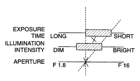
As seen in Figure 5, where the aperture size is set and the image
has a good contrast, the solution space X for determining an appropriate
contrast and illumination intensity is cone-shaped. However, if there is a
bad contrast, minimal adjustments can be made to improve the reading of
the image.
No specific algorithm for selecting an appropriate aperture size,
contrast or illumination intensity is provided herein as a number of
appropriate algorithms will be evident to one of ordinary skill in the art
and any algorithm provided would be environment-dependent. For
example, where an image is being read in a specular environment, the
algorithm would minimize the increase in illumination intensity to avoid
too large an increase in light which would interfere with the reading of the
image. As another example, if one is reading images outdoors, or indoors
near a window exposed to bright light, the algorithm would probably
modify the shutter speed before making any other adjustments.
Based on the above description, it should be understood that the
camera of the present invention may be mounted at a fixed station, or
may be a portable unit and may be hand-held and/or battery operated.
It should be further understood that the embodiments and
variations shown and described herein are illustrations only and that
various modifications may be implemented by those skilled in the art
14
CA 02253820 1998-11-03
WO 97/42756 PCT/US97/07884
without departing from the scope and spirit of the invention. For
example, although the above description refers to capturing an image with
a PSCCD sensor, image may be captured sensor which captures a full
frame of information in a non-interlaced format, such as a CMOS sensor.