Note: Descriptions are shown in the official language in which they were submitted.
CA 022~40~l l998-ll-lO
WO 97/44891 PCT/US97/08207
ELECTROSTATIC CHUCK
Background of the Invention
The present invention relates to methods and ap~ us for securing a
semiconductor substrate to a chuck, and more particularly to methods and apparatus
for electrostatically clamping a semiconductor substrate to a chuck.
In the fabrication of integrated circuits, a number of well-established
processes are used to treat and process a semiconductor wafer. Apparatus for
clamping the wafer can be used with any conventional processing technique. Theseprocesses include, for example, chemical vapor deposition, ion implantation, ionbearn milling and reactive ion etching. One example is conventional ion
implantation systems which include an ion source that ionizes a desired dopant,
which is then accelerated to form an ion beam of prescribed energy. The ion beam is
then directed at the top surface of a target wafer. The energetic ions in the beam
penetrate into the bulk of the semiconductor material and are embedded in the
crystalline lattice of the semiconductor material to form a region of desired
conductivity. This ion implantation process is typically performed in a high
vacuum, gas-tight process chamber which encases a wafer h~ndling assembly.
An important feature of conventional ion implantation systems is the
securing or clamping of the semiconductor wafer to the wafer handling assembly.
This clamping feature properly positions the wafer at a selected location while
facilitating cooling of the wafer by rigidly and tightly clamping the wafer to the
relatively cool platen surface of the wafer h~ndling assembly. Wafer cooling is
particularly important in commercial semiconductor processing where a major
objective is to achieve a high throughput implantation system in terms of wafersprocessed per unit time. One way to achieve such a high throughput system is to use
a relatively high current ion beam which implants wafers in a relatively short period
of time. The use of high current implanters, however, generate large amounts of
heat which can result in uncontrolled diffusion of impurities beyond prescribed
limits in the wafer and in degradation of patterned photoresist layers. It is thus
usually necessary to provide structure that cooperates with the clamping meçh~ni~m
to cool the wafer in order to limit the maximum wafer temperature. A variety of
techniques for clamping and cooling the wafer to the wafer h~n~lling assembly have
been developed and are known in the art.
According to one well-known technique, the wafer is clamped against
the platen surface of the wafer handling assembly by a peripheral clamping ring
CA 022~40~1 1998-ll-lO
WO 97/44891 PCT/US97/08207
which engages the outer peripheral portion of the wafer. The front surface of the
wafer is then exposed for ion implantation. A drawback of this type of clarnpingassembly is that the ring covers a portion of the outer periphery of the wafer, thus
preventing that portion from being implanted by the ion source. Another drawbackis that peripheral clamping does not result in physical contact between the wafer and
the flat metal platen over the entire wafer surface area. This occurs since the
clamping force is applied to just the peripheral edge and not uniformly across the
entire wafer surface, and thus does not pull the wafer flat against the platen surface.
One advantage of uniform clamping of the wafer to the platen is that it provides for
more efficient cooling of the wafer. In many of these conventional configurations,
however, thermal transfer is inadequate due to poor contact between the
semiconductor wafer and the platen surface.
Another drawback of conventional peripheral clamps is that
obscuring a portion of the usable wafer area reduces the overall wafer yield, thus
increasing waste and production costs. Still another drawback is that the peripheral
ring clamp creates unwanted wafer stress that may create microcracks within the
wafer. The presence of microcracks within the wafer may affect the operating
performance of the integrated circuits formed on the wafer, thus rendering unusable
portions of the wafer or indeed the entire wafer itself.
A wafer clamping technique which elimin~tes the requirement for a
peripheral cl~mping ring and which permits use of a flat platen surface is centrifugal
clamping. In centrifugal clarnping, the semiconductor wafer is rotated about an axis
of rotation by known rotation machinery. The platen surface is typically oriented at
an angle with respect to the axis of rotation so that centrifugal force presses the
wafer against the platen surface. A drawback of this system is that the rotationmachinery is relatively complex and expensive, and thus adds to the overall cost of
the system.
Another known technique for clarnping semiconductor wafers
involves the use of electrostatic chucks (ESCs). Although ESCs vary in design, they
all are based upon the same physical principles, namely, the creation of an
electrostatic force between the platen surface and the semiconductor wafer. Typical
ESCs include an electrically conductive electrode that is mounted on a pedestal and
covered by an electrically insulative, dielectric material. The semiconductor wafer
seats on top of the insulative material. A voltage source electrically biases the
electrode so that electric charge accumulates in the electrode and the insulative
material. The applied voltage then induces an equal and opposite charge on the rear
CA 022~40~1 1998-11-10
WO 97144891 PCT/US97/08207
surface of the wafer. This accumulated electric charge generates an electrostatic
force that attracts and clamps the wafer against the insulative material. The amount
of clamping charge, which determines the clamping force, is dependent, among
others, on the thickness of the dielectric material and the material's dielectric
5 constant.
An advantage of conventional ESCs is their ability to pull the wafer
substantially flat against the platen surface of the wafer h~n(lling assembly byapplying the clamping voltage/force across the entire wafer surface, and not just at
the edges. This allows for more effective and efficient cooling of the wafer, while
10 concomitantly avoiding the microcracks that can develop when using conventional
mechanical clamps, such as ring clamps, and cooling structure.
Another advantage of ESCs is that they do not employ structure that
engages the top surface of the wafer. This increases the overall wafer yield since the
entire wafer surface is available for proce~sing.
The insulative layer is typically composed of polyimides and other
organic polymers because of their resistance to high voltage breakdown and theirsuperior chemical reei.ct~nce. Further, the ability of the polyimide to conform to the
backside of the substrate allows for good heat transfer for wafer cooling duringprocessing. A drawback of polyimides and other organic polymers is that they react
20 rapidly when exposed to corrosive gases such as phosphene, oxygen, chlorine and
fluorine, which are typically used in the processing of semiconductor wafers.
A significant problem with conventional ESCs is that the dielectric
material becomes polarized over time, and tends to act as a permanent magnet,
clamping the wafer to the platen surface until long after the scheduled release time.
25 These residual electrostatic forces may arise from permanent polarization of the
dielectric material, from slow mobile ions located within the dielectric, or more
commonly from charges trapped at the dielectric surface or wafer backside when the
wafer has an in~ul~ting layer. This unwanted and prolonged clamping of the waferto the platen surface increases the wafer processing time, while concomitantly
30 introducing an element of unreliability into the wafer manufacturing process.Due to the foregoing and other shortcomings of conventional ESCs,
an object of this invention is to provide an ESC that reduces the occurrence of
unwanted wafer clamping to the platen surface.
Another object of the invention is to provide an ESC that allows for
35 relatively high efficiency cooling of the wafer.
CA 022~40~1 1998-ll-lO
WO 97/44891 PCT/US97/08207
Still another object of the invention is to provide an ESC that does
not become polarized over time.
Other general and more specific objects of the invention will in part
be obvious and will in part appear from the drawings and description which follow.
s
Summary of the Invention
The present invention attains the foregoing and other objects by
providing an electrostatic chuck according to the teachings of the present invention
and methods for producing the same. The electrostatic wafer-holding chuck of the10 invention includes first and second dielectric plates formed of single crystal
aluminum oxide and at least one electrode disposed within a recess formed in thefirst dielectric plate. The single crystal material preferably does not contain polar
molecules that are free to align in the direction of an externally applied
electromagnetic field. Specifically, the preferred single crystal material either does
15 not contain polar molecules or contains polar molecules that are restricted in
movement, such as those molecules that are bound in or form part of a single crystal
lattice structure. Consequently, the material does not become polarized over time,
and thus repeatedly and rapidly releases the wafer at the scheduled release time.
The electrostatic chuck of the present invention forrns a substantially
20 monolithic, hermetically sealed chuck when the first and second dielectric plates are
diffusively jointed together.
According to one aspect of the invention, the second dielectric plate
has a top wafer-supporting surface that has a fluid distribution network formed
therein. The distribution network channels a heat transfer fluid to the backside of the
25 wafer. According to a preferred practice, the fluid distribution network formed in
the second dielectric plate includes a gas distributor and a plurality of radially
outwardly extentling gas passages that are in fluid communication with the gas
distributor. The distribution network can further include a radially outer annular gas
passage that surrounds and communicates with the gas distributor and the outwardly
30 extl?n~ling gas passages.
According to another aspect, when the first and second dielectric
plates are assembled, the first dielectric plate is disposed contiguous to the second
dielectric plate such that a bottom surface of the second dielectric plate intimately
contacts at least a peripheral top portion of a top surface of the first dielectric plate.
35 According to one practice, the first and second plates are diffusively joined together
to form a monolithic, hermetically-sealed electrostatic chuck.
~
CA 022~40~1 1998-ll-lO
WO 97/44891 PCT/US97/08207
According to another aspect, the single crystal dielectric plates each
have a C-axis that are aligned so that they are generally parallel relative to each
other, and form an angle therebetween of between about 1 degree and about 5
degrees, and preferably less than about 1 degree, when the electrostatic chuck is
constructed.
According to another aspect, the first dielectric plate includes a first
fluid manifold and an electrical passage that extend between the top and bottom
surfaces and the second dielectric plate includes a second fluid manifold. According
to one practice, the first and second fluid manifolds align to form a central fluid
manifold when the two plates are assembled.
The present invention further includes a method for producing a
hermetically sealed electrostatic chuck that includes the steps of (1) providing a first
dielectric plate formed of a single crystal material having a recess formed therein, (2)
providing a second dielectric plate formed of a single cr~ystal material having a
plurality of gas channels formed therein, (3) placing the second dielectric plate
contiguous with the first dielectric plate, (4) heating said first and second dielectric
plates to an elevated tt;l,lp~ldl-lre in the range of about 1900~ C and about 2050~ C to
diffusively join the first and second dielectric plates together.
According to one aspect, the method further includes the step of
disposing an electrode in the recess of the first dielectric plate.
Other general and more specific objects of the invention will in part
be obvious and will in part be evident from the drawings and description which
follow.
Brief Description of the D~
The foregoing and other objects, features and advantages of the
invention will be ~CIIl from the following description and appalcn~l from the
accompanying drawing, in which like reference characters refer to the same partsthroughout the different views. The drawing illustrates principles of the invention
and, although not to scale, show relative dimensions.
FIG. 1 is a cross-sectional view of the electrostatic chuck of the
present invention.
FIG. 2 is a top view of the bottom single crystal dielectric plate of
FIG. 1.
FIG. 3 is a top view of the top single crystal dielectric plate of FIG. 1
showing the gas distribution network of the electrostatic chuck.
CA 022~40~1 1998-11-10
WO 97/44891 PCT/USg7/08207
Description of Illustrated Embodiments
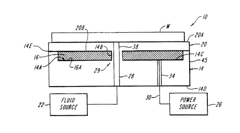
FIGS. 1-3 show the electrostatic chuck 10 of the present invention.
The illustrated electrostatic chuck includes a bottom dielectric plate 14, a top5 dielectric plate 20, an electrode 16 which is preferably disposed between the top and
bottom plates 14, 20, and a workpiece W. The workpiece preferably seats on top of
the top dielectric plate 20 or other portion of the chuck. A gas source 22 is coupled
to a central fluid manifold 29 formed by fluid passageways 28, 38 of the top andbottom dielectric plates l 4, 20. A power source 26 is coupled to the electrode 16
l 0 through an appropriate electrical lead 30. The workpiece W is typically the
precursor of an integrated circuit, a flat panel liquid crystal display, or a wafer which
has been positioned and disposed for proces~ing by known processing techniques,
such as ion implantation or chemical vapor deposition. The illustrated electrostatic
chuck 10 is typically employed to either transport the workpiece W into and out of a
15 processing chamber, such as the process chamber of an ion implantation system, or
serves to electrostatically clamp the workpiece W during processing. The
electrostatic chuck l 0 further employs thermal control structure to help cool the
workpiece before, during or after procec~ing, as is described in further detail below.
The illustrated electrostatic chuck l 0 provides a simple and elegant
20 solution that overcomes problems typically associated with conventional
electrostatic chucks. One common problem with conventional chucks is the
difficulty of removing the electric charge from the workpiece W and the chuck
assembly, e.g., the insulative (dielectric) material, when it is desired to release the
workpiece from the chuck, such as upon completion of proces.cing. Another
25 common problem with these ESCs is that the dielectric material becomes polarized
over time and tends to act much like a perm~n~nt "magnet" (actually an electret),
thus clamping the workpiece W to the chuck assembly long after the scheduled
released time. These residual forces which remain in the electrostatic chuck even
after the cessation of power can arise from permanent polarization of the dielectric,
30 from slow mobile ions located inside the dielectric material, or more commonly
from charges trapped at the dielectric circuits or wafer backside, when the wafer has
an in.~ ting layer. The uncertainty which is introduced to the m~nl-f~cturing
process by the unwanted continuous clamping of the workpiece to the electrostatic
chuck creates problems in implantation systems, and particularly in high throughput
35 ion implantation system. The electrostatic chuck of the present invention addresses
these concerns by providing for an electrostatic chuck that does not become
CA 022~40~1 1998-ll-lO
WO 97/44891 PCTIUS97/08207
polarized over time. According to a preferred practice, the electrostatic chuck of the
invention overcomes this problem by ~ltili7ing a pair of dielectric plates that are
formed of a high purity, single crystal dielectric material so as to form a substrate
with polar molecules that are bound in or forrn part of a substantially unidirectional
crystalline lattice, as described in further detail below.
Referring to FIG. 1, the electrostatic chuck 10 includes a bottom
dielectric plate 14 that has a recess 14A that seats the electrode 16. The recess 14A
preferably includes a central hub portion 14B that extends upwardly from a floor14C ofthe recess 14A. The hub portion 14B is configured, in one embodiment, to
seat in a central punch hole formed in the interior portion of the electrode 16.The illustrated bottom dielectric plate 14 further includes a fluid
passageway 28 that extends between the bottom surface 14D and the top surface 14E
of the plate, and an electrical port 34 that opens at one end onto the floor 14C of the
recess 14A. The illustrated electrical port forrns a through passage that allows a
corresponding electrical lead, e.g., electrical lead 30, to contact the rear surface 16A
of the electrode 16.
The top dielectric plate 20 is preferably disposed adjacent to and
coextensively with the bottom dielectric plate 14. The dielectric plate 20 includes a
central fluid passageway 38 that aligns with the fluid passageway 28, when the two
dielectric plates are mounted together, to form a single central fluid manifold 29. A
top surface 20A of the dielectric plate 20 has a fluid distribution network 40 formed
therein. The illustrated distribution network 40 includes a central fluid hub 42 that is
in fluid communication with a plurality of radially outwardly extending ch~nnt l~ 44
that termin~te in a circumferentially located, annular fluid channel 46.
The illustrated diskibution network 40 provides for efficient and
uniform cooling or heating of the workpiece W. The central fluid hub 42 functions
as a fluid distributor by distributing a heat transfer fluid from the central fluid
manifold 29 to each individual radially outwardly extending fluid channel 44. The
network 40 thus distributes a heat transfer fluid, such as helium, argon or any
suitable liquid, about selected portions of the backside of the workpiece W to
provide effective heat transfer between the wafer and the electrostatic chuck 10.
The illustrated fluid distribution network 40 has a selected ratio of
channel spacing to channel width that is sufficiently large to distribute the heat
transfer medium about the backside of the workpiece W while concomitantly being
relatively small so as not to occupy a significant fraction of the surface area of the
top surface 20A of the dielectric plate 20. The illustrated fluid channels 44 are
-
CA 022~40~1 1998-ll-lO
WO 97/44891 PCT/US97/08207
- 8 -
selected so as to maximize the heat transfer capabilities between the heat transfer
fluid and the worl~piece W. These fluid channels can be formed by known
machining techniques, including laser machining and abrasive machining, such as
ultrasonic abrasive machining.
S The particular pattern and arrangement of the fluid ch~nnel~ 44 andthe particular number and sizes of the channels can be selected or deterrnined by the
ordinarily skilled artisan to maximize the heat transfer between the heat transfer
fluid/chuck and the wafer W. The particular arrangement of the components of thefluid distribution networlc 40, such as the fluid channels 44, can vary depending
10 upon such factors as the size of the dielectric plates, the size of the wafer, the desired
maximum wafer temperature, the type of heat transfer medium, and the wafer
processing environment. One of ordinary skill in the art would be able to study the
aforementioned factors, as well as other factors known to those in the art, to
determine the ~plo,t,liate configuration of the fluid distribution network, without
15 undue experimentation. According to a l,le~lled embodiment, when utili7ing top
and bottom dielectric plates having a diarneter of about 155 mm, the number of
radially extending fluid channels 44 can range between about 6 and about 10. Those
of ordinary skill will appreciate that other configurations can be employed to effect
cooling of the wafer W. The channels preferably have a width between about 1.5
20 mm and about 4 mm, and most preferably about 2 mm, and have a depth between
about 0.04 mm and about 0.10 mm, and most preferably about 0.05 mm deep.
The top dielectric plate 20 preferably has a thickness of about 0.25
mm and the bottom dielectric plate preferably has a thickness ranging between about
2.5 mm and about 6.0 mm. The annular recess 14A forrned in the bottom dielectric25 plate 14 is approximately 0.025 mm deep. The shoulder portion 15 of the bottom
dielectric plate 14 preferably has a thickness ranging between about 1 mm and about
2 mm. The top plate is preferably relatively thin to allow a suitable electrostatic
force to develop between the wafer W and the top dielectric plate 20. The bottomdielectric plate 14 is preferably relatively thick to provide mechanical support for the
30 workpiece W and seats electrode 16 that is preferably about 0.20 mm thick.
The raised top portion 14E of the bottom dielectric plate 14, which
includes the raised peripheral shoulder portion 15 and the central hub 1 4B, and the
rear surface 20B of the top dielectric plate 20 are preferably polished to a flat and
smooth surface by conventional polishing techniques.
The present invention overcomes the unwanted and inconsistent
clamping problems associated with conventional electrostatic chucks by forming the
.. . . .
CA 022~40~1 1998-ll-lO
WO 97/44891 PCTIUS97/08207
top and bottom dielectric plates 14, 20 of a single crystal dielectric material. The
single crystal dielectric material preferably does not contain polar molecules that are
free to align in the direction of an externally applied electromagnetic field. Hence,
the preferred single crystal dielectric material either does not contain polar
S molecules or contains polar molecules that are restricted in movement, such as those
molecules that are bound in a single crystal lattice structure. The l"efelled dielectric
material also has a relatively high breakdown field strength, i.e., the material can
with.~t~ntl relatively high voltages without breaking down internally. The material
also preferably can be used in high tempeldL~lre operating environments and thus10 exhibits good dielectric properties at elevated temperatures. The single crystal
dielectric material can include diamond, boron nitride, quartz and m~gn~cium oxide,
and preferably is aluminum oxide (Al2O3)
The single crystal alnminllm oxide of the present invention can be
formed by conventional manufacturing processes, such as those described in U.S.
Patent No. 3,591,348 of LaBelle, Jr., U.S. Patent No. 3,687,633 of LaBelle, Jr. et al.,
U.S. Patent No. 3,826,625 of Bailey, and U.S. Patent No. 3,953,174 of LaBelle, Jr.,
the te~ching.s of which are hereby incorporated by reference.
The top and bottom dielectric plates 14, 20 are preferably made of a
single crystal dielectric material each having a selected crystallographic orientation
20 that are nearly parallel to each other. More specifically, the crystallographic
orientation of the material comprising each plate 14, 20 are transverse relative to
each other and form a relatively small angle therebetween, e.g., are essentiallyparallel. By way of example, the single crystal dielectric material can comprise an
A-plane material which includes a surface norrnal that lies in the <1120>
25 crystallographic direction. This material further includes a C-axis which lies in the <
0001 > direction, and which typically lies within and is parallel to the plane of the
plate. The C-axes of the top and bottom dielectric plates 14, 20 are preferably
transverse relative to each other and form an angle therebetween of less than about 5
degrees, and more preferably less than about 1 degree. This preferred orientation of
30 the C-axes reduces the occurrence of fracturing of the bond between the top and
bottom plates when bonded together when the plates are cooled from the elevated
bonding lem~ re to a suitable h~ntlling temperature, e.g., room t~ p~ e.
The electrostatic chuck 10 of the present invention is assembled as
follows. The top and bottom dielectric plates 20, 14 are made from a single crystal
35 dielectric material according to known techniques, and machined to have the
a~p~upliate size electrode recess and fluid and electrical conduits. The top dielectric
CA 022~40~1 1998-ll-lO
WO 97/44891 PCT/US97/08207
- 10-
plate 20 is further machined by known methods to include the fluid distribution
network 40. The electrode 16 is formed to have a selected size and is placed within
the recess 14A. The top dielectric plate 20 is then placed on top of the bottom
dielectric plate and the fluid passages 28, 38 are aligned to form the central fluid
5 manifold 29. The electrostatic chuck 10 is then formed into a hermetically sealed
structure by heating the axially successive assemblage of the top and bottom
dielectric plates 20, 14 and electrode under high vacuum at an elevated temperature
between about 1900~C and about 2000~C, and most preferably between about
1900~C and 1950~C, while concomitantly applying a pressure to place the polishedbottom surface 20B of the top plate 20 in intimate facing contact with the top surface
14E of the bottom plate 14.
The high t~ c~ re heating of the electrostatic chuck assemblage
promotes interdiffusion of the surfaces of the top and bottom plate to produce ahermetic seal between these components parts that possess the full dielectric strength
of the single crystal dielectric m~teri~l. Because of the high temperature
requirements for the diffusive joining of the plates of the electrostatic chuck 10, the
electrode 16 is preferably made from an electrically conductive material having a
relatively high melting point, or a melting point above the diffusion bonding
temperature of the single crystal dielectric material, e.g., above about 1900~C.Suitable metals include the refractory metals. The electrode 16 preferably has athickness ranging between about 0.10 mm and about 0.20 mm.
The power source 26 is disposed in electrical con~llw-ication with the
sealed electrode 16 by welding an electrical lead to the back surface of the electrode
16, which in turn is connected to an ~plol,.;ate pole of the power source. A fluid
source 22 which contains a supply of a heat transfer fluid l is disposed in fluid
communication with the fluid manifold 29 formed by the aligned fluid passageways28, 38 via suitable fluid conduits. The fluid conduits preferably comprise a metal
tube that is brazed onto the bottom surface 14D of the bottom dielectric plate 14.
The tube preferably is composed of a metal alloy having a thermal expansion
coefficient that is closely m~t~he~l to that of the single crystal dielectric material,
e.g., al--minl-m oxide. This metal tube can then be brazed to a tube formed of ahigher expansion material, such as stainless steel, to afford a hermetic and
mechanically reliable fluid connection ~etween the fluid source 22 and the illustrated
electrostatic chuck 10.
In operation, a workpiece W is place on the top surface 20A of the
top dielectric plate 20. An electrostatic charge is generated by the application of a
CA 022~40s 1 1998 - l l - lO
WO 97/44891 PCT/US97/08207
voltage, supplied by power source 26, to the electrode 16 along electrical lead 30.
The applied voltage produces an equal and opposite charge on the rear surface of the
wafer, thus electrostatically clamping the wafer to the top surface 20A of the
dielectric plate 20. The particular amount of charge, which determines the
5 magnitude of the clamping force, is dependent upon the thickness of the dielectric
material, the dielectric material's dielectric constant, the spacing of the vacuum gap
between the wafer and the dielectric, and the clamp voltage. The wafer is then
processed according to known processing techniques. By way of example, during
these processing techniques, the wafer W can be heated to a selected elevated
10 temperature. Ideally, semiconductor wafers are m~int~ine~l at temperatures below
1 00~C to prevent damage to the photoresist typically formed on the semiconductor
wafer W. To control the t~lllpc.dlul~ of the semiconductor wafer, a selected heat
transfer fluid, such as helium, is supplied by the fluid source 22 and coupled to the
aligned fluid passageways 28, 38 by the foregoing fluid conduits. The applied fluid
15 is distributed by the hub gas distributor 42 to the radially outwardly extending fluid
passages 44. The heat transfer fluid convectively transfers heat from the wafer W to
the electrostatic chuck and the cooling fluid. The fluid is then transported to the
circurnferential passage 46 and is removed therefrom by appl~,.;ate exhaust
structure. The heat transfer that occurs between the wafer and fluid, and between the
20 wafer and electrostatic chuck surface helps m~int~in the teyeldlul e of the
semiconductor wafer W below critical telnp~"dlures.
Once processing is complete the power source 26 is turned off to
cessate the application of power to the electrode 16. This subst~nti~11y
instantaneously releases the semiconductor wafer W from the electrostatic chuck 20.
Hence, the electrostatic chuck l 0 of the invention easily releases the wafer W at the
scheduled release time. Alternatively, the semiconductor wafer W can be
disengaged from the electrostatic chuck l 0 by the application of a de-ch1-rl~ing
voltage which has a magnitude similar to the voltage applied during proces~ing, but
of opposite polarity.
The electrostatic chuck l 0 illustrated in FIG. l can be of a monopolar
or bipolar design. In the illustrated monopolar design, the electrostatic chuck l 0 is
typically employed only during the ion implantation process, since the applied ion
plasma stream serves to discharge the energy applied by the power source 26 to the
electrode, and which accumulates at the wafer surface. Conversely, the illustrated
electrode l 6 can be formed from two separate and electrically isolated electrodes,
formed as semicircular electrodes, to form a bipolar design. In this design, the first
CA 022~40~1 1998-ll-lO
WO 97/44891 PCT/US97/08207
electrode is coupled to the positive pole of the power source 26 and the other
electrode is connectecl to the negative pole of the power source. This electrical
configuration m~int~inc the electrode at a ground potential. Hence, the bipolar
design can be used before or after the implantation process.
The power source 26 can be either an AC or a DC power source
depending upon the particular processing environment. Thus, for example, in the
case of low throughput etch and plasma deposition systems, a DC clamping voltageis typically used to electrostatically clamp the semiconductor wafer W to the
electrostatic chuck 10. In high throughput ion implantation systems, a bipolar
polyphase AC power source is used to generate the electrostatic charge which
electrostatically clamps the semiconductor wafer W.
A significant advantage of the present invention is that the
electrostatic chuck of the invention which is composed of a single crystal dielectric
material releases the semiconductor wafer substantially at the scheduled releasetime. The single crystal dielectric material, such as aluminum oxide, provides for
this rapid-release action since the free molecules (if present) of the dielectric
material cannot align with the applied electric field.
It will thus be seen that the invention efficiently attains the objects set
forth above, among those made al,palellL from the preceding description. Since
certain changes may be made in the above constructions without departing from the
scope of the invention, it is intended that all matter contained in the above
description or shown in the accompanying drawings be interpreted as illustrative and
not in a limiting sense.
It is also to be understood that the following claims are to cover all
generic and specific features of the invention described herein, and all statements of
the scope of the invention which, as a matter of language, might be said to fall there
between.
Having described the invention, what is claimed as new and desired
to be secured by Letters Patent is: