Note: Descriptions are shown in the official language in which they were submitted.
CA 022~4213 1998-12-09
Optical receiver for receiving digitally transmitted data
The invention is derived from an optical receiver for
receiving digitally transmitted data as per the species of
the main claim.
When digital signals with a high bit sequence frequency
(gigabit range) are transmitted, various dispersion effects
occur caused by optical fibre cables in the optical
transmission system. These dispersion effects distort the
data signals, thus limiting the transmission lengths.
Distortions can also occur on the optical fibre due to non-
linear effects, e.g. the Kerr effect. optical receivers used
in such a transmission system are required to evaluate
distorted signals, permitting only low bit error rates. It is
known from the publication "Decision-point steering in
optical fibre communication system", M. Sherif, IEEE
Proceedings, Volume 136, No. 3, 1989, page 169 ff, that a
receiver in a digital optical transmission system can be
optimized by modifying decider thresholds, thus generating
artificial errors. For this purpose a second decider circuit
is applied parallel to the main data flow. This second signal
branch is subjected to a large number of bit errors. The
artificial error rate is achieved in the publication in
question by modifying the decider threshold, which is changed
by means of a square pulse. The results of the two deciders
are compared, and from the result actuating variables are
derived for an amplifier and for the receiving photodiodes.
If you examine the eye diagram of the signal received, the
first decider scans the eye aperture at an almost optimal
point, i.e. both the decider threshold and the scanning
window are roughly in the center of the open eye. The second
signal path changes the decider threshold so that the
threshold can already be in the noise of the eye diagram, and
so artificial errors occur. By evaluating these artificial
errors the whole optical receiver is readjusted to optimize
the eye aperture, noise characteristics, etc.
CA 022~4213 1998-12-09
A digital optical message transmission system is disclosed in
EP 0554 736 B1 in which the receiver quality is optimized by
evaluating the eye diagram. In this case an eye diagram is
recorded in the receiver, and the size of the eye aperture is
determined in a computer. The computer determines an optimum
setting of the photodiode and the decider threshold from the
data recorded. Recording an eye diagram, comparing with a
stored nominal value, and adjusting various receiver
activating variables does not enable the bit error rate to be
directly determined and a required resultant optimization of
the receiver.
The optical receiver disclosed for receiving digitally
transmitted data with the characteristic features of the main
claim has in contrast the advantage that bit error rates can
be determined, even individual bit errors being detected. The
optical receiver offers the advantage of having a pseudo-
error monitor circuit for detecting bit errors as a function
of threshold value and phase position, these measured data
serving to adjust the parameters of the filter and the
decider circuit itself. The computing unit linked to the
receiver adjusts the parameters on the basis of the measured
bit error data. The measures listed in the sub-claims enable
advantageous developments and improvements of the optical
receiver presented in the main claim. It is particularly
advantageous that in the circuit disclosed two independent
error signals are determined, the first error signal serving
to derive high bit error rates, and the second error signal
being used to detect individual bit errors.
The system has the advantage that both the phase position and
the threshold value of the decider circuits are affected. In
this case the adjustment is simply made by means of computing
unit signals using phase shifters and phase adjusting
members. In order to avoid errors of measurement through the
different phase positions, the phase position is
advantageously corrected by an additional scanning device. As
CA 022~4213 1998-12-09
a result the signal branches are scanned at the same times,
and the results are comparable.
The optical receiver in the device disclosed enables scanning
of multi-level signals to be simply compared by several
deciders being connected in parallel, and their result read
out via a switch activated by the computing unit. For reading
out multi-level signals it is important that the phase
adjustments of the various deciders are also connected to the
decider via a switch, so that any phase shift present is
avoided at readout time. The data derived offers the
advantage of acting to optimize a filter that is constructed
from a chain of input amplifiers and output amplifiers to
achieve high data rates. This makes it easy to implement a
filter function of a transversal filter even at high data
rates. In this case the digital multiplier units of the
filter are adapted by the computing unit. The filter of the
optical receiver in the device disclosed can be cascaded over
the outlets, creating a sequence of filters with which
[filters] of even higher order can be realized.
It is particularly advantageous that the amplification
factors and the weighting factors of the multiplier circuits
are variable and adjustable.
It is thus possible to optimize the filter on the basis of
data determined in the receiver.
The rope-ladder structure makes it easy to realize a filter
function of a transversal filter even at high data rates. In
this case the weighting factors of the filter's digital
multiplier unit are adapted by a computing unit. The filter
of the optical receiver in the device disclosed can be
cascaded through the outputs to create a sequence of filters
with which filters of even higher order can be realized.
Embodiments of the invention are shown in the drawings and
explained in greater detail in the following description.
Figure 1 shows the structure of an optical receiver
CA 022~4213 1998-12-09
Figure 2 a decider circuit with the optical receiver's
pseudo-error monitor
Figure 3 EXOR gate with pre-scanning
Figure 4 decider circuit for multi-level signals
Figure 5 transversal filter
Figure 6 cascaded filter configuration and
Figure 7 an example of a DST signal transmission function
Figure 8 the structure of a filter
Figure 1 shows an input signal 1 that passes first through a
filter 2 and then a decider/pseudo-error monitor circuit 3.
From the filtered signal 1', the clock contact 15 branches
off whose timing signal inputs to the decider circuit 3. A
computing unit 5 is connected to the decider circuit and to
filter 2. The computing unit 5 supplies signals, a level
adjustment 6, phase adjustments PhM, Ph, Phl, threshold value
adjustments 8, an error reset 10 to the decider circuit, and
an adjustment signal 11 to the digital filter 2. The decider
circuit 3 supplies the error signals 9 to the computing unit
5.
The incoming signals 1 are first filtered in filter 2, and
scanned in the decider circuit 3. For scanning, first the
clock pulse 16 has to be extracted from the filtered signal
1'. In the decider circuit, that has a pseudo-error monitor
circuit in the device disclosed, the input signal 1' is
scanned and the output signal 4 emitted for further
processing. The whole control of the receiver in the device
disclosed is carried out in the computing unit 5, from which
parameters 6, PhM, Phl, 8 and 10 are adjusted for the
decider/pseudo-error monitor circuit 3. The computing unit 5
also controls the coefficients of the filter 2 by means of
the filter adjustments 11. Activation from the computing unit
is effected by means of digital-to-analog converters, and the
error signal 9 is evaluated by means of an analog-to-digital
converter. Control through the computing unit is in a slow
time-frame. In this case the control system does not work
with the high incoming data rates. Conventional computing
CA 022~4213 1998-12-09
units can therefore be used for the control system. Using a
control unit also offers the advantage that the initial
values can easily be adapted both in the decider circuit 3
and also in the filter 2 by adapting the software.
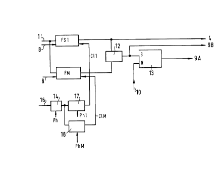
Figure 2 shows an initial variant of the decider/pseudo-error
monitor circuit 3 in the device disclosed. The filtered input
signal 1' is linked to the input of a decider FSl and a
decider FM. The outputs of the two deciders are high at the
input of an EXOR circuit. The output of the EXOR circuit 12
is linked to the input of an RS flip-flop 13 and to the data
line 9B. The R input of the RS flip-flop 13 is connected to
the reset output 10 of the computing unit. The output of the
flip-flop 13 is connected to the line 9A to the computing
unit. To adjust the decider FM, it is connected both to the
threshold value adjustment 8 and also through a phase shifter
14 and a phase adjustment 17. The decider FS1 also has a
connection to the threshold value adjustment 8, and a link to
a variable phase adjustment 18 that branches off after the
phase shifter 14. The variable phase adjustments 14, 17 and
18 are activated by phase adjustment signals Ph, Phl, PhM.
The filtered input signal 1' similarly accesses the inputs of
both the deciders FM and FS1. This involves two D flip-flops.
Both the flip-flops FM and FS1 change to state 1 on the
output side if the incoming signal 1' exceeds the threshold
values 8 at the point in time of a clock pulse edge of the
timing signals CI1 and CIM. The outputs of the flip-flops are
linked to the EXOR circuit 12 that gives a signal when there
are different signals present on the input side. The EXOR
circuit 12 gives the error signal 9B that leads to a DC
signal at high error rates by means of the integrating
characteristic of the analog-to-digital converter of the
computer. A high DC level of signal 9B thus detects a high
bit error rate. The output signal of the EXOR circuit 12 is
high at the S input of the RS flip-flop 13. The RS flip-flop
13 changes to state 1 when a 1 is high at its S input. The
flip-flop 13 can be reset via the R input. It is possible to
CA 022~4213 1998-12-09
detect individual bit errors via this RS flip-flop 13. The
flip-flop stores the individual error until the computer
analyses the output signal 9A of the flip-flop, and resets
via the input R. This enables a computing unit to read out
individual bit errors and analyze them, although the
computing unit itself cannot follow the fast data rate of the
optical transmission system. The values scanned in the
decider circuits FM and FSl are highly dependent on the
threshold values 8, and also on the scanning phase. The
decider FSl is initially operated with a fixed phase
adjustment. The timing signal 16 derived from the input
signal is input to a phase shifter 14 that activates a phase
adjustment 17. This phase adjustment is determined by the
scanning phase CIl of the decider FSl. Branching off after
the phase shifter 14, a variable phase shifter 18 is used to
determine the phase position of the second decider FM. The
phase position CIM of the decider FM can be variably adjusted
from 0-360~, in which case the adjustment is made by means of
the phase adjustment signal PhM, Ph, Phl of the computing
unit. To determine the bit error rate, the values for the
decider FSl are preset almost optimally, i.e. so that the
scanning window and the scanning threshold is roughly in the
center of the eye aperture of the signal received. By
changing the scanning threshold in the decider FM, and the
phase position CIM, the eye aperture is scanned both
horizontally and vertically. the bit error rates thus
determined serve to optimize the eye aperture and also to
optimize the decider threshold and phase of FSl, and thus the
reception characteristics of the optical receiver.
Figure 3 shows an alternative circuit of the EXOR gate 12, an
expansion being made by means of two further deciders FSE and
FME. The circuit described in Figure 2 can lead to problems
since the two scanning results to be compared of the two
deciders FSl and FM are not scanned at the same time. By
inserting a second decider FSE and FME in the two signal
branches that are activated respectively by the CIM phase of
CA 022~4213 1998-12-09
.
the decider FM, it is possible to exclude a source of error
by after-scanning at the same point in time. The 12* circuit
for example replaces the EXOR gate 12 in the variants in Fig.
2 and Fig. 4.
Figure 4 shows the decider/pseudo-error monitor circuit with
an expansion for multi-step signals. For example an optical
signal for transmitting multi-step signals is disclosed in
the patent application open to public inspection DE 43 41
408. In this case high data rates are achieved by adding
several electrical digital signals, the bit sequences being
transmitted optically as multi-step signals. In the optical
receiver there is then a decider circuit that retrieves the
digital signals. Figure 4 shows such a decider/ pseudo-error
monitor circuit. The incoming data signal 1 is split to
deciders FM to FSN connected in parallel. The deciders FM to
FSN are each adjusted with optimal threshold values 8 and
optimum scanning phases CIM to CIn. The bit error rate is
determined via the decider FSl only with a fixed-adjustment
decider FM to FSN. Which decider is compared with the values
of the decider FSl in the EXOR circuit 12 is set by means of
a switch 19. The switch 19 connects the output of one of the
deciders connected in parallel to an input of the EXOR
circuit 12. The switch 19 is activated by means of the level
adjustment 6 of the computing unit. If for example a four-
level signal is received, three deciders FM to FSN are
necessary. Each of the three deciders is optimally adjusted
both in terms of its threshold value and of its phase
position. The error detection scans only one eye for the
respective decider, as selected by the computer. The bit
error rate for the eyes of the multi-level signal are not all
determined at the same time. Even with the circuit shown in
Figure 4, the problem arises that avoidable errors occur by
scanning at different phase positions. Therefore it is an
advantageous expansion to use circuit 12* with the additional
pre-scanning of the signal in this case as well.
CA 022~4213 1998-12-09
A sample variant of filter 2 is shown in Figure 5. The input
signal 1 is passed through a chain of input amplifiers 22.
After each input amplifier 22 the signal is diverted to
multipliers 23 that are each connected on the output side to
the output amplifier chain 25. The multipliers 23 are
activated by the filter adjustment signals 11. The
multipliers 23 each have their own multiplication factors.
Input signal 1 is subject to a delay time ~ in each amplifier
cell 22 and 25. The input signal is displaced in time by
means of the amplifier cells, which have for example an
amplification factor of 1, and by weighting the multipliers,
reassembled to a filtered signal 1'. A symmetrical filter
structure of this type has the advantage that no summation is
required of all signals at one common point, which creates
problems at high data rates. The proposed symmetrical filter
structure also works reliably at high data rates. Such a
transversal filter as per Figure 5 corresponds for example to
a low-pass filter depending on the adjustment of the
coefficients. It is discernible from Figure 6 that the
transversal filter 2 can be simply concatenated with
additional identical filters. The filter has connections
through outputs 24 that can serve directly to link the next
filter block. By cascading several filter blocks 2 it is
possible to create filters of even higher order. A sample
application of an optical receiver with a transversal filter
as well as a pseudo-error monitor is shown in Figure 7. This
involves the transmission function a of a DST signal.
Transmitting a DST signal is described in greater detail in
EP 0 554 736. The transmission function of a DST signal shows
a high-pass characteristic curve. For optimum detection of
the signal, low-pass filtering of the signal a is desirable.
Simple low-pass filtering, as also described in EP 0 554 736,
produces a result that is represented by the graph b. A
transversal digital filter as per Figure 6, a higher order
cascaded version of which is shown in Figure 7, can
significantly improve the result. The transmission function c
shows an idealized picture of the use of a digital filter.
CA 022~4213 1998-12-09
The use of the optical receiver disclosed for receiving DST
signals thus has beneficial effects on bit error rates and
sensitivity of the optical receiver. In this case both the
filter characteristic curve of the digital filter and the
decider adaptation both have an optimizing effect on the
whole reception system by determining the bit error rate. The
optical receiver disclosed also serves to detect signals that
for example are received with interference because of
polarization mode dispersion. Its use is thus not limited to
DST signals or multi-level signals.
A sample variant of the filter is shown in Figure 8. The
input signal 1 passes through a chain of input amplifiers 22.
After each input amplifier 22, the signal is diverted to a
multiplier 23 that are each connected to the output amplifier
chain 25 on the output side. The multipliers 23 are activated
by the filter adjustment signals 11. The multipliers 23 each
have their own weighting factors. The input signal 1 is
subject to a delay time _~1 or _~2 at each amplification cell
22 and 25. The input signal is displaced in time through the
amplifier cells that for example have an amplification factor
of 1, and reassembled to form a filtered signal through the
weighting of the multipliers. Such a symmetrical filter
structure has the advantage that the signals do not all have
to -be summated at a common point, which is problematic at
high data rates. The proposed symmetrical filter structure
also works reliably at high data rates. A transversal filter
of the type shown in Figure 8 corresponds for example to a
low-pass filter depending on the adjustment of the
coefficients. It can be seen from Figure 8 that the
transversal filter can easily be concatenated with additional
identical filters. Through the outputs 24, the filter has
connections that can serve directly to link the next filter
block. By cascading several filter blocks, it is possible to
realize filters of even higher order.