Note: Descriptions are shown in the official language in which they were submitted.
~ - CA 02254389 1998-11-17
~ . !
577-203 CIP
(AE 454 CP)
IMPROV~,n COVER FOR AN EDGE MOUNTED
PRINTED CIRCUIT BOAR~ CONNECTOR
S CROSS R~.FER~NCE TO RELATED APPLICATION:
This application is a continuation-in-part of U.S. Application Serial No.
08/741,011, filed October 31, 1996, entitled "COVER FOR AN EDGE MOUNTED
PRINTED CIRCUIT BOARD CONNECTOR".
FIELD OF THE INVENTION:
The present invention relates generally to an electrical connection assembly
adapted for establishing electrical and mechanical engagement to a printed circuit board.
More particularly, the present invention relates to a removable cover and an edge
mounted printed circuit board connector which permits the secure positioning of the
connector to the edge of the printed circuit board so as to permit solder connection of the
connector to the printed circuit board.
BACKGROUND OF THE INVENTION:
There are a wide variety of electrical connectors which are adapted to be mated
with a printed circuit board. Many of these connectors, referred to as header connectors,
are supported adjacent an edge of the printed circuit board so as to be accessible for
external electrical connection with a mating connector.
.... ....
- CA 022~4389 1998-11-17 .'
These header connectors typically include an insulative housing which supports aplurality of electrical contacts therein. The contacts include tail portions which extend
from the housing and are adapted for electrical engagement with electrical traces on the
printed circuit board. The solder tails çxtPnt1ing from the housing of the header connector
S are aligned with solder pads of the traces of the printed circuit board so that the solder
tails may be ultimately soldered to the solder pads effecting p~rm~n.?nt mechanical and
electrical engagement b~lw~ell the header connector and the printed circuit board. The
- solder tails are typically spring biased so as to exert a spring force against the solder pads
of the printed circuit board so that effective electrical engagement is established and
m~int~ine(l upon placement of the header connector on the edge of the printed circuit
board.
As these header connectors are mounted to an edge of the printed circuit board,
the connectors may be subject to tilting or movement during the m~nllf~cturing process
prior to solder connection of the tails to the pads. Tilting or movement of the connector
with respect to the printed circuit board may cause a dislodgement of one or more of the
solder tails from the solder pad. Furthermore, warpage of the printed circuit board is
often found. Such warpage may result in intermittent contact between the solder pads.
Additionally, as the solder tails are typically spring biased to assure engagement with the
solder pads, excessive titling, warping or movement may result in loss of resiliency of the
spring biased tails.
.. . . .. . .
' - CA 022~4389 1998-11-17
One technique to overcome such problems is to rigidly clamp the header
connector to the printed circuit board prior to soldering so as to prevent movement of the
connector with respect to the board. Clamping of the connector to the board often
requires use of fastening hardware such as screws which are mounted through the
connector and into holes located in the printed circuit board. Use of such securement
hardware may hlte.rele with the soldering process rendering such soldering difficult and
costly. Furthermore, rigidly clamping the connector to the printed circuit board also
results in other problems. For instance, m~rhAnical fAct~nin~ in this marmer may also
result in the spring bias of the solder tails losing their resiliency and thereby losing
effective electrical engagement with the solder pads of the traces.
In order to alleviate certain of these problems it has been found that an edge
mounted header connector may be formed with one or more gripper arms which extend
from the insulative housing and underlie the solder tails at one or more locations along
the length of the header connector. The gripper arrns and the solder tails form a space
therebetween which accommodates the edge of the printed circuit board. To a great
extent the location of the gripper arms prevents the adverse effects of connector tilting
with respect to the printed circuit. Thus the solder tails are maintained in contact with the
solder pads during and after the soldering process. A connector having such gripper
arrns and exhibiting such advantages is shown and described in commonly assigned U.S.
patent application entitled " SINGLE-SIDED STRADDLE MOUNT PRINTED
CIRCUIT BOARD CONNECTOR", filed October 23, 1996, bearing attorney docket
, ._, . . . . . , . ~.. ~_ _
- . CA 022~4389 1998-11-17
,
number 577-155. While the structure shown and described in that application serves
adequately for its int~n~ed function, the connector itself must be formed to have such
gripper arms. This requires forming a specialized connçctor having the gripper arm
feature formed therewith. In certain situations where a header connector is to be
employed where the gripper arms do not pre-exist in the connector structure, the features
and benefits of such gripper arms cannot be employed. Also as this gripper arm feature is
integral with the cormector it remains with the connector after soldering. This may not
always be a desirable situation.
Further during the soldering process çxt~n~ling portions of the connector could be
exposed to contact with solder. This is especially troublesome if the solder comes in
contact with the exposed portions of the contacts of the connector dçsign~d for
connection to a mating connector.
It is therefore desirable to provide an electrical connection assembly which maybe mounted to the edge of the printed circuit board and which provides superior
resistance to the adverse affects of connector tilting and printed circuit board warpage and
which protects expanded contacts from contact with solder during the soldering process.
-- CA 022~4389 1998-11-17 .
- SUl~Il\IARY OF THE INVE~TIO~:
It is an object of the present invention to provide an electrical connection
assembly which may be mechanically and electrically secured to the edge of a printed
circuit board.
It is a further object of the present invention to provide an electrical connection
assembly which may be mounted to the edge of a printed circuit board and which
overcomes the adverse effects of connector titling and printed circuit board warpage.
It is a still further object of the present invention to provide an edge mountedconnection assembly which employs a cover which may be supported over the connector
during solder securement of the connector to the edge of a printed circuit board so as to
protect exposed portions of the connector during soldering.
In the efficient attainment of these and other objects, the present invention
provides a kit of parts adapted to establish mechanical and electrical connection between
a printed circuit board and a receptacle connector. The printed circuit board includes a
plurality of solder pads along one edge thereo~ The kit includes an edge connector
having an elongate insulative housing and plural electrical contacts supported in the
housing. The contacts have solder tails extending from the housing and are adapted to be
supported at the edge of the printed circuit board for solder connection to the solder pads
therealong. The contacts further include ext~n~ling connection extents, plural of the
CA 022~4389 1998-11-17
extents being supported on opposed planar surfaces of plural exten~ling housing
platforms, the connection extents and the platforms form plural spaced apart engagement
arrays adapted for electrical connection to the receptacle connector. The kit further
includes a cover adapted for removable ~tt~'hment to the edge cormector. The cover
S includes an elongate insulative body having plural spaced apart enclosed cavities. Each
engagement array of the edge connector is adapted to be accommodated within one of the
cavities for individually enclosing each engagement array including the connection
extents and the platforms. Upon soldering of the contacts of the edge connector to the
printed circuit board, the engagement arrays are protected.
As more particularly shown by way of the plefelled embodiment herein, the edge
connector includes at each longitudinal end thereof, a hold-down foot, each of which
defining a board gripping surface. The cover includes a plurality of gripping arms
extending therefrom. Each gripping arm has a gripping arm surface which is in facing
spaced opposition to the gripping surface of the hold-down feet. This defines
therebetween a space for supporting the edge of a printed circuit board. The printed
circuit board is held within the space so as to m~int~in the solder tails of the connector in
engagement with the solder pads of the printed circuit board during soldering.
.. . . .
CA 02254389 1998-11-17
- i
BRIEF DF~CRIPTION OF T~ DRAWINGS:
Figure 1 is an exploded pel~e~;Li~e view of an edge mount electrical header
connector and a cover of the present invention which is used to support the header
connector to a printed circuit board.
Figure 2 is a perspective view of an assembly of the header connector and cover
rh~ble to a printed circuit board.
Figures 2A and 2B show rear and front p~ e~ e views, respectively, the cover
l 0 of the present invention.
Figure 3 is a bottom pc~ecLive view of the header connector assembled to the
cover.
Figure 4 is a side plan view of the header connector assembled to the cover.
Figure 5 is a front pel~eclive view of the assembled header connector and cover
att~rhed to a printed circuit board.
Figure 6 shows the removal of the cover from the header connector after soldering
of the header connector to the printed circuit board.
.. ..
CA 022~4389 1998-11-17 -.-
Figure 7 shows the mating of an electrical cable connector to the header connector
soldered to the printed circuit board.
Figure 8 is a perspective showing of a further embodiment of a device bay
electrical plug connector ~ h~ble to a mating device bay electrical receptacle
connector.
Figure 9 is an exploded perspective view of the electrical plug connector and a
further embodiment of a cover used to enclose portions of the plug connector.
Figure 10 shows the cover and connector assembly of Figure 9 in attached
condition.
Figure 1 1 shows the cover and connector assembly of Figure 10 positioned for
accommodating the edge of a printed circuit board.
Figure 12 shows the cover and connector assembly of Figure 11 attached to the
printed circuit board.
Figure 13 is a vertical cross-sectional showing of the cover and connector
assembly of Figure 12.
- CA 022~4389 1998-11-17
Figure 14 is a front perspective showing of the cover and connector assembly of
Figure 10.
DETAILED DESCRIPTION OF THE PREFERRED EMBODIl\IENTS:
Referring to the drawings, the present invention permits the secure electrical
interconnection of an edge mount header connector 10, shown particularly in Figure 1, to
a printed circuit board 12 shown in Figure 2.
Edge mount header connector 10 is of generally known construction including an
elongate housing 14 formed of suitably insulative material such as a glass filled PPS or
PPA. Housing 14 supports a plurality of electrical contacts 16 therein. Contacts 16 are
also of conventional construction being formed of a suitably conductive metal. Contacts
16 include opposed ends which permit interconnection of header connecter 10. Each
contact 16 includes a first end in the form of a male contact pin 18 which extends
externally from one longitudinal surface 14a of housing 14 for external electrical
connection with mating contacts of a mating connector as will be described in further
detail hereinbelow. While a male pin is shown by way of example, any configuration of
contact may be employed. Each contact 16 also includes an opposed end in the form of a
solder tail 20 which extends externally from an opposite longitudinal surface 14b of
housing 14. Contacts 16, including the associated pins 18 and solder tails 20, may be
arranged in housing 14 in any desirable pattern. In the present embodiment, the pins 18
, .
. CA 022~4389 1998-11-17
are arranged in two longit~ in~lly e~ct~n~ling rows, while the solder tails are arranged in a
single longitudinally e~tPn-ling row.
Housing 14 is designed for mechanical and electrical connection with printed
circuit board 12. Printed circuit board 12 is of conventional construction including a
planar member having first surface 12a which has disposed thereon a pattern of
electrically conductive traces 22 which tennin~te in solder pads 24. The solder pads 24
are typically aligned along a mating longitudinal edge 12b of printed circuit board 12 so
that electrical connection may be established between edge mounted header connector 10
and printed circuit board 12.
As shown in Figures 1 and 2, the solder tails 20 of contact 16 are of the springretention type being designed for deflectable frictional electrical engagement with the
solder pads 24 of printed circuit board 12. Upon placement of the header connector 10
onto the edge 12b of printed circuit board 12, the solder tails 20 are designed and shaped
to be biased against solder pads 24. The spring bias of the solder tails 20 assures that
electrical connection is established between of the solder tails an the associated solder
pads 24.
Once properly positioned with the solder tails 20 in contact with the solder pads
24, in conventional practice, the header connector would be mechanically mounted to the
printed circuit board to fix its position with respect to the printed circuit board. In that
.. . .
CA 022~4389 1998-11-17
i
regard, housing 14 includes a pair of exten-ling ears 26 which extend from each
longitudinal end thereof. Each ear 26 includes a mounting ap~ c 26a therethrough.
Printed circuit board 12 includes complimentary ears 28 and associated apertures 28a
therethrough. The ears 26 of housing 14 are designed for ~ nment with the ears 28 of
S printed circuit board 12 so that the ap~ cs 26a and 28a are ~lign~l Conventionally,
f~cit~ning hardware such as a screw and bolt (not shown) may be used to fix the header
connector 10 to the printed circuit board 12 adjacent edge 12b. Positioned in this manner,
the spring contact solder tails 20 are urged against the solder pads 24 effecting
mecharlical and electrical engagement therebetween. At this stage in the conventional
assembly, the solder tails 20 of contact 16 are individually soldered to the solder pads 24
effecting perm~nent electrical engagement therebetween. Conventional soldering
techniques such as IR, reflow or wave soldering may be employed.
While the direct mechanical mounting of header connector 10 to printed board 12
is designed to place the spring biased solder tails in secure electrical engagement with
solder pads 24, certain problems which arise in manufacturing and h~ntlling may result in
intermittent or ineffective contact between certain of the solder tail/ solder pad
connections. During h~n~llin~ and m~nuf~ctl~ring the printed circuit board and the
connector may be subject to relative tilting or movement. Such movement may cause
dislodgment of one or more of the solder tails from the solder pads. Further, the printed
circuit board by its planar nature is subject to warpage. Board warpage makes connection
to the header connector difficult. Warpage may also result in an ineffective contact
11
CA 022~4389 1998-11-17 ! -
between one or more of the solder tails and the solder pads. Such movement or warpage
may compromise the mechanical and electrical engagement of the header connector with
the printed circuit board. Furthermore, board warpage or connector tilting may also result
in the loss of resiliency of the spring biased solder tails again resulting in potential
intermittent contact. Any gaps or inte.llliLlent contact between the solder tails and the
solder pads may result in an ineffective solder joint being achieved during the soldering
process.
In order to more effectively attach the header connector to the printed circuit
board and to assure that the solder tails of the header remain in secure electrical
engagement with the solder pads of the printed circuit board during the soldering process,
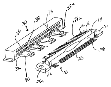
the present invention employs a cormector cover 30 shown in detail in Figures 1, 2A and
2B.
Cover 30 includes an elongate generally rectangular body which is formed of
suitably electrically insulative material which is resistant to the effects of high
temperature soldering. Cover 30 includes a first face 32 shown in detail in Figure 2B and
an opposed second face 34 shown in detail in Figure 2A. Cover 30 includes a plurality of
elongate generally rectangular openings 36 e~ct~n-ling between first face 32 and second
face 34. Openings 36 are designed for alignment with extçntling male pins 18 of header
cormector 10. Cover 30 also includes one or more generally circular apertures 38arranged at various locations on first face 32. Apertures 38 are provided to engage in a
12
. CA 022~4389 1998-11-17 , - -
frictional manner selected pins 18 exten~ling from surface 14a of housing 14 to
frictionally support cover 30 to header connector 10.
Cover 30 further includes a plurality of gripper arms 40 e~t~n(1ing outwardly from
S a lower edge 32a of first face 32. Each gripper arm is an elongate member extending in
cantilevered fashion from edge 32a of first face 32. Each gripper arm includes a beveled
distal extent 41 to facilitate engagement with printed circuit board 12 as will be described
hereinbelow. Proximate of distal extent 41, each gripper arm 40 includes an upwardly
directed bump 43 for providing an area of concentrated engagement with printed circuit
board 12 as will also be described hereinbelow. In the present embodiment, four
longitudinally spaced gripper arms are shown ext~nl1ing from first face 32. However,
fewer or more gripper arms may be employed.
With additional reference to Figs. 4 and 5, cover 30 is designed to be secured to
header connector 10 in a frictional fit manner. The cover 30 is placed over pins 18 of
header connector 10. The first face 32 is positioned against surface 14a of connector 10
so that the pins 18 extend into rectangular openings 36. Frictional engagement is
achieved between selected pins of connector 10 and apertures 38 on first face 32 of
housing 30 to support the cover 30 on cormector 10.
The positioning of gripper arms 40 of cover 30 with respect to connector 10
defines a longitudinal space 42 between gripper arms 40 and solder tails 20 of header
13
CA 022~4389 1998-11-17 '
connector 10. This space is designed for frictional receipt of the edge 12b (Figure 2) of
printed circuit board 12. In use as shown in Figure 2, the ssembled cover 30 andconnector 10, are moved towards printed circuit board 12 in the direction of arrow A.
The edge 12b of printed circuit board is moved into the space 42 (Figure 4) defined
between solder tails 20 and gripper arms 40. Such movement is facilitated by the beveled
distal extent 41 of gripper arm 40. Movement in tnis manner effects mechanical
engagement between header connector 10 and printed circuit 12 and electrical
engagement between solder tails 20 and solder pads 24. The cover 30 of the present
invention is designed in combination with header connector 10 to accommodate a
specified printed circuit board thickness. Thus, the printed circuit board is frictionally
fitted between gripper arm 40 and solder tail 20. Gripper arms 40 extend a sufficient
length along a lower surface 12b of printed circuit board 12 to effectively support header
connector thereon.
The effective connection of printed circuit board 12 to header connector 10 by
employing cover 30 is now shown and described.
Each solder tail 20 generally includes a curved contact surface 21 (Figure 4)
which extends below printed circuit board seating plane P within the space 42 defined
between gripper arms 40 and solder tails 20. In this fashion, the curved surfaces 21 of the
solder tails 20 are positively preloaded onto the solder pads 24 (Figure 2) of printed
circuit board 12 providing superior electrical engagement therewith. The curved surfaces
14
CA 022~4389 1998-11-17
21 of solder tails 20 are positioned in spaced facing opposition to the bumps 43 of gripper
arm 40. The space defined between bumps 43 and curved surfaces 21 is less than the
thickness of the printed circuit board to assure contact pre-loading. Use of spring biased
solder tails allows control of the coplanarity of the solder tails to be relaxed without
sacrificing the ability to make good electrical contact with the solder pads of the printed
circuit board. As mentioned above, it is common that printed circuit boards exhibit
warpage due to ~hrinkAge or ot_er post-mAn~ fActuring conditions. Due to this warpage, it
may become diffficult to mAintAin good electrical contact between all of the solder pads of
the printed circuit board and each of the individual solder tails of the connector. In the
present invention, by employing cover 30 having a plurality of gripper arms 40 w_ich
works in conjunction with header connector 10, the problems of board warpage as well as
other problems of movement of the connector with respect to the board prior to soldering
can be effectively overcome.
Having described the components of the embodiment of Figures 1-7 of the present
invention, its use may be further described.
Referring to Figure 1, cover 30 is attached to header connector 10 with the first
face 32 of cover 30 being positioned against surface 14a of housing 14. Frictional
engagement secures cover 30 to connector 10 by the frictional interfitting of selected pins
18 of header connector 10 with apertures 38 of cover 30. The assembled cover andheader combination as shown in Figure 2 may be brought into engagement with printed
.. .. ..
- CA 022~4389 1998-11-17 -_
- circuit board 12 by movement of printed circuit 12 towards the connector/cover
combination in the direction of arrow A. Upon insertion of board 12 into space 42 along
seating plane P as shown in Figure 4, spring biased electrical engagement is established
between curved surfaces 21 of solder tails 20 and solder pads 24 of board 12 (Figure 2).
The relative dimensions of the printed circuit board 12 and the space between the solder
tails 20 and gripper arms 40 results in spring defection of the solder tails 20 so as to
achieve resilient engagement between the curved surfaces 21 of the solder tails 20 and the
solder pads 24 of printed circuit board 12. The gripper arms 40 m~int~in the solder pads
24 in engagement with the spring biased solder tails 20 correcting for any board warpage
and also preventing disconnection of any of the individual solder tails from the solder
pads during movement of the components during further m~nl~f~cturing procedures.
In the position shown in Figure 5, the solder tails of header connector 10 may be
soldered to the solder pads in a conventional fashion. It is noted that during the soldering
process, the cover 30 is used to secure header connector 10 to the printed circuit board 12.
At this stage, no external securement hardware is necessary. Such securement hardware
may render certain soldering techniques more difficult to practice. Once the solder tails
20 are effectively soldered to solder pads 24, cover 30 may be removed from the
connector/board assembly in a manner shown in Figure 6. The cover 30 is then
discarded. Permanent attachment of header connector 10 to printed circuit board 12 may
now be made by use of appropriate securement hardware (not shown). Such securement
- CA 022~4389 1998-11-17 ~ -
hardware may be positioned through apertures 26a, 28a of ears 26,28 of the header
connector 10 and board 12 resl,e~ ely.
The header connector 10 mounted to printed circuit board 12 is now available formating electrical connection. While any type of mating connector may be mated toheader 10, the present invention in the preferred embodiment shows a ribbon connector
50 tennin~ting a multiconductor ribbon cable 52. The male pins 18 of header connector
10 are accessible for hlterconllection with applop.iately constructed socket contacts 54 of
ribbon connector 50.
A further embodiment of the present invention is shown with respect to Figures 8-
14.
Referring specifically to Figure 8, the present invention may be employed in
combination with a connection assembly referred to as a device bay connection assembly
100. Device bay connection assembly 100 includes a device bay plug 1 10 which isintercormectible to a device bay receptacle 112. The device bay plug 110 includes an
elongate insulative housing 114 (Figure 10) and supports therealong a plurality of
electrical contacts 1 16. Contacts 1 16 have e~ n~ling solder tails 1 18 which are designed
for solder connection to the edge of a printed circuit board in a manner set forth above
with respect to the connector embodiment shown in Figures 1-7.
' -- CA 022~4389 1998-11-17
- Housing 114 further includes a pair of end structures 120 forming the longitudinal
ends of housing 114. End structures 120 have a forward end 121 including an opening
121 a (Figure 14) designed for accom nodating a projection 122 adjacent either
long~ n~l end of receptacle 112 so as to establish aligned interconnection of plug 110
with receptacle 112. Opposed ends 123 of each end structure 120 includes a hold-down
foot 125 for engagement with the printed circuit board in a manner which will bedescribed in further detail hereinbelow.
With additional reference to Figures 9-13, housing 114 includes a first
interconnection face 129 having a pair of longitudinally spaced platforms 130 e~nding
therefrom. Each platform 130 has opposed planar surfaces 130a and 130b (Figure 13).
Contacts 116 of plug 110 include extending connection extents 119 which are
longitudinally spaced along the opposed surfaces 130a and 130b of platforms 130. The
longitudinally spaced platforms 130 including connection extents 119 positioned
therealong, define a pair of longitudinally spaced interconnection engagement arrays 132.
As shown in Figure 8, each engagement array 132 is designed for insertion into an
opening 112a in device bay receptacle 112 placing connection extents 119 in electrical
engagement with electrical contact surfaces 133 of receptacle 112. In this manner,
mechanical and electrical interconnection may be established between device bay plug
110 and device bay receptacle 112.
CA 022~4389 1998-11-17 - -
- Device bay plug 110 is designed to be connected to a printed circuit board 140
along an edge 142 thereof so as to establish electrical connection between solder tails 118
and conductive traces or pads (not shown) on an upper surface 144 of printed circuit
board 140. In order to provide for the mechanical and electrical connection of plug 110
to printed circuit board 140, plug 110 is used in combination with a removable cover 150.
Cover 150, more fully shown in Figure 9, is substantially similar to cover 30
described above with respect to the embo~lim~nt.~ shown in Figures 1-7. Cover 150 is an
elongate, rectangular member formed of suitably electrically insulative material which is
resistant to the effects of high tenlpcldl~lre soldering. Cover 150 includes a first face 152
including a pair of longitudinally spaced cavities 154 and 156. Cavities 154 and 156 are
constructed to accommodate therein the pair of spaced apart engagement arrays 132 of
plug 110. Furthermore the specific configuration of cavities 154 and 156 are designed
such that it provides keyed accommodation of each engagement array 132 of plug 110.
Each cavity 154 and 156 includes an enlarged rectangular portion 154a, 156a in
juxtaposition adjacent the center of cover 150. Such rectangular portions 154a, 156a are
designed to accommodate therein lateral projections 139 adjacent the end of eachengagement array 132. Such keyed interfitting between the rectangular portion of the
cavities and the projections 139 of array 132 provides for proper orientation and
aligmnent of the plug 110 with respect to cover 150. Such engagement also provides for
the removable frictional securement of cover 150 to plug 110.
.. ...
CA 022~4389 1998-11-17 .
.
As described above, cover l S0 also includes a plurality of gripper arms 160
~xten~iing outwardly from a lower edge 152a of first face 152. Each gripper arm 160 is
- an elongate member extending in a cantilevered fashion from edge 152a and includes a
beveled distal extent 153 to facilitate engagement with printed circuit board 140 as will
be described hereinbelow. Each gripper arm 160 also includes an upwardly directed
bump 159 for providing an area of concentrated engagement with printed circuit board
12.
Cover 150 is assembled to plug 110 as shown in Figure 10. The cover 150 is
retained on plug 110 by removable frictional engagement. As shown in Figures 10 and
13, the assembly of the cover 150 and plug 110 define a printed circuit board receiving
space 170 between hold-down feet 125 and gripper arms 160.
As shown in Figure 11, the assembly of the cover l S0 and plug 110 may be
brought towards the edge 142 of printed circuit board 140.
In a manner similar to that described above, solder tails 118 include a curved
contact surface 118a (Figure 13) which would extend into printed circuit board receiving
space 170 defined between hold-down feet 125 and gripper arms 160. This provides a
preload of the solder tails 118 against the upper surface 144 of printed circuit board 140.
Each of the hold-down feet 125 defines a gripping surface 125a which is in spaced
opposition to a gripper arm surface 161 of gripping arms 160. The space 170 so defined
' CA 022~4389 1998-11-17
assures that the contact tails will be preloaded against the upper surface 144 of printed
circuit board 140. This facilitates the accurate soldering of solder tails 118 to the solder
pads of printed circuit board 140.
With respect to the device bay plug 110 shown Figures 8-14, hold-down feet 125
are particularly significant as the contact solder tails 118 are smaller and arranged at a
finer pitch than the connector described above with respect to Figures 1-7. Thus, the
hold-down feet 125 provide stronger surface contact with the printed circuit board
assuring that the printed circuit board is m~int~ined in a planar fashion without warpage.
Use of hold-down feet 125 in combination with the gripper arms 160 assures that no
undue stress will be placed on the fragile solder tails prior to and during the soldering
process.
Having described the components of the embodiment of Figures 8-14 of the
present invention, its use may be further described.
Cover l S0 is ~ hed to plug connector 110 with the first face 152 of cover 150
being inserted over arrays 132 of plug 110. Each array 132 is contained within the
enclosed cavities 154 and 156 of cover 150 where it is protected from contact with dust,
solder paste and other foreign matter during the soldering process. As shown in Figure
14, the opposed second face 155 of cover 150 is closed preventing such foreign matter
from entering thereinto.
21
CA 022~4389 1998-11-17
- Assembled cover and plug as shown in Figure 12 may be brought into
engagement with printed circuit board 140. The printed circuit board 140 is held in the
space 170 defined between hold-down feet 125 of plug 110 and gripper arms 160 of cover
150. In this position the solder tails 118 of contacts 116 are placed in a preloaded
S condition against the upper surface 144 of printed circuit board 140 along edge 142. The
solder tails may then be soldered to the conductive solder pads (not shown) on printed
circuit board 140. During such soldering the engagement arrays 132 of plug 110, that is
the platforms 130 and the contact extents 119 thereon, are completely contained within
the enclosed cavities 154 and 156 of cover 150 and are not exposed to the adverse effects
of the soldering operation.
Once the tails 118 are soldered to printed circuit board 140, the cover 150 may be
removed and discarded. By removing the cover 150 the engagement arrays 132 are
exposed so that device bay plug 110 may be interconnected to device bay receptacle 112
as shown in Figure 8.
Various changes and modifications can be made to the invention, and it is
int.onded to include all such changes and modifications as come within the scope of the
invention as is set forth in the following claims.
. .