Note: Descriptions are shown in the official language in which they were submitted.
CA 02255166 1998-12-16
VOLUME SENSOR FOR PADDLE ELEVATOR USING LASER LIGHT
BACKGROUND OF THE INVENTION
1. Field of the Invention:
The invention is directed to a laser volume sensor used on a combine for
either
detecting the amount of tailings being transported by the tailings elevator,
or the amount of
clean grain being transported by the clean grain elevator.
2. Description of the Prior Art:
Combines are large agricultural machines used to harvest a crop from a field.
After
the crop is harvested by a harvesting platform, the crop material is
transported by a
feederhouse into the interior of the combine. A threshing assembly threshes
the harvested
crop material breaking the grain apart from other grain and/or a husk. Next a
separator
assembly separates the clean grain the crop material other than grain. The
crop material
other than grain is returned to the field, while the grain and entrained small
particles, chaff,
are directed to a cleaning system. The cleaning system cleans the grain
removing the chaff
by blowing the chaff out the rear of the combine. The clean grain is
transported by a clean
grain elevator to a grain tank located on the combine. Photoelectric sensors
for measuring
the volume of clean grain passing through the clean grain elevator have been
proposed, see
German patent 2,445,046.
Sometimes clean grain, unthreshed heads of grain and other crop material pass
over
the sieves of the cleaning system and become tailings. These tailings are
caught before
being expelled from the combine. The tailings are returned to the threshing
assembly by a
tailings elevator. Photodiode sensors for measuring the volume of tailings
passing through
the tailings elevator have also been proposed, see US Patent 4,441,513.
SUMMARY
It is an object of the present invention to provide a laser based sensor for
detecting
the volume of material being conveyed by a paddle conveyor.
It is a feature of the presently invention that the sensor comprises an master
unit and
an opposed slave unit with each unit having a laser and each unit having at
least two photo
detectors. The opposed photo detectors are only triggered when the opposed
laser is fired.
In the preferred embodiment of the sensor, the master and slave units are
substantially identical. In each unit the photo detectors and laser are
arranged in a line with
the laser being located at the highest position in the line. Each photo
detector is provided
with a photo detector circuit that transmits the laser light detection signal
only when the
opposed laser is fired. In this way, laser light detected from the laser
located in the same
unit is not transmitted to the microprocessor.
The master unit is provided with a microprocessor which controls the operation
of the
CA 02255166 1998-12-16
sensor. More specifically, the microprocessor sends out a square wave of high-
low pulses.
The laser is fired on the high pulses and the photo detectors are triggered on
the low pulses.
Therefore when the master unit's laser is fired by a high pulse, the master
unit's photo
detectors are not triggered as they have also received a high pulse.
The slave unit is electrically coupled to the master unit and is provided with
an
inverter that inverts the high-low pulses from the microprocessor. The
inverter essentially
changes the high pulse from the microprocessor to a low pulse and the low
pulse to a high
pulse. In this way when the microprocessor has issued a high pulse, the master
unit's laser
is fired and the opposed slave unit's photo detectors are triggered as the
high pulse has
been inverted into a low pulse. Similarly, when the microprocessor issues a
low pulse, the
master unit's photo detectors are triggered and the opposed slave unit's laser
is fired as the
low pulse has been inverted into a high pulse. It has been found that a
microprocessor
emitting a 400 hertz square wave works well in providing the high-low pulses.
Both the master and slave units are provided with a protective lens of ultra
high
molecular weight polyethylene. This lens extends into the elevator and is
cleaned by the
particulate material passing by the lens.
BRIEF DESCRIPTION OF THE DRAWINGS
Fig. 1 is the right-hand semi-schematic view of an agricultural combine.
Fig. 2 is a partial cross sectional side view of the sensor and its location
in a portion
of the tailings elevator.
Fig. 3 is a perspective view of the master unit of the sensor.
Fig. 4 is an electronic block diagram of the sensor.
Fig. 5 is an electric schematic of the photo detector circuit.
DETAILED DESCRIPTION
Figure 1 shows an agricultural combine 10 comprising a supporting structure 12
having ground engaging means 14 extending from the supporting structure. A
harvesting
platform 16 is used for harvesting a crop and directing it to a feederhouse
18. The harvested
crop is directed by the feederhouse 18 to a beater 20. The beater directs the
crop upwardly
through an inlet transition section 22 to the axial crop processing unit 24.
The axial crop
processing unit is located between the sidesheets of the combine. The
sidesheets form part
of the supporting structure. Although the invention is being described as
being mounted on
a rotary combine, it may also be used on other combines having a clean grain
elevator
and/or a tailings elevator, such as conventional straw walker machines.
The axial crop processing unit 24 comprises an axial rotor housing 26 and an
axial
2
CA 02255166 1998-12-16
rotor 28 located in the housing. The harvested crop enters the housing through
the inlet
transition section 22. The rotor is provided with an infeed portion, a
threshing portion and a
separating portion. The rotor housing has a corresponding infeed section, a
threshing
section and a separating section.
Both crop processing portions of the rotor 28, the threshing portion and the
separating portion, are provided with crop engaging assemblies. The threshing
section of
the rotor housing is provided with a concave and the separating section is
provided with a
grate. Grain, including unthreshed heads of grain, chaff and other crop
material are
released from the crop mat and fall through the concave and the grate to the
cleaning
system. Larger crop material is expelled out the rear of the axial crop
processing unit by
beater 30.
As illustrated in Figure 1, grain and chaff falling through the concave and
grate is
directed to cleaning system 34 which removes the chaff from the grain. The
cleaning system
is provided with a blower that blows chaff out the rear of the combine. The
heavier clean
grain is collected by a transverse clean grain auger which directs the clean
grain to a clean
grain paddle elevator 36. The paddle elevator 36 directs the grain upwardly to
a transition
housing 38 where the grain is supplied to a loading auger 40 for loading the
clean grain tank
42. The grain is removed from the clean grain tank 42 by unloading auger 44.
Similarly,
clean grain not falling through the sieves, unthreshed heads of grain and
other crop material
form tailings that are collected by a tailings cross auger which directs the
tailings to a tailing
paddle elevator 46. As best illustrated in Figure 2, the tailing paddle
elevator is provided
with a series of chain driven paddles 47 on which the tailings are
transported. The tailing
paddle elevator 46 directs the tailings to a tailings cross auger located
adjacent to the
threshing portion of the axial separator for injecting the tailings back into
the crop processing
unit. The operation of the combine is controlled from operator's cab 48. A
radio receiver 50
for receiving GPS signals is positioned over the operator's cab so that the
sensor data from
the sensor can be combined with the GPS signal data to provide a crop mapping
option.
The following description of the preferred embodiments directed to a volume
sensor
located in the tailings elevator of the combine. However it should be noted,
that the sensor
could also be located in the clean grain elevator. The sensor uses laser light
to sense the
crop material piled on the individual paddles as they pass the sensor's
location. The sensor
of the present invention could be used for measuring the volumetric flow rate
(VFR) of any
type of granular or particulate matter as it passes is conveyed by a paddle
conveyor.
It is advantageous to the farmer or combine operator to have an indication of
the
3
CA 02255166 1998-12-16
amount of tailings and/or clean grain that is being conveyed by the elevator
systems of the
combine so as to avoid jamming and to assist in maintaining proper combine
adjustments.
Further, it is beneficial to have a volumetric measurement (as opposed to
another
measurement, such as mass), since crop yield is measured in bushels, which is
a volumetric
measurement.
The volume sensor 60 is mounted to the tailings elevator comprises two units,
a
master unit 62 and a slave unit 64. These units are mounted on either side of
the enclosure
of the tailings elevator 46 and are substantially parallel to and opposed to
each other. Each
unit is provided with a laser light emitting diode 66 (e.g., but not limited
to, EG&G
Optoelectronics C86137E or Siemens type SPL PL85) and four light emitting
diodes forming
photo detectors 68. The laser diode 66 and the photo detectors 68 are arranged
in a line
parallel to the elevator paddles. The laser diode 66 being the highest and the
four photo
detectors 68 extending downwardly therefrom. By having the laser diodes
located at the
highest point and opposed to one another the transverse slope of the tailings
pile on the
paddle can be sensed. By knowing the side profile of the material, the width
of the elevator
enclosure, and the time and distance between each paddle the volumetric flow
rate of the
tailings material can be predicted.
The sensor 60 is housed in a box 70 having an open side. The open side of the
box
is the surface that abuts the outside enclosure of the tailings elevator. A
portion of the open
side is provided with a faceplate 72 with the remaining portion of the circuit
board is potted
sealing the box 70. The face plate 72 is formed from an ultra-high molecular
weight
polyethylene (UHMWP), which is designed for high wearability and abrasion
resistance. The
selected UHMWP also has the appropriate optical properties, i.e., it is
diffusing and the index
of refraction = 1.54 (unitless). The laser diode 66 and the photo detectors 68
are positioned
as close to or in direct contact with the rear of the faceplate 72 facing
outwardly therefrom.
The faceplate forming a protective lens for the laser diode and the photo
detectors. It has
been found that the thickness of the faceplate 72 may effect the output of the
laser diode 66
as detected by the opposed photo detectors 68. It has been found that a
faceplate of 2.0
millimeters thickness works satisfactory.
The face plate is formed with a raised boss 74 forming the protective lens for
the
laser diode 66 and the photo detectors 68. The box 70 is mounted onto the
exterior surface
of the tailings elevator 46 by mounting bolts 73, in such a manner that the
raised boss 74 fits
through a cutout in the tailings elevator. The tailings elevator 46 being
large enough to
accommodate the size and shape of the raised boss 74. The raised boss 74 is
designed
4
CA 02255166 1998-12-16
such that it is thicker than the sheet metal comprising the tailings elevator
enclosure (e.g.,
twice as thick as the sheet metal). This design allows increased exposure of
the face of the
raised boss to the tailings material, which acts as a self cleaning mechanism
for the sensor
face. The raised boss 74 is provided with tapered edges 76 in order to prevent
a sharp edge
inside the elevator 46.
Each of the laser diodes 66 emits a pulsed infrared or near-infrared light
(e.g., 905
nm). The laser diodes 66 are pulsed incrementally at a predefined frequency of
400 hertz.
When the laser diodes 66 are pulsed, the emitted light is coherent, with a
gaussian spatial
distribution. The light illuminates the entire inner chamber of the unblocked
tailings elevator
between the firing laser and the opposed triggered photo detectors.
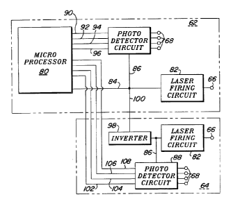
Fig. 4 is a block diagram of the volume sensor electronics. The master unit is
provided with a microprocessor 80 which is powered by a conventional power
supply. The
microprocessor is programmed to emit a 400 hertz high-low square wave pulse to
the
master unit's laser firing circuit 82 through line 84. Line 86 taps into line
84 and couples the
master unit's photo detector circuit 88 the 400 hertz output of the
microprocessor. As
discussed above when the laser firing circuit 82 receives a high pulse the
laser is fired.
When photo detector circuit 88 receives a high pulse the photo detector
circuit 88 is not
triggered and no output is received from the master unit's photo detector
circuit. Similarly, if
a low pulse is received by the laser firing circuit 82, the laser is not
fired. The low pulse
triggers the photo detector circuit 88 detecting light emitted from the slave
unit's laser, if not
blocked by tailings, and sending that information back to the microprocessor
via lines 90,
92, 94 and 96.
The slave unit is provided with an inverter 98 that inverts the 400 hertz high-
low
square wave received on line 100 making high pulses low pulses and low pulses
high
pulses. As with the master unit the laser firing circuit 82 of the slave unit
is fired by high
pulses and the photo detector circuit 88 is triggered by low pulses. As these
pulses are
inverted by the inverter 98, a high pulses from microprocessor 80, fires the
master unit's
laser firing circuit 82 and triggers the slave unit's photo detector circuit
88. The detected
information by the slave unit's photo detectors 68 is transmitted back to the
microprocessor
80 along lines 102, 104, 106, and 108. A low pulse from the microprocessor
triggers the
master unit photo detector circuit 88 and fires the slave unit's laser firing
circuit 82.
The laser firing circuits for the master unit and the slave unit are of a
conventional
configuration. The photo detector circuits for the master and slave units are
substantially
identical with the photo detector circuit for one of the photo detectors being
illustrated in
5
CA 02255166 1998-12-16
Figure 5. Each photo detector is provided with an photo amplifier 110
amplifying the
resulting signal from the photo detector, a second stage amplifier 112 further
amplifying the
signal, an analog to digital converter 114 for converting the analog signal to
a digital signal,
and a logic circuit 116 for directing the digitized output signal to the
microprocessor when the
logic circuit receives a low pulse.
The photo diode LED1 produces a negative current pulse when it detects light.
This
signal is amplified by photo amplifier 110 with a gain of 100 resulting in a
positive voltage
pulse. This positive voltage pulse is amplified by second stage amplifier 112
with a gain of
100 into a negative voltage pulse that is directed to analog to digital
converter 114. The
digitized signal is directed to the logic circuit 116 where it is inverted by
inverter U4 and
applied to flip flop U5. Flip flop U5 signals the microprocessor via an
appropriate line (90,
92, 94, 96, 102, 104, 106 or 108) as to the presence of laser light detected
by the photo
diode LED 1 when the flip flop receives a low pulse via line 86 directly from
the
microprocessor 80 for the master unit or from the inverter 98 for the slave
unit.
The components of a single photo detector channel are listed in Table 1 and
are
disclosed as an example of a suitable circuit for the present application
Table 1
C1, C4 0.1 micro farad 50 Volt Package Style 08 capacitor
C2 1000 pico farad 50 volt package style 08 capacitor
C3 5 pico farad 50 volt package style 08 capacitor
C5 15 pico farad 50 volt package style 08 capacitor
R1 4.99K ohms 1/10 watt 1% resistor
R2, R8 30.1 K ohms 1 /10 watt 1 % resistor
R3, R5, R9 1 OOK ohms 1 /10 watt 1 % resistor
R4, R6 1.OK ohms 1/10 watt 1% resistor
R7 243K ohms 1/10 watt 1% resistor
R10 10K ohms 1/10 watt 1% resistor
U1, U2 1/4 operational amplifier Motorola MC33074D
U3 1/4 operational amplifier National LM2901
U4 1/4 Hex inverter Motorola MX74HC14
U5 1/2 Dual D Flip Flop with set/reset MC74HC74AD
6
CA 02255166 1998-12-16
It should again be noted that Figure 5 represents one photo detector channel
for one
photo detector. The operational amplifiers U1, U2, U3 and the inverter U4 are
shared
among the other photo detectors in the photo detectors respective master or
slave unit.
Similarly half the dual flip flop is shared by the adjoining photo detector
and another flip flop
is provided for the two remaining photo detectors in the respective master or
slave unit.
The present invention should not be limited to the above described embodiments
but
should be limited solely to the claims that follow.
7