Note: Descriptions are shown in the official language in which they were submitted.
CA 02255350 1998-12-09
1
A Data Processing Apparatus and its Data Processing Method
Background of the Invention
Field of the Invention
This invention relates to a data processing apparatus
with an input/output (I/O) device and its data processing
method.
Description of the Related Art
An I/O device, e.g., disk controller, network
controller, etc. is usually connected to a bus. Since a
number of devices connectable to a bus is restricted by an
electrical condition of the bus, number of control signals,
etc., the number of the devices connected to the bus is
limited.
The number of devices connectable to the bus can be
increased by layering the bus. The layered bus is called as
a hierarchical bus, hereinafter. In the hierarchical bus, a
bus coupler is provided between a bus at an upper layer and
a bus at a lower layer. The bus coupler relays data from a
bus to an appropriate bus based on a destination address of
the data transmitted in the bus.
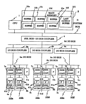
Fig. 23 illustrates a data transfer system with the
hierarchical bus according to the related art. In Fig. 23,
disk controllers and magnetic disk drives (or also called as
disk drives, hereinafter) controlled by the disk controllers
are provided as the I/O devices for example. Normally, an
origin or destination of a data transfer is a main memory,
and the main memory is shared by all the I/O devices.
Therefore, the main memory is connected to a top layer in
the hierarchical bus.
Operations are explained with reference to Fig. 23.
__._..__.~.._.__.__.._.~.._._...
CA 02255350 1998-12-09
2
Data in files 61a - 61f in disk drives 8a - 8f are
transferred to buffers l0a - lOf in a main memory 2, and
processed by a central processing unit (CPU) 1.
The CPU 1 requests a disk controller 7a to transfer the
data in the file 61a in the disk drive 8a to the buffer 10a.
The disk controller 7a transfers the data to an I/0 bus 5a.
An I/O bus coupler 6a relays the data from the I/0 bus 5a to
an I/0 bus 5d. A system bus - I/0 bus coupler 4 relays the
data from the I/O bus 5d to a system bus 3. Then, the data
are stored in the buffer l0a in the main memory 2.
The CPU 1 also requests a disk controller 7b to
transfer the data in the file 61b in the disk drive 8b to
the buffer lOb. The disk controller 7b transfers the data
to the I/O bus 5a. The I/O bus coupler 6a relays the data
from the I/O bus 5a to the I/O bus 5d. The system bus - I/O
bus coupler 4 relays the data from the i/O bus 5d to the
system bus 3. Then, the data are stored in the buffer lOb
in the main memory 2.
The CPU 1 also requests a disk controller 7c to
transfer the data in the file 61c in the disk drive 8c to
the buffer lOc. The disk controller 7c transfers the data
to an I/O bus 5b. An I/O bus coupler 6b relays the data
from the I/O bus 5b to the I/O bus 5d. The system bus - I/0
bus coupler 4 relays the data from the I/O bus 5d to the
system bus 3. Then, the data are stored in the buffer lOc
in the main memory 2.
The CPU 1 also requests a disk controller 7d to
transfer the data in the file 61d in the disk drive 8d to
the buffer lOd. The disk controller 7d transfers the data
to the I/O bus 5b. The I/O bus coupler 6b relays the data
from the I/0 bus 5b to the I/O bus 5d. The system bus - I/O
bus coupler 4 relays the data from the I/O bus 5d to the
_.______. ._..._~~_. _ _._._. _
_ CA 02255350 1998-12-09
3
system bus 3. Then, the data are stored in the buffer lOd
in the main memory 2.
The CPU 1 also requests a disk controller 7e to
transfer the data in the file 61e in the disk drive 8e to
the buffer 10e. The disk controller 7e transfers the data
to an I/O bus 5c. An I/O bus coupler 6c relays the data
from the I/O bus 5c to the I/O bus 5d. The system bus - I/0
bus coupler 4 relays the data from the I/0 bus 5d to the
system bus 3. Then, the data are stored in the buffer l0e
in the main memory 2.
The CPU 1 also requests a disk controller 7f to
transfer the data in the file 61f in the disk drive 8f to
the buffer lOf. The disk controller 7f transfers the data
to the I/O bus 5c. The I/O bus coupler 6c relays the data
from the I/O bus 5c to the I/O bus 5d. The system bus - I/O
bus coupler 4 relays the data from the I/O bus 5d to the
system bus 3. Then, the data are stored in the buffer lOf
in the main memory 2.
The CPU 1 processes the data transferred to the buffers
l0a - lOf, and stores a result from processing in a last
output buffer 101.
As stated, the data are always transferred to the main
memory 2 via the I/0 bus 5d, system bus - I/O bus coupler 4,
and system bus 3. The data transferred from all the I/0
devices connected at lower layers in the hierarchical bus
are channeled through the buses at upper layers in the
hierarchical bus.
However, since a data transfer amount in a bus per a
unit time period is generally limited, data exceeding the
limit cannot be transferred.
When a bus is occupied for a transfer of data, even if
a transfer of other data is requested, the latter data
cannot be transferred until the first data transfer is
CA 02255350 1998-12-09
4
completed. When the data in the files 61a - 61e are
transferred at once, a transfer speed of the data is
restricted by transfer speeds of data in the I/O bus 5d and
system bus 3. Therefore, even if the number of connectable
devices is increased by adopting the hierarchical bus, a
data transfer speed of the system is restricted by a
transfer speed of the bus at the top layer. Hence, a data
transfer speed appropriate for the number of devices cannot
be realized.
In the hierarchical bus according to the related art,
the CPU 1 processes all the data. Since a data amount
processed by the CPU per a unit time period is limited, data
exceeding the limit cannot be processed. When the CPU 1
processes the data transferred from the files 61a - 61e, a
processing speed of the data is restricted by a processing
speed of the CPU 1. Even if a number of connectable devices
is increased by adopting the hierarchical bus, a processing
speed of the system is restricted by the processing speed of
the CPU, and a data processing speed appropriate for the
number of devices cannot be realized.
The hierarchical bus according to the related art is
configured as above stated, and all the transferred data are
channeled through the buses at upper layers. Therefore,
even if the number of connectable devices is increased, an
appropriate data transfer speed cannot be realized.
The hierarchical bus according to the related art is
configured as above stated, and the processing speed of data
is restricted by the processing speed of the CPU.
Therefore, even if the number of connectable devices is
increased, an appropriate processing speed cannot be
realized.
Summary of the Invention
_ CA 02255350 1998-12-09
S
It is an object of this invention to solve the above-
stated problems in the related art. Particularly, this
invention aims at increasing the number of connectable
devices by adopting the hierarchical bus and improving a
S transfer speed when the number of the devices is increased.
This invention also aims at increasing the number of
connectable devices by adopting the hierarchical bus and
improving a processing speed when the number of the devices
is increased.
According to one aspect of this invention, a data
processing apparatus includes an upper~bus and a lower bus
connected hierarchically, a memory connected to the upper
bus, a device connected to the lower bus, a processor,
connected to the0lower bus, for receiving data from the
device via the lower bus, extracting a part of the received
data, and transferring the extracted data to the memory via
the upper bus, and a processing unit connected to the upper
bus for processing the transferred data in the memory.
According to another aspect of this invention, a data
processing method includes the steps of transferring data
from the device to the processor via the lower bus,
extracting a part of the transferred data by the processor,
transferring the extracted data to the memory via the upper
bus, and processing the transferred data in the memory by
the processing unit.
Further features and applications of the present
invention will become apparent from the detailed description
given hereinafter. However, it should be understood that
the detailed description and specific examples, while
indicating preferred embodiments of the invention, are given
by way of illustration only, since various changes and
modifications within the spirit and scope of the invention
_ _..~..~.~___ _._ ~..~.._
- CA 02255350 1998-12-09
6
will become apparent to those skilled in the art from this
detailed description.
Other objects features, and advantages of the invention
will be apparent from the following description when taken
in conjunction with the accompany drawings.
Brief Description of the Drawings
Fig. 1 shows a system configuration chart in an
embodiment of this invention;
Fig. 2 shows a configuration chart of a system bus -
I/O bus coupler in an embodiment of this invention;
Fig. 3 shows a configuration chart of an.I/O bus
coupler in an embodiment of this invention;
Fig. 4 shows a configuration chart of a processor in an
embodiment of this invention;
Fig. 5 illustrates an address distribution in a
physical address space in an embodiment of this invention;
Fig. 6 illustrates an address translation by a
processor in an embodiment of this invention;
Fig. 7 illustrates a configuration of a file in an
embodiment of this invention;
Fig. 8 illustrates a configuration of a block
constituting a file in an embodiment of this invention;
Fig. 9 illustrates a sample of a first accumulation and
a result from the first accumulation in an embodiment of
this invention;
Fig. 10 illustrates an internal configuration in a
first accumulation in an embodiment of this invention;
Fig. 11 illustrates a sample of a selection -
projection processing and its result from the selection
projection processing in an embodiment of this invention;
Fig. 12 illustrates a sample of a block accumulation
processing and its result from the first accumulation in an
embodiment of this invention;
- CA 02255350 1998-12-09
7
Fig. 13 illustrates a sample of a second accumulation
and its result from the second accumulation in an embodiment
of this invention;
Fig. 14 illustrates an accumulation processing in an
embodiment of this invention;
Fig. 15 shows a flow chart of operations in an
embodiment of this invention;
Fig. 16 shows a system configuration chart in another
embodiment of this invention;
Fig. 17 shows a configuration chart of an I/O bus
coupler with a processor in another embodiment of this
invention;
Fig. 18 shows a system configuration chart in another
embodiment of this invention;
Fig. 19 illustrates an accumulation processing in
another embodiment of this invention;
Fig. 20 illustrates an accumulation processing in
another embodiment of this invention;
Fig. 21 shows a flow chart of operations in another
embodiment of this invention;
Fig. 22 illustrates a hierarchical accumulation
processing in another embodiment of this invention; and
Fig. 23 shows a system configuration chart according to
the related art.
Detailed Description of the Preferred Embodiments
Embodiment 1.
Fig. 1 illustrates a configuration of a system for
realizing an embodiment of this invention.
In Fig. 1, the central processing unit (CPU) 1 controls
each unit in the whole system. The main memory 2 is also
illustrated. The system bus 3 is a channel for a data
transfer between the CPU 1 and the main memory 2 and a data
transfer between the system bus - I/O bus coupler 4 and the
.... ........_.~.....~_....,.._ ._.._......T....r........... ....... ..,_...
_ CA 02255350 1998-12-09
g
main memory 2. The system bus - I/0 bus coupler 4 relays
data transferred between a device connected to an I/O bus
and a device connected to the system bus. An I/O device,
e.g., disk controller, etc. or bus coupler is connected to
the I/O buses 5a - 5d. The I/0 buses 5a - 5d are controlled
in a different procedure from the system bus 3. Each of the
I/0 bus couplers 6a - 6c is connected to two of the I/0
buses for relaying the data transferred between I/0 devices
or bus couplers connected to the different I/0 buses. The
system bus 3 and all the I/0 buses 5a - 5d are assumed to
have a same physical address space.
Each of I/O devices 102a - 102f includes a disk
controller and a magnetic disk drive. The disk controllers
7a - 7f control the magnetic disk drives (or also called as
disk drives) 8a - 8f respectively. Processors 9a - 9c are
provided. The buffers l0a - lOc are provided in the main
memory 2. The files 61a - 61f are stored in the disk drives
8a - 8f respectively. The last output buffer 101 is also
provided in the main memory 2.
Fig. 2 illustrates a configuration of the system bus -
I/O bus coupler 4 according to this embodiment.
In Fig. 2, the system bus 3 and the I/O bus 5d are
illustrated. A system bus interface 11, an I/O bus
interface 12, and buffers 13 and 14 are also illustrated.
When data are transferred from the I/O bus 5d to the system
bus 3, the data are stored in the buffer 13 temporarily.
When data are transferred from the system bus 3 to the I/O
bus 5d, the data are stored in the buffer 14 temporarily. A
physical address range of the I/O bus 5d is stored in an I/O
bus physical address range register 15. A physical address
can be assigned to the I/O bus 5d by providing the physical
address range of the I/0 bus 5d in the I/O bus physical
address range register 15.
.. ~..~.___. _...~..._... .~._
CA 02255350 1998-12-09
9
When a request of transfer for the physical address
range provided in the I/0 bus physical address range
register 15 is transmitted to the system bus 3, the system
bus - I/O bus coupler 4 responds to the request. If the
request is a transfer of data from the system bus 3 to the
I/O bus 5d, the system bus interface 11 responds to the
request in the system bus 3, and stores the data sent from
the system bus 3 in the buffer 14. Then, the data are
transferred to the I/0 bus 5d via the I/0 bus interface 12.
If the request is a transfer of data from the I/O bus 5d to
the system bus 3, the I/0 bus interface 12 relays the
request of transfer for the address range assigned to the
I/O bus 5d, and receives a transferring data from the I/O
bus 5d. Then, the data are stored in the buffer 13, and
transferred to the system bus 3 via the system bus interface
11. The system bus - I/O bus coupler 4 doesn't respond to a
request of transfer in the system bus 3 for a physical
address range which is not provided in the I/0 bus physical
address range register 15.
However, when a request of transfer for a physical
address range which is not provided in the I/O bus physical
address range register 15 is transferred to the I/O bus 5d,
the system bus - I/O bus coupler 4 responds to the request.
If the request is a transfer of data from the I/O bus 5d to
the system bus 3, the I/0 bus interface 12 responds to the
request in the I/O bus 5d, and stores the data sent from the
I/0 bus 5d in the buffer 13. Then, the data are transferred
to the system bus 3 via the system bus interface 11. If the
request is a transfer of data from the system bus 3 to the
I/O bus 5d, the system bus interface 11 relays the request
of transfer for the address range assigned to the system bus
3, and receives the data from the system bus 3. Then, the
data are stored in the buffer 14, and transferred to the I/O
- CA 02255350 1998-12-09
bus 5d via the I/O bus interface 12. The system bus - I/O
bus coupler 4 doesn't respond to a request of transfer in
the I/O bus 5d for a physical address range which is
provided in the I/0 bus physical address range register 15.
5 Fig. 3 illustrates a configuration of the I/O bus
coupler 6a according to this embodiment. Configuration of
the I/O bus couplers 6b and 6c is same as Fig. 3.
In Fig. 3, the I/0 bus 5d at an upper layer and the I/0
bus 5a at a lower layer are illustrated. An upper bus
10 interface 21, a lower bus interface 22, and buffers 23 and
24 are also illustrated. Data transferred from the I/O bus
5a at the lower layer to the I/O bus 5d at the upper layer
is temporarily stored in the buffer 23. Data transferred
from the I/O bus 5d at the upper layer to the I/0 bus 5a at
the lower layer is temporarily stored in the buffer 24. A
physical address range of the I/O bus 5a at the lower layer
is stored at a lower layer I/O bus physical address range
register 25 temporarily. A physical address can be assigned
to the I/0 bus 5a at the lower layer by providing a physical
address range of the I/O bus 5a at the lower layer in the
I/0 bus physical address range register 25.
The I/O bus coupler 6a responds to the request of
transfer of the data in the I/O bus 5d at the upper layer
for a physical address range provided in the lower layer I/O
bus physical address range register 25. If the request is a
transfer of the data from the I/O bus 5d at the upper layer
to the I/O bus 5a at the lower layer, the upper bus
interface 21 responds to the request of transfer of the data
in the I/O bus 5d at the upper layer, and stores the data
transferred from the I/O bus 5d at the upper layer in the
buffer 24. Then, the data are transferred to the I/0 bus 5a
via the lower bus interface 22. If the transfer of the data
is from the I/0 bus 5a at the lower layer to the I/O bus 5d
- CA 02255350 1998-12-09
11
at the upper layer, the lower bus interface 22 relays the
request of transfer for the concerning address to the I/O
bus 5d, and receives the transferring data from the I/O bus
5a at the lower layer. Then, the data are stored in the
buffer 23. The data are transferred to the I/O bus 5d at
the upper layer via the upper bus interface 21. The I/0 bus
coupler 6a doesn't respond to a request of transfer for a
physical address range which is not provided in the I/0 bus
physical address range register 25 in the I/O bus at the
upper layer.
The system bus - I/O bus coupler 4 responds to a
request of transfer in the I/O bus 5a at the lower layer for
the physical address range besides the physical address
range provided in the lower layer I/O bus physical address
range register 25.
If the transfer of the data is from the I/O bus 5a at
the lower layer to the I/0 bus 5d at the upper layer, the
lower bus interface 22 responds to the request of transfer
of the data in the I/O bus 5a at the lower layer, and stores
the data transferred from the I/O bus 5a at the lower layer
in the buffer 23. Then, the data are transferred to the I/0
bus 5d at the upper layer via the upper bus interface 21.
If the transfer of the data is from the I/O bus 5d at the
upper layer to the I/O bus 5a at the lower layer, the upper
bus interface 21 relays the request of transfer for the
concerning address to the I/0 bus 5d at the upper layer, and
receives the transferring data from the I/0 bus 5d at the
upper layer. The data are stored in the buffer 24 once, and
transferred to the I/0 bus 5a at the lower layer via the
lower bus interface 22. The I/O bus coupler 6a doesn't
respond to a request of transfer for the physical address
range provided in the lower layer I/O bus physical address
range register 25.
- CA 02255350 1998-12-09
12
Fig. 4 illustrates a configuration of the processor 9a
according to this embodiment. Configuration of the
processors 9b and 9c is same as Fig. 4.
In Fig. 4, the I/O bus 5a is illustrated. The
processor 9a is connected to the I/O bus 5a. An I/O bus -
local bus coupler 30 is provided for performing a data
transfer between an I/O device or bus coupler connected to
the I/O bus and a microprocessor 32, local memory 33 or DMA
(Direct Memory Access) controller 36 connected to a local
bus 31. The local bus 31 has a local address space
different from the I/O bus 5a. The microprocessor 32 and
the local memory 33 are also illustrated. The local memory
33 functions as a main memory of the microprocessor 32. An
address translator 34 performs an address translation of the
physical address in the I/O bus 5a and a local address in
the local bus 31 for performing a data transfer between the
I/O bus 5a and the local bus 31, which have different
address spaces. A physical address range register 35 is
also illustrated. A physical address range can be assigned
to the processor 9a by providing the physical address range
in the physical address range register 35. Input buffers
37a and 37b are provided in the local memory 33, and output
buffer 38a and 38b are provided in the local memory 33.
Fig. 5 illustrates an address distribution in a
physical address space according to this embodiment.
A whole physical address space 41 is illustrated. A
physical address range 42 in the physical address space is
assigned to the system bus 3, and a physical address range
43 in the physical address space is assigned to the main
memory 2.
In Fig. 5, a physical address range 44a in the physical
address space is assigned to the I/O bus 5a. A physical
address range 45a in the physical address range 44a of the
- CA 02255350 1998-12-09
13
I/O bus 5a is assigned to the processor 9a. Physical
address ranges 46a and 46b in the physical address range 45a
of the processor 9a are assigned to the input buffers 37a
and 37b in the local memory 33. Physical address ranges 47a
and 48b in the physical address range 45a of the processor
9a are assigned to the output buffer 38a and 38b in the
local memory 33.
In Fig. 5, a physical address range 44b in the physical
address space is assigned to the I/O bus 5b. A physical
address range 45b in the physical address range 44b of the
I/O bus 5b is assigned to the processor 9b. Physical
address ranges 46c and 46d in the physical address range 45b
of the processor 9b are assigned to the input buffers 37a
and 37b in the local memory 33. Physical address ranges 47c
and 47d in the physical address range 45b of the processor
9b are assigned to the output buffers 38a and 38b in the
local memory 33.
In Fig. 5, a physical address range 44c in the physical
address space is assigned to the I/O bus 5c. A physical
address range 45c in the physical address range 44c of the
I/O bus 5c is assigned to the processor 9c. Physical
address ranges 46e and 46f in the physical address range 45c
of the processor 9c are assigned to the input buffers 37a
and 37b in the local memory 33. Physical address ranges 47e
and 47f in the physical address range 45c of the processor
9c are assigned to the output buffers 38a and 38b in the
local memory 33.
In Fig. 5, a physical address range 48a in a physical
address range 43 of the main memory 2 is assigned to the
buffer 10a. A physical address range 48b in the physical
address range 43 of the main memory 2 is assigned to the
buffer lOb. A physical address range 48c in the physical
address range 43 of the main memory 2 is assigned to the
CA 02255350 1998-12-09
14
buffer lOc. A physical address range 48d in the physical
address range 43 of the main memory 2 is assigned to the
buffer lOd. A physical address range 48e in the physical
address range 43 of the main memory 2 is assigned to the
buffer 10e. A physical address range 48f in the physical
address range 43 of the main memory 2 is assigned to the
buffer lOf. A physical address range 48g in the physical
address range 43 of the main memory 2 is assigned to the
last output buffer 101.
Fig. 6 shows an address translation in the processor 9a
according to this invention.
In Fig. 6, the physical address space 41 and the local
address space 51 in the local bus 31 are illustrated. The
physical address range 45a provided in the physical address
range register 35 is translated to a local address range 55
by the address translator 34. Data in the input buffer 37a
is in the physical address range 46a in the physical address
space 41 of the I/O bus and in a local address range 56a in
the local address space 51 of the local bus at the same
time. Data in the input buffer 37b is in the physical
address range 46b in the physical address space 41 of the
I/0 bus and in a local address range 56b in the local
address space 51 of the local bus at the same time. Data in
the output buffer 38a is in the physical address range 47a
in the physical address space 41 of the I/O bus and in a
local address range 57a in the local address space 51 of the
local bus at the same time. Data in the output buffer 38b
is in the physical address range 47b in the physical address
space 41 of the I/O bus and in a local address range 57b in
the local address space 51 of the local bus at the same
time.
CA 02255350 1998-12-09
Fig. 7 illustrates a data format of the file 61a
according to this embodiment. Formats of the files 61b -
61f are same as the file 61a.
The file 61a includes a plurality of blocks 62a - 62d,
5 etc. Sizes of the blocks 62a - 62d, etc. and sizes of the
input buffers 37a and 37b are all same.
Fig. 8 illustrates a data format of the block 62a in
the file 61a according to this embodiment. Formats of the
blocks 62b - 62d, etc. are same as the block 62a.
10 In Fig. 8, the block 62a includes a plurality of
records 63a - 63m, etc. Each of the records 63a - 63m, etc.
includes data in a key field 64, numeric field 65, date
field 66, etc.
Fig. 9 illustrates a sample of a first accumulation and
15 a result from the first accumulation.
In Fig. 9, a first accumulation 71a and a result 72a
from the first accumulation of the block 62a are
illustrated. The result 72a from the first accumulation
includes first accumulation records 73a - 73d. Each of the
first accumulation records 73a - 73d includes data in a
first accumulation key field 74 and a first accumulation
numeric field 75. In this embodiment, data in the numeric
field 65 with data in the date field 66 of May, 1998 are
accumulated for each kind of data in the key field 64 in the
first accumulation.
Fig. 10 illustrates operations in the first
accumulation according to this embodiment.
In Fig. 10, the first accumulation 71a is illustrated.
The block 62a is an input to the first accumulation 71a.
The result 72a from the first accumulation 71a is an output
from the first accumulation 71a. The first accumulation 71a
includes steps of selection - projection 76 and block
accumulation 77. A result 67 from the selection -
- CA 02255350 1998-12-09
16
projection 76 is an output from the selection - projection
76 and becomes an input to the block accumulation 77.
Fig. 11 illustrates a sample of the selection
projection 76 and the result 67 from the selection
projection 76 according to this embodiment.
In Fig. 11, the selection - projection 76 and the
result 67 from the selection - projection 76 of the block
62a are illustrated. Post - selection - projection records
163c - 163I are illustrated. Each of the post - selection -
projection records 163c - 163i includes data in the key
field 64 and the numeric field 65.
In this embodiment, records 63c - 63i with data in the
date field 66 of May 1998 are selected, and data in the key
field 64 and numeric field 65 of the records 63c - 63i are
extracted or projected for generating the post - selection -
projection records 163c - 163i respectively. The post -
selection - projection records 163c - 163i are the result 67
from the selection - projection.
Fig. 12 illustrates a sample of the block accumulation
77 and its result 72a from the first accumulation according
to this embodiment.
In Fig. 12, the block accumulation 77 and the result
72a from the first accumulation, i.e., the result 72a from
the block accumulation 77 of the result 67 from the
selection - projection, are illustrated. In the block
accumulation. 77, data in the numeric field of records are
accumulated for each kind of data in the key field 65, and
the first accumulation records 73a - 73d are generated. In
Fig. 12, the first accumulation record 73a is generated from
the post - selection - projection records 163c and 163h, the
first accumulation record 73b is generated from the post -
selection - projection records 163d, 163g, and 1631, the
first accumulation record 73c is generated from the post -
- CA 02255350 1998-12-09
17
selection - projection record 163e, and the first
accumulation record 73d is generated from the post -
selection - projection record 163f.
Fig. 13 illustrates a sample of a second accumulation
81 and a result 82 from the second accumulation 81 according
to this embodiment.
In Fig. 13, the result 72a from the first accumulation
and a previous result 82a from the second accumulation 81
are illustrated. The result 82 from the second accumulation
of the result 72a from the first accumulation and the
previous result 82a from the second accumulation 81 is
illustrated. The previous result 82a from the second
accumulation includes second accumulation records 83a - 83d,
and the result 82 from the second accumulation includes
second accumulation records 83e - 83i. Each of the second
accumulation records 83a - 83d and 83e - 83i includes data
in a second accumulation key field 84 and a second
accumulation numeric field 85.
Fig. 14 illustrates a sample of an accumulation
processing according to this embodiment.
In Fig. 14, files 61a - 61f include blocks 62a - 62d,
etc. First accumulations 71a - 71f of the files 61a - 61f
are illustrated. The first accumulations 71a and 71b are
performed by the processor 9a, the first accumulations 71c
and 71d are performed by the processor 9b, and the first
accumulation 71e and 71f are performed by the processor 9c.
The results 72a - 72d, etc. from the first accumulation 71a
of the blocks 62a - 62d, etc. are obtained. The results
from the same first accumulation, e.g., 72a - 72d, etc. are
generally called as a first accumulation result sequence.
First accumulation result sequences 92a - 92f are sets of
the results from the first accumulations 71a - 71f. A queue
91 for the result from the first accumulation is also
- CA 02255350 1998-12-09
18
illustrated. The second accumulation 81 and the result 82
from the second accumulation 81 are also illustrated.
Fig. 15 shows a flow chart of operation of an
accumulation processing according to this embodiment. The
operations are shown in steps SO - S8.
Operations are explained.
For a purpose of explanation of this embodiment, data
in the numeric field 65 are accumulated for each kind data
in the key field 64 in the files 61a - 61f stored in the
magnetic disk drives 8a - 8f, and the result 82 from the
second accumulation is obtained as a final processing
result.
The CPU 1 provides the physical address range 44a in
the lower layer I/O bus physical address range register 25
in the I/O bus coupler 6a at a time of initializing a
system. The CPU 1 also provides the physical address range
44b in the lower layer I/O bus physical address range
register 25 in the I/O bus coupler 6b and the physical
address range 44c in the lower layer I/0 bus physical
address range register 25 in the I/O bus coupler 6c.
The CPU 1 also provides the physical address range 44d
in the I/O bus physical address range register 15 in the
system bus - I/0 bus coupler 4 at the time of initializing
the system.
The CPU 1 also provides the physical address range 45a
in the physical address range register 35 in the processor
9a at the time of initializing the system. The CPU 1 also
provides the physical address range 45b in the physical
address range register 35 in the processor 9b and the
physical address range 45c in the physical address range
register 35 in the processor 9c.
CA 02255350 1998-12-09
19
By providing these addresses, the hierarchical bus as
illustrated in Fig. 1 is initialized to have the physical
address ranges as illustrated in Fig. 5.
Then, the accumulation operations are performed as
shown in Fig. 15. The CPU 1 clears the result 82 from the
second accumulation in the last output buffer 101. By doing
so, no second accumulation record is included in the result
82 from the second accumulation (step SO).
Then, the CPU 1 instructs the disk controller 7a to
transfer data in a first block of the file 61a in the
magnetic disk drive 8a to the physical address range 46a
(step S1). The disk controller 7a reads the data from the
file 61a in the magnetic disk drive 8a, and issues a request
of transfer of the data to the physical address range 46a to
the I/O bus 5a. Since the physical address range 46a is
provided in the physical address range register 35 in the
I/O bus - local bus coupler 30 in the processor 9a, the I/O
bus - local bus coupler 30 in the processor 9a responds to
the request, and the data are transferred from the disk
controller 7a to the processor 9a. When the data are
transferred to the processor 9a, the data are stored in the
input buffer 37a in the local memory 33 (step S2).
Since the physical address range 46a is included in the
physical address range provided in the lower bus address
range register in the I/O bus coupler 6a, the I/0 bus
coupler 6a doesn't respond to the request of transfer from
the disk controller 7a.
Since the data in the input buffer 37a has the local
address range 56 in the local address of the microprocessor
32, the microprocessor 32 can operate the data directly.
After the data transfer, the CPU 1 instructs the
microprocessor 32 in the processor 9a to perform the first
CA 02255350 1998-12-09
accumulation of the data in the input buffer 37a after (step
S3).
The microprocessor 32 performs the first accumulation
of the data in the input buffer 37a, and outputs the result
5 from the first accumulation to the output buffer 38a (step
S4 ) .
When the block 62a as illustrated in Fig. 8 is
transferred, the result 72a from the first accumulation as
illustrated in Fig. 9 is stored in the output buffer 38a.
10 Since a plurality of records with same data in the key field
64 is in the block 62a generally, a size of the result 72a
from the first accumulation reduced from the size of the
block 62a.
When the first accumulation is completed, the CPU 1
15 starts the DMA (Direct Memory Access) controller 36 in the
processor 9a, and transfers the result 72a from the first
accumulation in the output buffer 38a to the buffer l0a in
the main memory 2 (step S5). In this transfer, only data in
a size of the result 72a from the first accumulation is
20 transferred. It is not necessary to transfer all the data
in the output buffer 38a.
The DMA controller 36 sends a request of data transfer
to the I/0 bus 5a to the destination in the physical address
range 48a in the buffer l0a in the main memory 2 (step S6).
Since the physical address range 44a is provided in the
lower layer I/0 bus physical address range register 25 in
the I/O bus coupler 6a and the physical address range 48a in
the buffer l0a is not included in the physical address range
44a, the lower bus interface 22 in the I/O bus coupler 6a
responds to the request of transfer, and stores the
transferred data in the buffer 23.
The I/O bus coupler 6a sends a request of data transfer
to the I/O bus 5d to the destination in the physical address
- CA 02255350 1998-12-09
21
range 48a in the buffer l0a in the main memory 2. Since the
physical address range 44d is provided in the I/O bus
physical address range register 15 in the system bus - I/0
bus coupler 4 and the physical address range 48a in the
buffer l0a is not included in the physical address range
44d, the I/0 bus interface 12 in the system bus - I/O bus
coupler 4 responds to the request of transfer, and stores
the transferred data in the buffer 13.
The system bus - I/O bus coupler 4 sends a request of
transfer to the system bus 3 to the destination in the
physical address range 48a in the buffer l0a in the main
memory 2. Since the physical address range 48a is included
in the physical address range 43 of the main memory 2, the
main memory 2 responds to the request of transfer, and
stores the transferred data in the physical address range
48a in the buffer 10a.
The CPU 1 performs second accumulation of the result
from the first accumulation in the buffer l0a and the
previous result 82a from the second accumulation in the last
output buffer 101, and updates the previous result 82a from
the second accumulation to the result 82 from the second
accumulation (step S7).
The CPU 1 performs the operations in steps S1 - S7 for
each of the blocks 62a - 62d, etc. in the file 61a (step
S 8 ) .
The operations in Fig. 15 are also performed for the
file 61b, magnetic disk drive 8b, disk controller 7b, I/O
bus 5a, processor 9a, I/0 buffer 37b, output buffer 38b, and
buffer lOb.
In this case, the file 61a, magnetic disk drive 8a,
disk controller 7a, input buffer 37a, and output buffer 38a
in Fig. 15 are replaced by the file 61b, magnetic disk drive
8b, disk.controller 7b, input buffer 37b, and output buffer
CA 02255350 1998-12-09
22
38b. These operations can be performed in parallel with the
operations shown in Fig. 15 by conducting an exclusive
control by the queue 91.
The operations in Fig. 15 are also performed for the
file 61c, magnetic disk drive 8c, disk controller 7c, I/O
bus 5b, processor 9b, and buffer lOc.
In this case, the file 61a, magnetic disk drive 8a,
disk controller 7a, I/0 bus 5a, and processor 9a are
replaced by the file 61c, magnetic disk drive 8c, disk
controller 7c, I/O bus 5b, and processor 9b. These
operations can be performed in parallel with the operations
shown in Fig. 15 by conducting an exclusive control in the
queue 91.
The operations in Fig. 15 are also performed for the
file 61d, magnetic disk drive 8d, disk controller 7d, I/O
bus 5b, processor 9b, input buffer 37b, output buffer 38b,
and buffer lOd.
In this case, the file 61a, magnetic disk drive 8a,
disk controller 7a, I/O bus 5a, processor 9a, input buffer
37a, and output buffer 38a are replaced by the file 61d,
magnetic disk drive 8d, disk controller 7d, I/O bus 5b,
processor 9b, input buffer 37b, and output buffer 38b.
These operations can be performed in parallel with the
operations shown in Fig. 15 by conducting an exclusive
control in the queue 91.
The operations in Fig. 15 are also performed for the
file 61e, magnetic disk drive 8e, disk controller 7e, I/O
bus 5c, processor 9c, and buffer 10e.
In this case, the file 61a, magnetic disk drive 8a,
disk controller 7a, I/O bus 5a, and processor 9a are
replaced by the file 61e, magnetic disk drive 8e, disk
controller 7e, I/O bus 5c, and processor 9c. These
operations can be performed in parallel with the operations
CA 02255350 1998-12-09
23
shown in Fig. 15 by conducting an exclusive control in the
queue 91.
The operations in Fig. 15 are also performed for the
file 61f, magnetic disk drive 8f, disk controller 7f, I/0
bus 5c, processor 9c, input buffer 37b, output buffer 38b,
and buffer lOf.
In this case, the file 61a, magnetic disk drive 8a,
disk controller 7a, I/O bus 5a, processor 9a, input buffer
37a, and output buffer 38a are replaced by the file 61f,
magnetic disk drive 8f, disk controller 7f, I/0 bus 5c,
processor 9c, input buffer 37b, and output buffer 38b.
These operations can be performed in parallel with the
operations shown in Fig. 15 by conducting an exclusive
control in the queue 91.
Generally, sizes of the results 72a - 72d from the
first accumulations are respectively smaller than sizes of
the blocks 62a - 62d. Therefore, a data amount of the data
transferred to the buffers l0a - lOf in the main memory by
the DMA transfer according to this embodiment is smaller
than a data amount of the data transferred when the blocks
62a - 62d are transferred directly. As the result, the
sizes of the first accumulation result sequences 92a- 92f
are respectively smaller than the sizes of the files 61a -
61f. Therefore, a size of data transferred to the I/O bus
5d, system bus - I/0 bus coupler 4, system bus 3, and main
memory 2 is smaller than the size of data transferred when
all the blocks in the files 61a - 61f are transferred to the
main memory 2 before processing. A size of data processed
by the CPU is also smaller than the size of data transferred
when all the blocks in the files 61a - 61f are transferred
to the main memory 2 before processing.
As stated, according to this embodiment, when more
devices are connected by the hierarchical bus, an ability of
- CA 02255350 1998-12-09
24
data transfer and a speed of data processing can be improved
accordingly.
Embodiment 2.
In embodiment 1, the processors 9a - 9c are only
connected to the I/O buses 5a - 5c. However, the processors
9a - 9c can be unified with the I/0 bus couplers 6a - 6c,
and a same effect as in embodiment 1 can be realized.
Fig. 16 illustrates a configuration of a system for
realizing embodiment 2 according to this invention.
In Fig. 16, the CPU 1, main memory 2, system bus 3,
system bus - I/O bus coupler 4, I/O buses 5a - 5d, disk
controllers 7a - 7f, disk drives 8a - 8e, and files 61a -
61f are illustrated. Each of the units has a same functions
with a corresponding unit in embodiment 1. I/O bus
couplers 106a - 106c with processors and the processors 9a -
9c are also illustrated. The processors 9a - 9c are
included in the I/O bus couplers 106a - 106c respectively.
Fig. 17 illustrates a configuration of the I/O bus
coupler 106a with the processor according to this
embodiment. A configuration of the I/O bus couplers 106b
and 106c is same as Fig. 17.
In Fig. 17, the I/O bus 5d at the upper layer, the I/0
bus 5a at the lower layer, and the I/O bus coupler 106a with
the processor are illustrated. The I/O bus coupler 6a is
provided in the I/O bus coupler 106a with the processor.
The configuration of the I/O bus coupler 6a is same as Fig.
3 in embodiment 1. I/O bus - local bus couplers 30a and 30b
are provided in the I/O bus coupler 106a with the processor.
The configuration of the I/0 bus - local bus couplers 30a
and 30b is same as Fig. 4 in embodiment 1. The local bus
31, microprocessor 32, local memory 33, DMA controller 36,
input buffers 37a and 37b in the local memory, and output
CA 02255350 1998-12-09
buffers 38a and 38b in the local memory are also
illustrated.
The operations in embodiment 2 are almost same as the
operations in embodiment 1. The difference from embodiment
5 1 is stated.
In embodiment l, the result from the first accumulation
in the output buffers 38a and 38b in the processors 9a - 9c
are transferred to the buffers l0a - lOf in the main memory
2 via the I/O bus couplers 6a - 6c by the DMA transfer.
10 However, in embodiment 2, since the local bus 31 connected
to the local memory 33 is connected to the I/O bus Sa at the
upper layer via the I/O bus - local bus coupler 30a in Fig.
17, the data are transferred via the I/O bus - local bus
coupler 30a instead of the I/0 bus coupler 6a. Other
15 operations and controls are same as in embodiment 1.
Embodiment 3.
In embodiment 1, the data are processed by the
processor at the same layer in the hierarchical bus, and
sent to the CPU. However, the data can also sent to a
20 processor at a different layer, if necessary.
Fig. 18 illustrates a configuration of the system
according to embodiment 3.
In Fig. 18, the CPU 1, main memory 2, system bus 3,
system bus - I/O bus coupler 4, I/O buses Sa - 5d, I/O bus
25 couplers 6a - 6c, processors 9a - 9d, and I/O devices 102a -
102d are illustrated. Since locations of the buffers in the
main memory 2 and internal configuration of the I/O devices
102a - 102d are same as in embodiment l, the illustrations
are omitted in Fig. 18.
In embodiment 1, data from an I/O device connected to
an I/O bus is transferred to an processor connected to the
same I/O bus for processing. However, the data can be
transferred to a processor which is not connected the same
CA 02255350 1998-12-09
26
I/0 bus. In Fig. 18, data from the I/O device 102a
connected to a bus can be transferred to processors 9b - 9d
connected to different I/O buses instead of the processor
9a. The data from the I/O devices 102b - 102d can be
processed by any one of the processors 9a - 9d.
Embodiment 4.
In embodiment 1, the data from the I/O device is
transferred to the determined processor corresponding to the
I/O device for processing. However, the data inputted from
the I/O device can be transferred to a plurality of
processors in a unit of blocks. It is also possible to send
a part of the blocks to a buffer in the main memory for
performing the first accumulation by the CPU.
A configuration of the system according to embodiment 4
is same as embodiment 3 in Fig. 18.
Fig. 19 illustrates an accumulation processing
according to embodiment 4.
In Fig. 19, the files 61a - 61d are stored in the
magnetic disk drives in the I/O devices 102a - 102d. The
first accumulations 71a - 71d are also illustrated. The
first accumulations 71a - 71d are assumed to be performed by
the processors 9a - 9d respectively. The first accumulation
71e is assumed to be performed by the CPU 1. The second
accumulation 81 is assumed to be performed by the CPU 1.
Operations are explained.
In embodiment 4, the data in the file 6la can be
processed in the first accumulations 71a - 71e by any
processor or CPU in the unit of blocks 62a - 62d, etc.
For example, the block 62a can be transferred to the
processor 9a for the first accumulation 71a, or to the
processor 9b for the first accumulation 71b, or to the
processor 9c for the first accumulation 71c, or to the
processor 9d for the first accumulation 71d. Or, the block
- CA 02255350 1998-12-09
27
62a can be transferred to the main memory 2 for the first
accumulation 71e by the CPU. The destination of transfer
can be selected for each of the blocks 62b, 62c, etc.
arbitrarily, and the first accumulation of the blocks can be
performed by the different processors or CPU.
In embodiment 4, blocks in any file can be transferred
to any processor. However, it is also possible to restrict
destination processors based on restriction in a hardware,
efficiency in the transfer, and load condition during
operation.
Embodiment 5.
In embodiment 1, the result from the first accumulation
is transferred to the main memory by the DMA transfer in
each time when the result is generated. However, it is also
possible to perform the second accumulation in the
processor.
A configuration of the system and a procedure of
initialization of the system in embodiment 5 are same as in
embodiment 1. Difference from embodiment 1 is stated for
embodiment 5.
Fig. 20 illustrated the accumulation processing
according to embodiment 5.
In Fig. 20, the files 61a - 61f, second accumulations
81a - 81f, and results 82a - 82f from the second
accumulations are illustrated.
In embodiment 1, the first accumulation 71a is
performed by the processor 9a, and the results 72a - 72d
from the first accumulation 71a for each of the blocks 62a -
62d are transferred in the buffer l0a in the main memory 2
for processing. Then, the second accumulation is performed
by the CPU 1.
However, in embodiment 5, the second accumulation 81a
of the results 72a - 72d from the first accumulation is also
CA 02255350 1998-12-09
28
performed by the processor 9a. The result 82a from the
first accumulation 81a is stored in the output buffer in the
processor 9a, and sent to the buffer 10a in the main memory
2 by the DMA transfer. Following processing is same as in
embodiment 1.
Fig. 21 shows a flow chart of operations in embodiment
5.
In Fig. 21, the CPU 1 clears the result 82 from the
second accumulation in the last output buffer 101.
Accordingly, no record from the second accumulation is
included in the result 82 from the second accumulation (step
5100 ) .
Then, the CPU 1 instructs the disk controller 7a to
transfer a first block in the file 61a in the magnetic disk
drive 8a to the physical address range 46a (step S101). The
disk controller 7a reads out the data from the file 61a in
the magnetic disk drive 8a. Then, the data are stored in
the input buffer 37a in the local memory 33 (step 5102).
After the data are transferred, the CPU 1 instructs the
microprocessor 32 in the processor 9a to perform first
accumulation and second accumulation of the data in the
input buffer 37a (step S103).
The microprocessor 32 performs first accumulation and
second accumulation of the data in the input buffer 37a, and
outputs the result from the second accumulation to the
output buffer 38a (step S104).
The CPU 1 starts the DMA controller 36 in the processor
9a, and transfers the result 82a from the second
accumulation in the output buffer 38a to the buffer l0a in
the main memory 2 (step 5105). Only the data in a size of
the result 82a from the second accumulation is transferred,
and it is not necessary to transfer the whole data in the
output buffer 38a.
- CA 02255350 1998-12-09
29
The DMA controller 36 transfers the data to the
destination in the physical address range 48a of the buffer
l0a in the main memory 2 (step S106).
The CPU 1 performs a second accumulation of the result
from the second accumulation in the buffer l0a and the
result 82 from the second accumulation in the last output
buffer 101, and updates the result 82 from the second
accumulation (step 5107).
The CPU 1 performs the operations in steps 5101 - S107
for each of the blocks 62a - 62d, etc. in the file 61a (step
S108) .
It is also possible to perform the operations in Fig.
21 by a plurality of processors 9a - 9c in parallel as in
embodiment 1.
In embodiment 5, the second accumulation can be
performed hierarchically. In Fig. 22, the second
accumulation is performed hierarchically by a plurality of
processors.
In Fig. 22, second accumulations 81a - 81f at the lower
layer and second accumulations 81g and 81h at the upper
layer are performed by different processors or same
processor.
As stated, in the data processing apparatus according
to embodiments 1 - 5, a processor is provided at each layer
in the hierarchical bus. Data are transferred from an I/O
device connected to the hierarchical bus to one or all
processors without being channeled through the main memory.
The data are processed by the processor before being sent to
the main memory, the result is transferred to the main
memory.
In the data processing apparatus, the data are
transferred from the I/O device connected to the
- CA 02255350 1998-12-09
hierarchical bus to the main memory without being channeled
through the processor in the hierarchical bus.
In addition to the illustrated operation, the data can
be transferred to an opposite direction from the stated
5 operation in the data processing apparatus according to
embodiments 1 - 5.
In that case, processors are provided at all or part of
the layers in the hierarchical bus. The data are
transferred from the main memory to the processors, and the
10 data are processed by the processors. It is also possible
to transfer the results from the processors to a part or all
of the I/O devices connected to the hierarchical bus without
being channeled through the main memory.
In the data processing apparatus, the data can be
15 transferred from the main memory to the I/O device connected
to the hierarchical bus without being channeled through the
processor in the hierarchical bus.
As stated, processors are provided at a part or all of
the layers in the hierarchical bus, and the data are
20 processed by the processors before being sent to the I/0
device. Accordingly, the data amount transferred to the
upper layer in the hierarchical bus can be reduced, and the
data amount processed by the CPU can be reduced. Hence,
when more I/O devices are connected to the hierarchical bus,
25 an appropriate transfer speed and process speed can be
realized.
In embodiments 1 - 5, the accumulation processing with
the selection - projection processing is stated for a
purpose of illustration. However, any kind of processing,
30 e.g., counting number of data with a certain condition,
searching a maximum value of data, searching a minimum value
of data, etc., is possible as far as the data amount can be
reduced in preprocessing. Further, this invention can be
CA 02255350 1998-12-09
31
also applied to a more complicated processing of a
combination of the above-stated processing.
In embodiments 1 - 5, the accumulation processing with
the selection - projection processing is stated for a
purpose of illustration. This invention can also be
applied, even if a part of the above processing is combined.
Even if the processing is a combination of one or two of
selection, projection, and accumulation, this invention can
be still applied by performing a part of processing in the
embodiments.
In embodiments 1 - 5, the result of processing by the
processor is transferred to the main memory directly.
However, the result can be sent from the processor to the
I/O device temporally before processing.
In embodiments 1 - 5, the second accumulation is
performed by the CPU 1. However, the second accumulation
can be performed by any processor. Generally, even if the
processing is other than the accumulation processing, the
processing after a reduction of the data amount can be
performed by any processor instead of the CPU 1.
In embodiments 1 - 5, a magnetic disk drive is
connected to a disk controller. However, a plurality of
magnetic disk drives can be connected to a disk controller.
In embodiments 1 - 5, a file is in a magnetic disk
drive. However, a plurality of files can be in a magnetic
disk drive.
In embodiments 1 - 5, a processor is connected to an
I/O bus. However, a plurality of processors can be connected
to an I/0 bus.
In embodiments 1 - 5, a number of input buffers
corresponding to files is same as a number of the I/O
devices. However, a plurality of buffers can be provided
CA 02255350 1998-12-09
32
for a file for performing a so-called double buffering
control, etc.
In embodiments 1 - 5, a number of output buffers for
storing the result from the first accumulation is same as a
number of the I/O devices. However, a plurality of buffers
for an I/0 device can be provided for performing the double
buffering control, etc.
In embodiments 1 - 5, a number of buffers l0a - lOf in
the main memory 2 is same as the number of I/O devices.
However, even if the number of buffers is one or more, a
same effect with the embodiments can be realized by
performing an appropriate exclusive control.
In embodiments 1 - 5, the processor is connected to the
I/O device. However, the processor can be also connected to
the system bus directly.
In embodiments 1 - 5, the system bus and the I/O bus
are different types of buses. However, the system bus and
the I/O bus can be a same kind of bus with a same control
procedure.
In embodiments 1 - 5, all the I/O buses are a same kind
of bus. However, even if one of the I/O bus is controlled
in a different control procedure, a same effect with the
embodiments can be realized by providing an appropriate bus
coupler.
In embodiments 1 - 5, the magnetic disk drive and the
disk controller for controlling the magnetic disk drive are
used as the I/O device for a purpose of illustration.
However, the I/O device can be any kind of storage, e.g.,
magnetic tape drive, semi-conductor disk drive, etc. The
I/O device is also possible to be connected through a
network connected by a transmission line, network file
system, etc.
' CA 02255350 1998-12-09
33
In embodiments 1 - 5, the number of the CPU 1 connected
to the system bus is one. However, the number of the CPU 1
can be more than one.
In embodiments 1 - 5, the CPU initiates the file
transfer and DMA transfer. However, the microprocessor in
the processor can also initiate such operations.
A processor is provided in a part or all of the layers
in the hierarchical bus according to this invention. The
data transferred from the I/O device is processed by the
processors, and data amount transmitted to the upper layer
in the hierarchical bus is reduced. Further, a processing
amount of data by the CPU is reduced. Even if more number
of I/O devices are connected to the hierarchical bus, an
appropriate transfer speed and processing speed can be
realized.
Having thus described several particular embodiments of
the invention, various alterations, modifications, and
improvements will readily occur to those skilled in the art.
Such alterations, modifications, and improvements are
intended to be part of this disclosure, and are intended to
be within the spirit and scope of the invention.
Accordingly, the foregoing description is by way of example
only and is limited only as defined in the following claims
and the equivalents thereto.