Note: Descriptions are shown in the official language in which they were submitted.
CA 02255441 1998-12-07
PACKAGE FOR SEMICONDUCTOR POWER DEVICE AND METHOD
FOR ASSEMBLING THE SAME
BACKGROUND OF THE INVENTION
1. Field of the Invention
The present invention relates to a technology for increasing a
breakdown voltage and reliability of a semiconductor power device, and
more particularly to a packaging technology for preventing a dielectric
breakdown of a power device module which has a plural of power switching
devices mounted thereon and for increasing a breakdown voltage and
reliability thereof.
2. Description of the Related Art
Semiconductor power devices for converting and controlling the
flow of electric energy have been greatly researched and developed in recent
years in response to high requirements from various fields including the
power electronics field at first. It is particularly required to realize a
power switching device, for example, a Power MOSFET, a Power Bipolar
Transistor (Power BJT), a Gate Turn-off (GTO) Thyristor and an Insulated
Gate Bipolar Transistor (IGBT) that can control a high power and achieve a
high performance. As the result, a high voltage semiconductor power
device called an Intelligent Power Module (IPM) is proposed and developed,
which integrates a plural of power switching devices and a semiconductor
chip that includes a circuit for controlling these devices in a single
package.
The IPM is currently applied to an inverter such as a direct drive circuit of
an energy reduction type and an intelligent actuator, and is also expected to
apply to other fields. In addition, it is particularly required to make the
IPM have a much higher breakdown voltage.
To increase the breakdown voltage of such the semiconductor
power device, it can be considered currently to improve a packaging
technology that employs a substrate with a direct bond structure capable of
achieving an advanced planning for heat radiation. The packaging
technology that employs the substrate with the direct bond structure means
such a packaging technology that employs a direct bond copper (DBC)
substrate, which consists of a high heat conductive aluminum nitride
1
CA 02255441 1998-12-07
(hereinafter, referred to as "an A1N") substrate and a copper film attached
on the surfaces of the A1N substrate, and that can reduce a heat resistance
and simplify the structure.
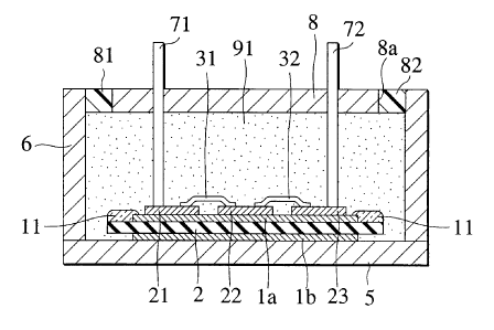
Fig. 1 is a cross sectional view showing a configuration of a package
for a semiconductor power device with the DBC substrate. In the package,
a plural of semiconductor chips 21, 22 and 23 are disposed on a copper film
1a that is attached on a top surface of an insulating A1N substrate 2 and
another copper film 1b that is attached at a bottom surface of an insulating
A1N substrate 2 except a peripheral region thereof. The semiconductor
chips 21, 22 and 23 are connected electrically with each other via lead wires
31 and 32 such as bonding wires and ribbon wires. These semiconductor
chips 21, 22 and 23 may, for example, include semiconductor power chips 21,
23 and a control circuitry chip 22 for controlling the semiconductor power
chips 21 and 23.
The copper film 1b bonded to the bottom surface of the AlN
substrate 2 is attached to the center of a metallic heat sink 5. A case (body
of a container) 6 is equipped on a peripheral region of the heat sink 5 to
surround the entire AlN substrate 2 as shown in Fig. 1.
A terminal holder 8 has external terminals (electrode terminals for
external connection) 71, 72 and an aperture 8a, and is fined at an upper
portion inside the case (container body) 6 in order to close the outer case 6.
The external terminals 71 and 72 are employed such members as to realize
electrical conduction to external from each of the semiconductor power chips
21, 23 and the control circuitry chip 22 inside the case (container body) 6.
A silicone gel 91 or an insulating material is flowed through the
aperture 8a into a module which is surrounded by the conductive bottom
plate 5 used as the heat sink, the case (container body) 6 and the terminal
holder 8. An epoxy resin is thereafter provided on the silicone gel to seal.
After sealing with the epoxy resin, arranging the terminal holder 8 to close
the case, which may consist 'of a material as same as or different from that
of the outer case, then closing the aperture 8a with sealing materials 81 and
82 after setting the silicone gel 91.
In the particular case where the IPM is used in a high voltage
power equipment, a hygroscopic property presented in the silicone gel 91
may degrade electric characteristics. Therefore, suitable adhering
methods and adhering structures, which can suppress generation of
2
CA 02255441 1998-12-07
openings and joints among the components by strong bonds between the
outer case 6 and the heat sink (the conductive bottom plate) and between
the lid (terminal holder) 8 and the epoxy resin, for example, are employed to
prevent humidity from penetrating into the IPM as far as possible. An
inner structure such as a space and a pressure-releasing valve is also
provided inside the IPM to prevent the silicone gel 91 from swelling and
exuding, and to reduce the heat stress applied to the epoxy resin.
The package structure shown in Fig. 1 may improve, by employing
a high heat conductive A1N substrate, a thermal conductivity between the
conductive bottom plate serving as the heat sink and the substrate, and
may also reduce the amount of a molybdenum (Mo) plate and a solder
material by bonding the semiconductor chip directly to the A1N substrate 2
that has the top copper film la. This is an advanced technology in the
radiation planning which can reduce the heat resistance and simplify the
structure as mentioned above.
However, the above-described conventional IPM has several
technical problems that are derived from the structure thereof. These
technical problems will be described below.
First, in order for undergoing to be used under a high voltage, the
IPM adopts the adhering method or the adhering structure that can
suppress the generation of the openings and joints between different
components by the strong bonds. This configuration may play the role of
reducing the moisture penetration. However, it is impossible to remove the
generation of the openings and joints completely, leaving a tiny opening or
joint within the semiconductor device. In addition, bonding the
components strongly may increase the heat stress in a portion where
different thermal expansion coefficients exist between components such as
the outer case 6 and the heat sink (conductive bottom plate) 5, and may
cause a breakage of the outer case 6 and an enlargement of the opening
remained. The breakage of the outer case 6 and the enlargement of the
opening may invite a moisture absorption by the silicone gel, resulting in a
cause to degrade electrical properties and durability thereof.
Second, adding a component such as the pressure-releasing valve
for relieving the heat stress inside the IPM may complicate an inner
structure of the device and increase a size of the entire device.
Third, since the conventional IPM is produced from several
3
CA 02255441 1998-12-07
materials such as the outer case 6, the lid (terminal holder) 8, the silicone
gel 91 and the epoxy resin, the heat stress may be generated due to the
differences among the thermal expansion coefficients of the materials, and a
complicated force is applied to each portion inside the device, resulting in
the breakage and the degradation of the substrate and electronic
components in the device. In general, the steps that are required for
assembling the device increases in accordance with the number of the
materials used, causing a reduction of reliability of the product and an
increase of cost.
Fourth, whereas the package structure of the conventional IPM has
the advantage for planning the heat radiation to realize a high breakdown
voltage, it leaves a problem with respect to the dielectric breakdown.
Namely, the package structure mentioned above employs the silicone gel 91
as the insulating material, but the silicone gel 91 has a property in which a
dielectric breakdown voltage is lower than those of general solid insulators.
Because a creeping distance between the silicone gel 91 and the A1N
substrate (a distance from an edge of the semiconductor power chip 21 or 23
to an edge of the A1N substrate 2) is short, a creeping breakdown at the
interface between the both may occur. The adhesion at the interface
between the both is insufficient, and a creeping discharge may occur easily.
Fifth, in the conventional semiconductor module, when the
insulating substrate that receives the semiconductor chip is located directly
on the bottom plate 5 of the metallic case (container body) that serves as the
heat sink, the dielectric breakdown at the interface between the insulating
substrate and the silicone gel may occur easily, because the creeping
distance is short and the metallic bottom plate serves as a back electrode
during the creeping discharge, extending the creeping discharge with ease.
Such the creeping breakdown and the creeping discharge do not
occur when driven under a rated voltage, but are considered to occur during
driven under a higher voltage than the rated voltage. Once the creeping
breakdown or discharge occurs, the dielectric breakdown voltage is lowered
and the dielectric breakdown may be easily caused.
In view of increasing the breakdown voltage and improving the
reliability, therefore, suppressing the creeping breakdown and discharge to
prevent the dielectric breakdown is required.
4
CA 02255441 1998-12-07
SUMMARY OF THE INVENTION
The present invention is made in consideration of the above
problems, and has an object to provide a package for a semiconductor power
device with a high reliability.
Another object of the present invention is to provide a package for a
semiconductor power device capable of preventing the dielectric breakdown,
increasing the breakdown voltage and improving the reliability.
A different object of the present invention is to provide a package
for a semiconductor power device capable of preventing damages to the
module and operation defects in the semiconductor chip caused by the heat
stress applied to the semiconductor chip and the containing case (container
body) due to the thermal expansion and the thermal shrinkage of a filling
agent.
A further object of the present invention is to provide a package for
a semiconductor power device capable of providing a sufficient waterproof
effect to the semiconductor module.
A further different object of the present invention is to provide a
package for a semiconductor power device having an advanced electric
property and a high durability.
A further object of the present invention is to provide a method for
assembling a package for a semiconductor power device having an advanced
electric property and a high durability.
An essential point of a first and a second features of the present
invention is to realize a higher breakdown voltage of the package for the
semiconductor power device, which is achieved with a configuration that
can suppress the creeping breakdown and the creeping discharge at an
interface of two kinds of insulating materials or the DBC substrate and the
silicone gel.
In order to suppress the creeping breakdown and the creeping
discharge at the interface of the two kinds of insulating materials, a system
for increasing the breakdown voltage by interposing an insulating resin
such as an epoxy resin and a polyester resin which has a dielectric
breakdown voltage higher than those of both the insulating materials
therebetween (the first feature), and a system for relieving the electric
field
5
CA 02255441 1998-12-07
across the interface between the insulating materials (the first and second
features) are considered.
(a) The system for increasing the breakdown voltage according to
the first feature may also relax the electric field strength. Moreover, it is
particularly preferable to interpose a thicker insulator by heaping or
adhering a solid in view of suppressing a penetrative puncture.
(b) The system for relieving the electric field according to the fir st
and second features includes a material type which interposes an insulator
having a median permittivity of those of both the insulators therebetween,
and an engineering type which eliminates any sharp shapes such as corners
and rough surfaces that cause the creeping discharge at the interface
between both the insulating materials with ease.
(b-1) The following ways are available as the material
type:
a way for coating a resin such as the epoxy and polyester between
both the insulating substrates; and a way for further filling into
the resin a powdered ceramic such as an aluminum oxide
(hereinafter,
referred to as "A120s") and the A1N.
(b-2) The following ways are considered as the engineering
type: a way for contacting the copper film tightly with the A1N
substrate by covering all the edges and corners of the film with
the resin; and a way for polishing to smooth the surface of the
outer edge region of the DBC substrate.
On the basis of the above novel knowledge found experimentally by
the present inventors, the first feature of the present invention lies in a
package for a semiconductor power device which comprises at least: a
conductive bottom plate serving as a heat sink; an insulating substrate
mounted on the bottom plate; a conductive film formed on the insulating
substrate selectively to expose a peripheral region of the insulating
substrate and a semiconductor chip mounted on the conductive film; a
solidified insulating material disposed on an outer edge region of the
conductive film and the peripheral region of the insulating substrate; and
an insulating material formed on the semiconductor chip. "The solidified
insulating material" may, for example, a hardened resin.
6
CA 02255441 1998-12-07
According to the first feature of the present invention, the solidified
insulating material disposed on the outer edge region of the conductive film
and the peripheral region of the insulating substrate may contact the outer
edge region of the conductive film with the peripheral region of the
insulating substrate tightly. Further, the solidified insulating material
interposed into an interface between the both --the conductive film and the
peripheral region of the insulating substrate-- may relax an electric field
strength across the interface between the both and make it difficult to cause
the creeping discharge. As a result, the prevention of the dielectric
breakdown, the realization of a higher breakdown voltage of the
semiconductor power device and the improvement of the reliability can be
achieved. If a height of the solidified insulating material exceeds a
thickness of the semiconductor chip, the thick the solidified insulating
material can suppress a penetrative puncture in which the discharge
punches through the solidified insulating material from the outer edge
region of the conductive film, and can prevent the creeping breakdown
completely. Containing the powdered aluminum oxide in the solidified
insulating material may further relax the electric field strength and make it
difficult to cause the creeping breakdown.
In the first feature of the present invention, it is possible to further
comprise a container arranged on the bottom plate, surrounding the
insulating substrate; an upper lid arranged at an upper portion of the
container; an external terminal supported through the upper lid and
connected electrically with the semiconductor chip. Then the insulating
material can be filled within the container to cover the semiconductor chip.
The second feature of the present invention lies in a package for a
semiconductor power device which comprises at least: a conductive bottom
plate serving as a heat sink; an insulating substrate mounted on the bottom
plate, having a smooth region of a given surface roughness near a
peripheral region thereof; a conductive film formed selectively on the
insulating substrate, and a semiconductor chip mounted on the conductive
film; and an insulating material formed on the semiconductor chip.
According to the second feature of the present invention, an
exposed top surface at the peripheral region of the insulating substrate or a
bottom surface opposing to the top surface, that is, a plane mating to the
7
CA 02255441 1998-12-07
conductive bottom plate serving as the heat radiating plane has the smooth
region of the given surface roughness, which may not cause a partial
discharge from the surface at the peripheral region of the insulating
substrate. Thus, the prevention of the dielectric breakdown, the
realization of a higher breakdown voltage of the semiconductor power
device and the improvement of the reliability can be achieved.
The "given surface roughness" means a certain flatness realized by
polishing. For example, a surface roughness smaller than 0.05 ,u m, which
is at least one order smaller than the conventional roughness of the
insulating substrate may be preferable. A method for polishing to achieve
the "smooth region having the given surface roughness" is based practically
on the following experiments performed by the present inventors:
When causing the dielectric breakdown in the simple A1N by
means of a ball-plane electrode pair in an insulating liquid or a
perfluorocarbon (dielectric constant: 1.86), a breakdown position is located
at a portion slightly apart from a contacting portion with the ball;
When causing the dielectric breakdown at the AlN substrate in the
perfluorocarbon, a breakdown position is located at the edge of the copper
film, and a value of the dielectric breakdown voltage increases by about
10 %;
On the other hand, when causing the dielectric breakdown at the
A1N substrate in the silicone gel (dielectric constant: about 2.8), a
breakdown position is located at a portion apart from the edge of the copper
film, and the value of the dielectric breakdown voltage further increases by
about 10 %;
The dielectric breakdown in the perfluorocarbon left partial
discharge scars around the electrodes uniformly, while the dielectric
breakdown in the silicone gel left tree-like discharge scars locally; and
When causing the dielectric breakdown in the silicone gel after
polishing the surface of the AlN substrate outside the edge of the copper
film to the given surface roughness by 3 ,u m has further increased the
value of the dielectric breakdown voltage by about 10 % or more.
These results are observed similarly in insulating substrates other
than the A1N substrate, for example, an alumina (AlzOs) substrate and a
beryllia (Be02) substrate. The present inventors therefore conclude that
the number (area) of the partial discharge scars has a relationship
8
CA 02255441 1998-12-07
proportional to the value of the dielectric breakdown voltage, and that the
smoothness of the surface has a relationship proportional to the value of the
dielectric breakdown voltage. As the partial discharge may take place due
to the irregularity of the surface, and as the dielectric breakdown may occur
due to the partial discharge in the A1N substrate, the upper or bottom
surface of the peripheral region of the insulating substrate should be
completed so as to have the given surface roughness.
A solidified insulating material, or a hardened resin as similar as
that of the first feature may be applied on the smooth region of the
insulating substrate. Thus, the prevention of the dielectric breakdown, the
realization of the higher breakdown voltage of the semiconductor power
device and the improvement of the reliability can be achieved.
Similar to the first feature, in the second feature of the present
invention, it is possible to further comprises a container arranged on the
bottom plate, surrounding the insulating substrate; an upper lid arranged
at an upper portion of the container; an external terminal supported
through the upper lid and connected electrically with the semiconductor
chip. Then the insulating material can be filled within the container to
cover the semiconductor chip.
The third feature of the present invention lies in a package for a
semiconductor power device which comprises at least: a conductive bottom
plate serving as a heat sink, wherein the bottom plate has a notch arranged
in a peripheral region of a surface thereof; an insulating substrate mounted
on the bottom plate; a conductive film formed on the insulating substrate
selectively to expose a peripheral region of the insulating substrate and a
semiconductor chip mounted on the conductive film; and an insulating
material formed on the semiconductor chip.
According to the third feature of the present invention, a creeping
distance for a creeping current that is generated when flowing from the
semiconductor chip through the insulating substrate may be substantially
elongated, and the creeping breakdown voltage of the semiconductor power
device may be increased. The notch is preferably located outwardly apart
from a region for mounting the semiconductor chip. Thus, as the
insulating substrate below the region for mounting the semiconductor chip
9
CA 02255441 1998-12-07
can contact tightly at least with the heat sink, the then mal r adiation
effect
of the semiconductor chip can be maintained. If an insulating material
with a high thermal conductivity is buried within the notch, the notch
serves as an insulator. Therefore, the creeping breakdown voltage of the
semiconductor device can be further increased certainly, and the radiation
of the heat from the insulating substrate can be performed sufficiently.
Similar to the first and second features, it is possible to further
comprises a container arranged on the bottom plate, surrounding the
insulating substrate; an upper lid arranged at an upper portion of the
container; an external terminal supported through the upper lid and
connected electrically with the semiconductor chip. Then the insulating
material can be filled within the container to cover the semiconductor chip.
The fourth feature of the present invention lies in a package for a
semiconductor power device which comprises at least: a conductive bottom
plate serving as a heat sink; an insulating substrate mounted on the bottom
plate; a conductive film formed on the insulating substrate selectively to
expose a peripheral region of the insulating substrate and a semiconductor
chip mounted on the conductive film; a container arranged on the bottom
plate, surrounding the insulating substrate; an upper lid arranged at an
upper portion of the container; an inlet formed at a part of the upper lid; an
insulating material injected through the inlet to fill the container; and a
waterproof and flexible film located at and to close the inlet.
According to the fourth feature of the present invention, even if the
thermal expansion and shrinkage of the insulating material due to the
variation of temperature occur, the heat stress can be relaxed because of a
deformation of the flexible film which closes the inlet for injecting
insulating material. A metallic film may be employed as the film. A
multi-layer film which consists of stacked waterproof films and metallic
films may also be utilized. A mufti-layer structure which has a film in at
least one layer capable of adhering to a film-fixing plane around the inlet
for
insulating material with an adhesion higher than those of the other stacked
films may be applied to the flexible film to ensure tight contacts among the
films. A laminated film which has a waterproof film in at least one layer
and another film with a greater resistance against the heat stress compared
to that of the waterproof film in at least another layer may also be used as
CA 02255441 1998-12-07
the flexible film.
The fifth feature of the present invention lies in a package for a
semiconductor power device which comprises at least: a conductive bottom
plate serving as a heat sink; an insulating substrate mounted on the bottom
plate; a conductive film formed on the insulating substrate selectively to
expose a peripheral region of the insulating substrate and a semiconductor
chip mounted on the conductive film; an insulating material formed on the
semiconductor chip; and a foam provided on the insulating material.
According to the fifth feature of the present invention, as the foam
which is filled on the insulating material can serve as a buffer against the
thermal expansion and shrinkage of the insulating material such as the
silicone gel, the heat stress applied to the package for the semiconductor
power device may be relaxed.
Similar to the first to third features, it is possible to further
comprises a container arranged on the bottom plate. Then the insulating
material can be filled within the container up to a middle height; and the
foam is provided on the insulating material.
The sixth feature of the present invention lies in a package for a
semiconductor power device which comprises at least: a conductive bottom
plate serving as a heat sink; an insulating substrate mounted on the bottom
plate; a conductive film formed on the insulating substrate selectively to
expose 'a peripheral region of the insulating substrate and a semiconductor
chip mounted on the conductive film; a container arranged on the bottom
plate, surrounding the insulating substrate; a jog portion formed on a side
of an upper aperture of the container; a sealing material provided in the
aperture, having another jog portion corresponding to the jog portion of the
aperture; and an insulating material formed on the semiconductor chip to
fill the container.
According to the sixth feature of the present invention, presence of
the jog portion formed on the upper part of the container may elongate a
distance at an adhered interface between the container and the sealing
material. The adhered interface may substantially reduce an amount of
moisture that penetrates into the container through the interface, because
the amount is inversely proportional to the second power of the distance.
11
CA 02255441 1998-12-07
The seventh feature of the present invention lies in a package for a
semiconductor power device which comprises at least: a conductive bottom
plate serving as a heat sink; an insulating substrate mounted on the bottom
plate; a conductive film formed on the insulating substrate selectively to
expose a peripheral region of the insulating substrate, for mounting
semiconductor chip on the conductive film; a container arranged on the
bottom plate, surrounding the insulating substrate; an insulating material
formed on the semiconductor chip to fill the container; an upper lid
arranged at an upper portion of the container; an external terminal
supported through the upper lid and connected electrically with the
semiconductor chip; and an insulating sheath for covering an outer surface
of the external terminal.
According to the seventh feature of the present invention, even in a
structure where the external terminal passes through a material with a
relatively lower dielectric breakdown voltage such as the foam, the
dielectric breakdown voltage can be increased. The insulating sheath
which covers the external terminal passes through the upper lid and the
insulating material. The insulating sheath may, for example, be made of
resin. Therefore, if the dielectric constant of the sheath is lower than those
of the upper lid and the insulating material, an electric field near the
external terminal becomes greater than that when the external terminal is
not covered with the insulating sheath. Thus, a material which has a
dielectric constant higher than that of the upper lid is required as the
insulating sheath for covering. It is also required, of course, that the
dielectric constant of the insulating sheath for covering is higher than that
of the insulating material. Thus, the dielectric breakdown voltage between
the external terminals can be increased and the generation of the dielectric
breakdown can be prevented.
The eighth feature of the present invention lies in a package for a
semiconductor power device which comprises at least: a conductive bottom
plate serving as a heat sink; an insulating substrate mounted on the bottom
plate; a conductive film formed on the insulating substrate selectively to
expose a peripheral region of the insulating substrate and a semiconductor
chip mounted on the conductive film; a thermoplastic insulating resin
12
CA 02255441 1998-12-07
formed on the semiconductor chip; and an external terminal arranged
through the thermoplastic insulating resin and connected electrically with
the semiconductor chip.
According to the eighth feature of the present invention, as the
entire semiconductor chip is covered with the thermoplastic resin that has a
high waterproof property, the degradation of the semiconductor power
device due to the absorption of humidity can be prevented, and advanced
electric properties can be obtained. Further, an inner structure can be
simplified compared to the conventional one, the package for the
semiconductor power device can be miniaturized, and the steps required to
assemble the semiconductor power device can be reduced.
In the eighth feature of the present invention, the thermoplastic
insulating resin can seal the insulating substrate, the semiconductor chip
and at least a part of the bottom plate integrally. However, it is also
possible to implement a configuration, in which the thermoplastic resin is
molded only on the insulating substrate so as not to contact with the bottom
plate. By molding the thermoplastic resin only on the insulating substrate
without contacting to the bottom plate, a thickness of molding and an
amount of the thermoplastic resin used can be reduced. Further, as the
molding can be easily performed and the assembling time can be shortened,
the problems during molding such as the deformation of the components
which are employed to construct the device can be reduced, and the
durability and reliability of the package for the semiconductor power device
can be improved.
The ninth feature of the present invention lies in a method for
assembling a package for a semiconductor power device which comprises at
least the steps of: (a) bonding an insulating substrate on a conductive
bottom plate; (b) mounting a semiconductor chip on the insulating
substrate; (c) connecting electrically the semiconductor chip with an
external terminal; (d) injection-molding an insulating resin on the bottom
plate to form an outer case consisting of the insulating resin for surrounding
the insulating substrate and the semiconductor chip; and (e) filling a
insulating resin within the outer case.
According to the ninth feature of the present invention, the outer
case is produced by injecting the insulating resin onto the metallic base, so
13
CA 02255441 1998-12-07
the outer case and the metallic base are firmly integrated. In addition, the
adhesion between the outer case and the metallic base is improved, and the
moisture penetration into the device can be prevented. The insulating
resin may be a thermoplastic insulating resin or another resin.
A polyphenylene sulfide may be used as the thermoplastic resin in
the eighth and ninth features. Catalysts, additives and inorganic fillers
may also be employed suitably to adjust the adhesion and to relax the inner
stress with using the polyphenylene sulfide as a main constituent.
Preferable examples of the inorganic fillers may include a fused silica, a
powdered quartz, a powdered glass, a short glass fiber, an alumina (Al2Os)
and an aluminum nitride (A1N). In the case where the thermoplastic resin
has a two-layer structure, a sandwich-molding may be applied to mold the
resin. A vacuum pressure impregnation treatment may also be employed
preferably for impregnating the insulating resin into the insulating
substrate in advance to improve an insulating property of the insulating
substrate by repairing the inner defects of the insulating substrate. A
laminated structure that consists of plural insulating substrate materials
may be applied to the insulating substrate to improve the insulating
property of the insulating substrate.
The "semiconductor power devices" in the first through ninth
features may include various power devices such as the IGBT, the Power
MOSFET, the Power BJT, a Power Static Induction Transistor (SIT), a
Thyristor, the GTO Thyristor and a Static Induction (SI) Thyristor. The
"semiconductor chips" means such semiconductor chips that have at least
one of the semiconductor power devices mounted thereon. These
semiconductor chips may also include a chip which has a circuit for
controlling the semiconductor power device and a protection circuit
mounted thereon. A power IC that integrates the control circuit on the
same monolithic substrate where the semiconductor power device is formed
may also be employed. At least one of these "semiconductor chips" may be
disposed on the conductive film. The package for semiconductor power
device according to the present invention can include various electronic
components, for example, resistors, capacitors, inductors, circuit wires and
leads such as bonding wires.
14
CA 02255441 1998-12-07
Other and further objects and features of the present invention will
become obvious upon an understanding of the illustrative embodiments
about to be described in connection with the accompanying drawings or will
be indicated in the appended claims, and various advantages not referred to
herein will occur to one skilled in the art upon employing of the invention in
practice.
BRIEF DESCRIPTION OF THE DRAWINGS
Fig. 1 is a cross sectional view showing a conventional package
structure for a semiconductor power device;
Fig. 2A, 2B are cross sectional views showing a package structure for
a semiconductor power device according to a first embodiment of the present
invention;
Fig. 3A is a plan view showing still another package structure for a
semiconductor power device according to a modification (MODIFICATION
1) of the first embodiment of the present invention;
Fig. 3B is a step cross sectional view taken along the line III B-III B
of Fig. 3A;
Fig. 4A is a cross sectional view showing a still another package
structure for a semiconductor power device according to another
modification (MODIFICATION 2) of the first embodiment of the present
invention;
Fig. 4B is a cross sectional view showing a still another package
structure for a semiconductor power device according to still another
modification (MODIFICATION 3) of the first embodiment of the present
invention;
Fig. 5 is a cross sectional view showing a package structure for a
semiconductor power device according to a second embodiment of the
present invention;
Fig. 6 is a cross sectional view showing a package structure for a
semiconductor power device according to a third embodiment of the present
invention;
Fig. 7 is a cross sectional view showing a package structure for a
semiconductor power device according to a fourth embodiment of the
present invention;
CA 02255441 2002-07-05
''~
Fig. $ is a cross sectional view showing a package structure for a
semiconductor power device according to a fifth embodiment of the present
invention;
Fig. 9 is a cross sectional view showing a package structure for a
semiconductor power device according to a sixth embodiment of the pr esent
invention;
Fig. 10 is a longitudinal cross sectional view showing a package
structure for a semiconductor power device according to a seventh
embodiment of the present invention;
Fig. 11 is a longitudinal cross sectional view showing a structure
of a package for a semiconductor power device according to an eighth
embodiment of the present invention;
Fig. 12 is a diagram showing a result of a breakdown voltage test
for the package for semiconductor device according to the eighth
embodiment in comparison with a result of the prior art;
Fig. 13A is a longitudinal cross sectional view showing a package
structure for a semiconductor power device according to a modification
(MODIFICATION 1) of the eighth embodiment of the present invention;
Fig: 13B is a longitudinal cross sectional view showing a package
structure for a semiconductor power device according to another
modification (MODIFICATION 2) of the eighth embodiment of the present
invention;
Fig. 14A is a longitudinal cross sectional view showing a package
structure for a semiconductor power device according to a different
modification (MODIFICATION 3) of the eighth embodiment of the present
invention;
Fig. 14B is a longitudinal cross sectional view showing a package
structure for a semiconductor povwer device according to a further different
modification (MODIFICATION 4) of the eighth embodiment of the present
invention;
Fig. 14C is a longitudinal cross sectional view showing a package
structure for a semiconductor power device according to a further
modification (MODIFICATION 5) of the eighth embodiment of the present
invention;
Fig. 15 is a longitudinal cro s sectional view showing a package
structure for a semiconductor power device according o a further
16
CA 02255441 2002-07-05
°~
modification (MODIFICATIO1~T 6) of the eighth embodiment of the present
invention;
Fig. 16A is a longitudinal cross sectional view showing a package
structure for a semiconductor power device according to a further
modification (MODIFICATION 7) of he eighth embodiment of the present
invention;
Fig. 16B is a longitudinal cross sectional view showing a package
structure for a semiconductor power device according to a further
modification (MODIFICATION 8) of the eighth embodiment of the present
invention;
Fig. 17A is a longitudinal cross sectional view showing a package
structure for a ~ semiconductor power device according to a ninth
embodiment of the present invention;
Fig. 17B is a partially expanded longitudinal cross sectional view
showing a package structure for a semiconductor power device according to
a modification of the ninth embodiment of the present invention;
Fig. 18 is a diagram showing a.variation of remnant stress in a
thermoplastic resin in response to a variation of an angle at a molded side of
the thermoplastic resin in the package structure for semiconductor power
device according to the ninth embodiment of the present invention;
Fig. i9 is a longitudinal cross sectional view showing a package
structure for a semiconductor power device according to a tenth
embodiment of the' present invention; and
Figs. ~20A to 20D are cross sectional process views
showing a method for manufacturing the semiconductor device according to
the tenth embodiment of the present invention.
DETAILED DESCRIPTION OF THE PR~EFER.R,ED EMBODIMENTS
Various embodiments of the present invention will be described
with reference to the accompanied drawings. It is to be noted that the
same or similar reference numerals are applied to the same or similar parts
and elements throughout the drawings, and the description of the same or
similar parts and elements will be omitted or simplified. Generally and as
it is conventional in the representation of semiconductor devices, it will be
appreciated that the various drawings are not drawn to scale from one
T7
CA 02255441 1998-12-07
figure to another nor inside a given figure, and in particular that the layer
thicknesses are arbitrarily drawn for facilitating the reading of the
drawings.
(FIRST EMBODIMENT)
Fig. 2A is a cross sectional view showing a structure of a package
for a semiconductor power device according to a first embodiment of the
present invention. The first embodiment of the present invention intends
to improve the reliability by preventing the creeping breakdown and the
creeping discharge between an insulating substrate (ceramic substrate) 2
and an adjacent silicone gel 91. Whereas an aluminum nitride (A1N), an
alumina (AlzOs), and a beryllium oxide such as a beryllia (Be02) can be used
as the insulating substrate (ceramic substrate) 2, the following description
will be made with respect to an A1N substrate. In a practical use, the A1N
substrate 2 is provided with a top copper film 1a and a bottom copper film
1b both attached on a top surface and under a bottom surface of the AlN
substrate 2, respectively, except peripheral regions thereof by the direct
bond copper (DBC) technique. The top copper film 1a on the A1N substrate
2 is constructed in the form of a certain inner pattern. On such the top
copper film 1a, semiconductor power chips 21, 23 and a control circuitry
chip 22 merging control circuitry to control them are disposed.
The insulating substrate 2 on which the semiconductor chips 21, 22
and 23 are mounted is contained in a case 6 (container body). A bottom
plate of the case 6 (container body) to which the bottom copper film 1b is
attached is made of a metal to serve as a heat sink 5. Bonding wires 31
and 32 are connected with the semiconductor power chips 21 and 23 on the
insulating substrate, from which external terminals (lead wires) 71 and 72
are drawn out from the case (container body) in order to make electrical
connections with outside a module. The external terminals 71 and 72 are
used for supplying power to the semiconductor power chips 21, 23 and the
control circuitry chip 22. The silicone gel 91 or an insulating material is
filled within the case 6 (container body) to protect the connecting leads 31
and 32. A top surface of the case 6 (container body) is provided with a
terminal holder 8 or an upper lid. An inlet for injecting the insulating
material (an inlet for injecting the silicone gel) is generally sealed with
resinous sealing materials 81 and 82. The entire semiconductor device has,
18
CA 02255441 1998-12-07
for example, an outer size of about 100 mm X 70 mm X 10 mm.
Various power devices such as IGBTs, power MOSFETs, power
BJTs, power SITs, thyristors, GTO thyristors or SI thyristors can be used as
the semiconductor power chips 21 and 23. An n-MOS control circuit, a p-
MOS control circuit, a CMOS control circuit, a bipolar control circuit, a Bi-
CMOS control circuit and a SIT control circuit can be used as the control
circuitry. These control circuits may contain an overvoltage protection
circuit, an overcurrent protection circuit and an overheat protection circuit.
The semiconductor power chips 21, 23 and the control circuitry chip 22 are
electrically connected with each other through the connecting leads 31 and
32. Bonding wires or bonding strips made of gold (Au), copper (Cu),
aluminum (Al) and the like may be used as the connecting leads 31 and 32.
Besides the semiconductor power chips 21, 23 and the control circuitry chip
22, various electronic components such as resistors, condensers, coils and
the like, and also a circuit such as a power supply can be provided in the
package of the semiconductor power device according to the first
embodiment of the present invention.
As shown in Fig. 2A, an upper portion of the peripheral region of
the A1N substrate 2 and an edge portion (outer edge region) of the copper
film facing thereto are coated with a solidified insulating material, or a
hardened resin 11. Resins which have a breakdown voltage higher than
that of the silicone gel 91 and a good adhesion to the A1N substrate 2 are
desirable for the solidified insulating material 11. For example, an epoxy
resin is used herein as the solidified insulating material 11. A polyester
resin may also be used as the solidified insulating material 11.
A thickness of the solidified insulating material 11 relates to a
creeping distance from the semiconductor power chips 21 and 23 to the edge
of the A1N substrate 2. A long creeping distance may effect to prevent the
breakdown even if the resin is thin. In Fig. 2A, the shoulder of the outer
edge of the top copper film 1a is fully coated with the solidified insulating
material 11, but the shoulder of the top copper film 1a is not always needed
to be fully coated with the solidified insulating material 11. However the
effectiveness of the first embodiment of the present invention to suppress
the creeping discharge is accomplished to some extent in the case that the
corner part formed between the edge wall of the top copper film la and the
A1N substrate 2 is buried with the resin 11 as shown in Fig. 2B. By the
19
CA 02255441 1998-12-07
configuration as shown in Fig. 2B, in which the shoulder of the outer edge of
the top copper film la is exposed, the amount of resin 11 employed is saved,
and results in reducing the manufacturing cost of the package. If the
creeping distance is substantially the same as the thickness of the A1N
substrate 2, a further improvement of the preventing effect is obtained by a
structure which piles up the resin 11.
It is preferable that the solidified insulating material 11 is not be
coated on the conductive bottom plate 5 that serves as the heat sink. If the
solidified insulating material (the resin) 11 is coated and fixed on the
conductive bottom plate 5 that serves as the heat sink, there may be
introduced a counter result that causes peeling off of the resin 11 by heat
cycles due to a mismatching in thermal expansion coefficients of the A1N
substrate vs. the conductive bottom plate 5, and resulting in the creeping
breakdown with ease.
As mentioned above, the outer edge region of the top copper film la
and the peripheral region of the A1N substrate 2 are adhered tightly
because the solidified resin 11 is provided on the outer edge region of the
top
copper film la and the periphery region of the A1N substrate 2. Further,
existence of the resin 11 at an interface between the outer edge region of the
top copper film la and the peripheral region of the A1N substrate 2 can relax
an electric field strength at the interface between the both, and can prevent
the creeping discharge. Therefore, the prevention of the dielectric
breakdown, the improvement of the reliability and the increase of the
breakdown voltage can be realized. The solidified resin 11 provided on the
outer edge region of the top copper film la and the peripheral region of the
A1N substrate 2 may act as a reinforcement member. Hence, a
miniaturization of the DBC substrate can be expected because of the
improvement of the reliability in the junction between the top copper film
1a and the AlN substrate 2 along with the improvement of the mechanical
strength of the A1N substrate 2.
MODIFICATION OF FIRST EMBODIMENT:
MODIFICATION 1: In Fig. 2A, only the peripheral of the entire
outer edge region of the top copper film la is coated with the solidified
insulating material 11, not only the edges facing to the peripheral region of
the A1N substrate 2, but also other edges of wiring patterns lc, 1d and 1e
consisting of the top copper film, for example, may also be coated with the
CA 02255441 1998-12-07
solidified insulating material 11 as shown in Figs. 3A and 3B. Fig. 3A is a
plan view showing a package structure for a semiconductor power device
according to a modification (MODIFICATION 1) of the first embodiment of
the present invention, and Fig. 3B is a step cross sectional view taken along
the line III B-III B of Fig. 3A. As shown in Fig. 3B, the DBC substrate is
provided with top copper films lc, 1d and 1e and a bottom copper film 1b
both attached on a top surface and under a bottom surface of the A1N
substrate 2, respectively, except peripheral regions. The top copper film on
the A1N substrate 2 is delineated into three inner patterns lc, 1d and 1e.
On such the top copper film 1d, semiconductor power device (IGBT)chips 24,
and two diode chips 25 and 26 are disposed. The inner patterns 1c and 1e
are serving as electrode terminals. The upper part of the inner patterns 1e
and IGBT chip 24 are electrically connected by bonding wires 34, 35, 36 and
37. And the lower part of the inner patterns 1e and IGBT chip 24 are
electrically connected by bonding wires 38, 39, 40 and 41. Further, the
inner patterns lc and IGBT chip 24 are electrically connected by a bonding
wire 33. As shown in Figs. 3A and 3B, by coating and coagulating with the
resin 11 which have a breakdown voltage higher than that of the silicone gel
the dielectric breakdown is further suppressed. A configuration to coat and
solidify only corners of the top copper film, that is generally square shape,
with the resin, may suppress the dielectric breakdown in some extent.
MODIFICATION 2: If the creeping breakdown voltage at the
interface between the AlN substrate 2 and the solidified insulating material
11 increases in the structure shown in Fig. 4A, the solidified insulating
material 11 may undergo a penetrative puncture at the peripheral region of
the top copper film la, and the creeping discharge may develop at the
interface between the solidified insulating material 11 and the silicone gel
91. The present modification (MODIFICATION 2) intends to suppress the
penetrative puncture in which the discharge punches through the solidified
insulating material 11 at the outer edge region of the copper film. In
particular, a thick solidified insulating material 12, or a thick resin 12
heaped up to a height that exceeds at least a thickness of the semiconductor
chip is used as shown in Fig. 4A instead of the solidified insulating material
(the resin) 11. According to the structure shown in Fig. 4A, the thick resin
12 prevent the penetrative puncture which punches through the resin 12 at
the outer edge region of the top copper film la, the creeping breakdown can
21
CA 02255441 1998-12-07
be prevented completely, in addition to the effectiveness described with
reference to Fig. 4A.
MODIFICATION 3: The epoxy resin 12 has a variety of viscosity.
Among those, the one with a lower viscosity makes it difficult to form the
heaped portion in the MODIFICATION 2 shown in Fig. 4A. A still another
modification (MODIFICATION 3) of the first embodiment of the present
invention intends to propose a structure which may form the heaped portion
easily. In the MODIFICATION 3, a heaped member 13 that is included
and mounted with the resin 11 is provided as shown in Fig. 4B. According
to such the configuration, as the heaped member 13 may be formed in
advance and thereafter it may be adhered with the resin 11 to form a
heaped shape easily, the solidified insulating material can be formed in a
thick shape easily, in addition to the effectiveness of the MODIFICATION 2.
The heaped member 13 may also be produced from an A1N, the same
material as that of the A1N substrate 2 instead of the resin. In the case
where the heaped member 13 consists of the AIN, in addition to the
effectiveness of the present embodiment, the reduction of the electric field
at
the edges of the top copper film la and the increase of the dielectric
breakdown voltage may be realized. Thus, the prevention of the dielectric
breakdown, the realization of the high breakdown voltage and the
improvement of the reliability can be achieved.
OTHER MODIFICATIONS: In the first embodiment, the
solidified insulating material, or the hardened epoxy resin can be disposed
on the edges of the semiconductor power chips 21 and 23 in the structures
shown in Figs. 2A-4B to further relax the electric field strength. The epoxy
resin has a dielectric constant ranging between 3.5-5.0, and has an
intermediate value between the dielectric constant of the A1N, about 8.8,
and that of the silicone gel 91, about 2.8. Therefore, coating the epoxy
resin that has the intermediate dielectric constant between those of the A1N
substrate 2 and the silicone gel 91 may relax the electric field strength at
the edge of the top copper film la. A powdered A120s may also be contained
in the resins 11-13 shown in Figs. 2A-4B in order to further relax the
electric field strength. The A120s has a dielectric constant of about 8.3.
Therefore, filling the powdered A120s into the heaped member 13, which is
made of a resin, or the resins 11 and 12 may further relax the electric field
strength and make it difficult to cause the creeping discharge. A powdered
22
CA 02255441 1998-12-07
A1N may be filled instead of the Al2Os. The powdered A120s and A1N may
also be filled together.
(SECOND EMBODIMENT)
Fig. 5 is a cross sectional view showing a structure of a package for
a semiconductor power device according to a second embodiment of the
present invention. The second embodiment of the present invention
intends of prevent the creeping breakdown and the creeping discharge in a
manner different from the first embodiment.
The package for a semiconductor power device according to the
second embodiment of the present invention employs an A1N substrate 2
that includes a top copper film la and a bottom copper film 1b disposed on a
top and under a bottom surfaces of the A1N substrate 2, respectively, except
the peripheral region by the DBC technique as same as the first
embodiment. The top copper film la on the A1N substrate 2 is delineated
and constructed in the form of a given inner pattern. The semiconductor
power chips 21, 23 and the control circuitry chip 22 merging control
circuitry for controlling these semiconductor power chips are mounted on
the top copper film 1a.
Various power devices such as IGBTs, Power MOSFETs and Power
BJTs may be used as the semiconductor power chips 21 and 23. Various
control circuits such as a CMOS control circuit, Bipolar control circuit and
BiCMOS can be employed as the control circuit. These control circuits may
contain an overvoltage protection circuit, an overcurrent protection circuit
and an overheat protection circuit. The semiconductor power chips 21 and
23 are connected electrically with the control circuitry chip 22 to each other
via bonding wires 31 and 32.
The insulating substrate 2 that mounts the semiconductor chips 21,
22 and 23 thereon is accomodated within a case 6 (container body). The
bottom plate, to which the bottom copper film 1b is attached, of the case
(container body) 6 serves as a heat sink 5 made of a metal. External
terminals (lead wires) 71 and 72 are drawn out of the case (container body)
for making electrical connections with the external of the module from the
semiconductor power chips 21 and 23 on the insulating substrate which are
connected to control circuitry chip 22 through the bonding wires 31 and 32.
The external terminals 71 and 72 are such terminals that supply power to
23
CA 02255441 1998-12-07
the semiconductor power chips 21, 23 and control circuitry chip 22. A
silicone gel 91 is filed within the case (container body) 6 to protect the
bonding wires 31 and 32. A top surface of the case (container body) 6 is
covered with a terminal holder 8. An inlet for injecting the silicone gel is
generally sealed with resinous sealing materials 81 and 82. Various
electronic components such as condensers and coils may be mounted on the
A1N substrate.
The package for semiconductor power device according to the
second embodiment of the present invention adopts such a structure that an
exposed top surface of the peripheral region in the A1N substrate 2 is
polished to make a smooth region 2a having a given surface roughness. In
general, the surface roughness of the insulating substrate employed in the
package for the semiconductor power device is 0.4-0.6 a m. However, the
given surface roughness of the smooth region 2a of the A1N substrate 2 in
the second embodiment is smaller than 0.05 a m, which is at least one order
smaller than the conventional roughness of the insulating substrate. And
it is preferable to polish the smooth region 2a to obtain a mirror like
surface.
If we use a SiC abrasive paper of #1000 mesh, it is easy to obtain the given
surface roughness at the smooth region 2a of the AlN substrate 2 in the
second embodiment. The mirror like polished finish is obtained by buffing.
Here, the smooth region 2a of the A1N substrate 2 is located
outwardly apart from the edge of the top copper film la. The polishing is
performed so as not to generate any gaps between the top copper film la
and the A1N substrate 2. Polishing the substrate over the top copper film
la may realize a greater effect if the top copper film la is still firmly
attached to the AlN substrate 2 without gaps.
According to the above configuration, the exposed surface of the
peripheral region of the AlN substrate 1 consists of the smooth region 2a
that is polished and has no surface roughness nor flatness defect. Thus,
the creeping discharge from the peripheral region surface of the A1N
substrate 2 may be prevented, and the breakdown voltage may be increased.
Therefore, it is possible to prevent the dielectric breakdown, to realize the
high breakdown voltage, and to improve the reliability.
COMBINATION OF SECOND WITH FIRST EMBODIMENTS:
The first embodiment shown in Figs. 2A-4B may be combined with
the second embodiment. Combined structures that apply the smooth
24
CA 02255441 1998-12-07
region 2a shown in Fig. 5 to the structures having the solidified insulating
material, or the resin 11 shown in Fig. 4A, the thick resin 12 shown in Fig.
4A and the resin 11 with the heaped member 13 shown in Fig. 4B are
desirable. According to these structures, both the advantages from the
first and second embodiments are obtained at the same time. Coating the
resins 11 and 12 over the smooth region 2a may increase the adhesion
among the resins 11, 12 and the AlN substrate 2 and the improvement of
the reliability to be expected.
MODIFICATION OF SECOND EMBODIMENT:
To further relax the electric field strength, the solidified insulating
material, or the hardened epoxy resin can be provided on the edges of the
semiconductor power chips 21, 23 and the control circuitry chip 22 in the
structure of the second embodiment or in the structure in combination of
the second and first embodiments. If the epoxy resin that has the
intermediate dielectric constant between those of the A1N substrate 2 and
the silicone gel 91 is coated on the edges of the semiconductor power chips
21 and 23, the electric field at the edge of the top copper film la can be
relaxed. Containing the powdered A120s (dielectric constant: about 8.3) in
the resins 11-13 may further relax the electric filed and prevent the
creeping discharge. The A1N powders may be filled instead of the AlzOs.
Both the A120a and A1N powders may also be filled together.
(THIRD EMBODIMENT)
Fig. 6 is a cross sectional view showing a structure of a package for
semiconductor power device according to a third embodiment of the present
invention. The third embodiment adopts a structure that has a polished
smooth region 2b at a bottom surface of an A1N substrate 2, which faces to a
conductive bottom plate 5 serving as a heat sink and also opposes to an
exposed top surface of a peripheral region of the A1N substrate 2 as shown
in Fig. 6, instead of the smooth region 2a at the exposed top surface of the
A1N substrate 2 in the second embodiment.
Similar to the second embodiment, the package for a semiconductor
power device according to the third embodiment of the present invention
employs the A1N substrate 2 that includes a top copper film la and a bottom
copper film 1b disposed on a top and under a bottom surfaces of the A1N
substr ate 2, respectively, except the peripheral region by the DBC technique
CA 02255441 1998-12-07
as same as the first embodiment. The top copper film la on the AlN
substrate 2 is delineated to form a given inner pattern. The semiconductor
power chips 21, 23 and the control circuitry chip 22 are mounted on the top
copper film la. The semiconductor power chips 21 and 23 are connected
electrically with the control circuitry chip 22 to each other via bonding
wires
31 and 32.
The insulating substrate 2 that mounts the semiconductor chips 21,
22 and 23 thereon is contained within a case 6. The bottom plate, to which
the bottom copper film 1b is attached, of the case 6 serves as a heat sink 5
made of a metal. External terminals 71 and 72 are drawn out of the case
for making electrical connections with the external of the module from the
semiconductor power chips 21 and 23 on the insulating substrate which are
connected to control circuitry chip 22 through the bonding wires 31 and 32.
The external terminals 71 and 72 are such terminals that supply power to
the semiconductor power chips 21, 23 and control circuitry chip 22. A
silicone gel 91 is filed within the case 6 to protect the bonding wires 31 and
32. A top surface of the case 6 is covered with a terminal holder 8. An
inlet for injecting the silicone gel is generally sealed with resinous sealing
materials 81 and 82.
The package for semiconductor power device according to the third
embodiment of the present invention adopts such a structure that an
exposed bottom surface of the peripheral region in the A1N substrate 2 is
polished to make a smooth region 2b having a given surface roughness.
The given surface roughness of the smooth region 2b of the A1N substrate 2
in the third embodiment is smaller than 0.05 a m, which is at least one
order smaller than the conventional roughness of the insulating substrate.
And it is preferable to polish the smooth region 2b to obtain a mirror like
surface. Although a taper is shown to clearly point out the smooth region
2b of the A1N substrate 2, it must be noted that the taper is not required in
the third embodiment, since the taper at the smooth region 2b does not
relate to the electric field, on the contrary to the top surface of the A1N
substrate 2.
The breakdown voltage slightly increases in the third embodiment.
The advantages by the polishing are slightly reduced compared to the
second embodiment where the exposed top surface of the peripheral region
of the A1N substrate 2 is polished. However, the package still have the
26
CA 02255441 1998-12-07
effectiveness in some extent, and further has an advantage not to require a
distinction of the top and bottom surfaces of the AlN substrate 2. The
peripheral region of the A1N substrate 2 is not restricted in the
configurations shown in Figs. 5 and 6, and the smooth region 2a of the
exposed top surface and the bottom smooth region 2b can be provided at the
same time.
COMBINATION OF THIRD WITH FIRST EMBODIMENT:
Combining the structure shown in Fig. 6 with any one of the
structures shown in Figs. 2A-4B with the solidified insulating materials
allows for obtaining the advantages from each the structure at the same
time. Further, combining the structure that realizes the both structures
shown in Figs.5 and 6, which has both polished surfaces 2a and 2b, with any
one of the structures shown in Figs. 2A-4B may also allow for obtaining the
respective effectiveness from each of the structures stated in the second and
third embodiments as well as the effectiveness in the structures shown in
Figs. 2A-4B, at the same time.
(FOURTH EMBODIMENT)
Fig. 7 is a cross sectional view showing a structure of a package for
a semiconductor power device according to a fourth embodiment of the
present invention. The package according to the fourth embodiment of the
present invention employs, as an insulating substrate (ceramic substrate) 2,
an A1N substrate that has a conductive film 1 such as copper film, or a
composite film comprising gold (Au) and nickel (Ni) films, disposed on a top
surface except a peripheral region thereof as shown in Fig. 7. In Fig. 7,
though the bottom conductive film is omitted, such bottom conductive film
can be attached at the bottom of the insulating substrate 2 as shown in the
first to third embodiments employing the DBC substrate. Semiconductor
power chips 21, 23 and a control circuitry chip 22 for containing control
circuitry for controlling these semiconductor power chips are disposed and
fixed tightly on the conductive film 1. Various power devices such as the
IGBT, the power MOSFET and the power BJT may be used as the
semiconductor power chips 21 and 23. The control circuitry may include
various control circuits such the CMOS control circuit, the bipolar control
circuit and the BiCMOS control circuit. These control circuits may contain
other circuits such as the overvoltage protection circuit and the overheat
27
CA 02255441 1998-12-07
protection circuit. The semiconductor power chips 21 and 23 are connected
electrically with the control circuitry chip 22 via bonding wires 31 and 32.
Further, as shown in Fig. 7, external terminals 71 and 72 are provided in
the package. The external terminals 71 and 72 are such terminals that
supply power to the semiconductor power chips 21, 23 and the control
circuitry chip 22. Various electronic components including passive
elements such as condensers and coils may also be contained in the
package.
The insulating substrate 2 on which the semiconductor chips 21, 22
and 23 are mounted is accommodated within a case (container body) 6. A
bottom plate of the case to which the insulating substrate 2 is attached
serves as a heat sink 5 made of a metal. A silicone gel 91 or an insulating
resin is filled within the case (container body) 6 to protect the bonding
wires
31 and 32. A top surface of the case (container body) 6 is covered with an
upper lid (terminal holder) 8. An inlet for injecting insulating material
(inlet for injecting the silicone gel) is generally sealed with resinous
sealing
materials 81 and 82.
The feature in the structure of the package for semiconductor
power device according to the fourth embodiment is characterized in that: a
notch or a groove is formed in a part of the conductive bottom plate 5 that
serves as the heat sink, which contacts with a bottom surface of the
insulating substrate 2 on which the semiconductor chips 21, 22 and 23 are
mounted. And a high heat conductive insulating resin 92 is embedded in
the notch (groove).
In general, the creeping discharge caused in one surface of the
insulating substrate may develop easily when another surface of the
substrate consists of a conductor. Therefore, digging a grooved portion
(notched portion), at the peripheral region of the insulating substrate 2, at
the surface of and in the metallic heat sink 5 and filling the grooved portion
(notched portion) with the insulating resin 92 as shown in Fig. 7 can
pr event the development of the discharge. In addition, by digging the
grooved portion (notched portion), the creeping distance may be extended,
and the creeping breakdown voltage can be increased.
A larger depth of the notched portion is desired to extend the
creeping distance as long as the conductive bottom plate 5 serving as the
heat sink can suffer to be used. The creeping breakdown voltage that folds
28
CA 02255441 1998-12-07
back around the insulating substrate 2 from the semiconductor chips 21 and
23 is desired to be higher than the creeping breakdown voltage that ravels
through the edge of the insulating substrate 2 from the semiconductor chips
21, 22 and 23 and reaches directly to the buried resin 92 and further
penetrates through the buried resin 92.
A start position of the notched portion that is formed in the
conductive bottom plate 5 or the heat sink is desirable to be located
outwardly apart from the peripheral of the semiconductor chips 21, 22 and
23. If the notch portion is formed directly beneath the semiconductor chips
21, 22 and 23, the thermal conduction and heat radiation effects from the
semiconductor chips 21, 22 and 23 will be insufficient.
The insulating substrate 2 generally used is mostly thin so as to
increase the thermal conduction and heat radiation effects and to reduce the
cost. Therefore, it is preferable to form the notched portion outwardly at
least from the edges of the semiconductor chips 21, 22 and 23 in order to
avoid the penetrative puncture in the insulating substrate 2 due to the
concentration of the electric field.
Injecting filling materials such as the silicone gel and other
insulating resins into the notched portion that is formed in the conductive
bottom plate or the heat sink can achieve the effectiveness to prevent the
creeping breakdown. Injecting the high heat conductive insulating resin
92 into the notched portion can also realize the good thermal conduction and
heat dissipation effects as mentioned above. An insulating resin that is
mixed with a high heat conductive material may also be employed instead
of the high heat conductive insulating resin 92. It is also desirable to
contact the injected resin tightly with the insulating substrate 2 without
making any openings between the resin and the notched portion in order to
obtain the good thermal radiation effect.
Whereas the surface of the high heat conductive insulating resin 92
injected into the notched portion is flattened as shown in Fig. 7, the high
heat conductive insulating resin 92 can be heaped up to a position
corresponding to the top surface of the insulating substrate 2. Burying a
resin with a resistivity smaller than that of the insulating substrate 2 or a
semi-conducting resin into the notched portion may also relax the electric
field strength. The geometrical start position to be notched, or the
shoulder of the groove may be made roundly. A cross sectional shape of the
29
CA 02255441 1998-12-07
notched portion (grooved portion) is not restricted to a rectangle shape, but
can be various shapes such as a mesa shape and a triangle shape.
(FIFTH EMBODIMENT)
Fig. 8 is a cross sectional view showing a structure of a package for
a semiconductor power device (semiconductor module) according to a fifth
embodiment of the present invention. An essential configuration of the
semiconductor module according to the fifth embodiment is mostly similar
with the semiconductor module already explained in the fourth embodiment,
so the duplicated items between them are omitted to explain. The feature
of the present semiconductor module is characterized in that an inlet for
injecting insulating material (inlet for injecting the silicone gel), which is
located at outside an upper lid (terminal holder) in an inner portion of a
case (container body) 6, is sealed with a flexible and waterproof film 14 that
is in a loosen state.
In the fifth embodiment of the present invention, the flexible and
waterproof films 14 having thickness of 10 to 100 I~ m are fixed as shown in
Fig. 8. The flexible and waterproof film 14 may be, for example, plastic
film such as polytrifluoroethylene chloride film, vinylidene chloride-vinyl
chloride copolymer film, etc. As shown in Fig. 8, parts of the case
(container body) 6 and a terminal holder 8 are dug to form notched portions.
Then an adhesive is attached to the walls of the notched portions. After
that, the flexible and waterproof films 14 are attached thereon. Although
not shown in Fig. 8, notched members with an adhesive are adhered onto
the films to cover the films 14. Instead of adhesion, a thermal fusion
method may be applied to fix the flexible and waterproof films 14 to the
notched portions. Or, the flexible and waterproof films 14 may be buried in
one or both of the case (container body) 6 and terminal holder 8 in advance.
The films 14 are desirable to have a good electrical insulating property, but
a metallic film such as an aluminum film may also be employed. If the
metallic film is employed, it is important to pay attention to keep a good
electrical insulating structure against a high voltage portion in order to
prevent the discharge therebetween.
Thus, the sealing of the inlet for injecting the silicone gel with the
slightly loosen flexible waterproof film 14 can relax the generation of the
heat stress, because the flexible and waterproof film 14 deforms flexibly
CA 02255441 1998-12-07
when the thermal expansion or shrinkage due to the variation of
temperatures occurs in the silicone gel. The generation of the breakage
and faulty operation of the module due to the expansion and shrinkage of
the silicone gel in response to the thermal variations can be suppressed
accordingly. The flexible and waterproof film 14, which does not allow
moisture to penetrate literally, can prevent the silicone gel from absorbing
humidity, as similar as the conventional sealing resin that seals the inlet
for
injecting the silicone gel.
The film to be employed is preferable to have not only the property
of flexible and waterproof but also a property capable of suffering the heat
stress. A property capable of adhering tightly with the case (container
body) is also required to the film An approach to realize such the film, a
multi-layer structure that comprises in combination two or more different
films, which are selected from a group consisting of a waterproof film, a film
with a better adhesive property than that of the waterproof film and a film
with a stronger strength property against the heat stress than that of the
waterproof film, may be applied.
The film may have a multi-layer structure that is stacked with a
waterproof film and a metallic film. Or, the film may have a multi-layer
structure sandwiching the waterproof film with a couple of more flexible
and adhesive films such as polyethylene films. The film may also have a
multi-layer structure having at least one layer of a higher adhesive film
compared to those of other stacked films, the film is adhesive against the
film fixing plane around the notched portion, or around the inlet for
injecting insulating material of the package.
(SIXTH EMBODIMENT)
Fig. 9 is a cross sectional view showing a structure of a package for
a semiconductor power device according to a sixth embodiment of the
present invention. An essential configuration of the package for
semiconductor power device according to the sixth embodiment is mostly
similar with the semiconductor module according to the fourth and fifth
embodiments, so the duplicated items among them are omitted to explain.
A main feature of the present semiconductor module is characterized in that
an insulating material (silicone gel) 91 is filled within a case (container
body) 6 up to an intermediate height, and that a form 15 is filled onto the
31
CA 02255441 1998-12-07
insulating material 91. Namely, a top surface of the silicone gel 91 is
covered with the form 15.
It is desired that bubbles are separated from each other and
distributed uniformly in the form 15 to prevent the discharge, and that the
for m 15 contacts tightly with the silicone gel 91 and also with the terminal
holder 8.
In the case where the form 15 is employed, since external terminals
71 and 72 are required to pass through the form 15 that has a relatively
lower dielectric breakdown voltage, an insulating sheath 16 is used to cover
the surface of the lead wires. The insulating sheath 16 can be made of
resin. The insulating sheath 16 for the external terminals 71 and 72 may
increase a breakdown voltage between terminals in a terminal holder 8 if
the sheath is used to cover not only a filling region of the form 15 but an
upper portion of the terminal holder 8. This structure and associated
effectiveness can be applied to the structures of the package for
semiconductor power device according to the other embodiments.
The insulating sheath 16 for the external terminals 71 and 72 is
required to pass through the terminal holder 8 and the silicone gel 91, so if
the dielectric constant of the sheath is smaller than those of the materials,
the electric field near the external terminals 71 and 72 may become larger
rather than that in the case where the external terminals 71 and 72 are not
covered with the insulating sheath 16. Therefore, the insulating sheath 16
is desired to have a dielectric constant higher than that of the terminal
holder 8, and that of the form 15 as well.
(SEVENTH EMBODIMENT)
Fig. 10 is a cross sectional view showing a structure of a package
for a semiconductor power device according to a seventh embodiment of the
present invention. An essential configuration of the package for
semiconductor power device according to the seventh embodiment is mostly
similar with the semiconductor module according to the fourth through
sixth embodiments, so the duplicated items among them are omitted to
explain.
A main feature of the present semiconductor module is
characterized in that there is employed a case (container body) 17 that has a
jog portion in the form of steps or waves on a side (inner wall) of an upper
32
CA 02255441 1998-12-07
aperture corresponding to an adhering portion with sealing members 81
and 82.
An entire top surface of the case (container body) 17 is covered with
a sealing member 83 which has another jog portion that corresponds to the
jog portion on the side of the aperture of the case 17, instead of the
conventional terminal holder. The terminal holder can also be attached to
the case in such a manner that the holder is covered partly with the sealing
member 83 that has a jog portion. In such the case, it is desirable to form
step or wave shapes on the side of the upper portion of the terminal holder.
Thus, an adhered interface distance between the sealing resin 91
and the case (container body) is extended substantially by means of the
step- or wave-shape jog portion formed on the side of the upper portion of
the case (container body) 17 at an adhered interface between the sealing
member 83 and the case (container body) 17. Moisture penetration into
the case (container body) may usually occur through such the adhered
interface. It is generally well known that an amount of moisture that
penetrates diffusively through the interface may decrease down to 1/n2 if
the adhered interface distance becomes n times. Therefore, employing the
case that has a sealed portion with the step- or wave-shaped jog portion can
prevent substantially the moisture penetration into the case, and can
realize a semiconductor module that has an advantageous hygroscopic
property and a high reliability.
(EIGHTH EMBODIMENT)
Fig. 11 is a longitudinal cross sectional view showing a structure of
a package for a semiconductor power device according to an eighth
embodiment. The semiconductor device according to the eighth
embodiment comprises a heat sink (conductive bottom plate) 5, an
insulating substrate 2 disposed on the heat sink (metallic base) 5,
semiconductor power chips 21 and 23 disposed on the insulating substrate 2,
and external terminals 73 and 75 connected onto the insulating substrate 2.
An external terminal 74 connected onto the semiconductor power chip 21, a
control circuitry chip 22 for containing a control circuit disposed on the
insulating substrate 2, and bonding wires 31 and 32 for connecting the
semiconductor power chips 21 and 23 electrically with the control circuitry
chip 22 are further provided. The external terminals 73 and 75 are such
33
CA 02255441 1998-12-07
terminals that supply power to the semiconductor power chips 21, 23 and
the control circuitry chip 22. The entire semiconductor device is sealed
with a thermoplastic insulating resin 93, and has an outer size of about 100
mm x 70 mm x 10 mm, for example. External connection ends of the
external terminals 73, 75 and 74 are drawn out to an upper portion of the
package through the thermoplastic insulating resin 93 which is formed by
injection-molding.
As the semiconductor power chips 21 and 23, various power devices
such as IGBTs, Power MOSFETs, Power BJTs, Power SITS, Thyristors, GTO
Thyristors and SI Thyristors can be available. As the control circuit, an
nMOS control circuit, a pMOS control circuit, a CMOS control circuit, a
Bipolar control circuit, a BiCMOS control circuit and an SIT control circuit
can be employed. These control circuits may contain an overvoltage
protection circuit, an overcurrent protection circuit and an overheat
protection circuit. As the bonding wires 31 and 32, such bonding wires and
bonding strips as made of gold (Au), copper (Cu) and aluminum (Al) can be
available. Various electronic components, for example, passive elements
such as condensers and coils, and a circuit such as a power supply may be
mounted. A multi-layer structure that comprises plural layers of
insulating substrate materials can be applied to the insulating substrate to
improve the electric performance of the entire package by increasing the
insulating property. A vacuum pressure impregnation treatment for
impregnating an insulating resin into the insulating substrate in advance
can improve the insulating property as well.
In the above configuration, there is used a resin that has a main constituent
of a polyphenylene sulfide filled with inorganic fillers such as aluminum
nitride (A1N) powders and short glass fibers as the thermoplastic insulating
resin 93. Thus, the thermal expansion that occurs in the case where the
silicone gel material is employed as the sealing material can be eliminated.
As the result, no empty space is required to exist within the package, and
the miniaturization of the package size than that of the conventional one
and the reduction of the production cost can be achieved. The number of
the materials required for producing the package can be reduced compared
to that of the prior art, resulting in shortening a time necessary to assemble
the package for semiconductor device.
The entire package for semiconductor device is integrated in the
34
CA 02255441 1998-12-07
thermoplastic insulating resin 93, and the resin itself has a high waterproof
property, so the moisture penetration from external can be prevented.
To clarify the advantageous waterproof property of the package for
semiconductor power device according to the eighth embodiment of the
present invention, the waterproof property of the package for semiconductor
device in the prior art is compared with that of the package for
semiconductor device according to the eighth embodiment. Fig. 12 is a
diagram showing a result of a breakdown voltage test for the package for
semiconductor device in the prior art and also the package for
semiconductor device according to the eighth embodiment. The breakdown
voltage test is performed by leaving both the packages for semiconductor
devices under an environment of 90 % moisture at 60 ~ for a given time
period, and thereafter applying a voltage to the semiconductor devices with
raising the voltage gradually up to 4.5 kV and checking the breakdown
voltage of the semiconductor devices.
As obvious from Fig. 12, because the breakdown voltage of the
conventional package for semiconductor device decreases in conjunction
with the exposure time elapsing, it is understood that the electric property
of the semiconductor device degrades by being affected from the external
environment. To the contrary, because the breakdown voltage of the
package for semiconductor device according to the present invention always
maintains a certain value without reference to the exposure time, it is
understood that the electric property thereof is not affected from the
external environment, and that the durability and the waterproof property
are greatly improved in comparison with the conventional semiconductor
device.
MODIFICATIONS OF EIGHTH EMBODIMENT:
MODIFICATION 1: Fig. 13A is a longitudinal cross sectional
view showing a modification (MODIFICATION 1) of a package for
semiconductor device according to the eighth embodiment. In the
MODIFICATION 1, a variation is given to the shape of the heat sink
(conductive bottom plate) 5 of the eighth embodiment. Namely, a recess is
formed in a lower part of a heat sink (metallic base) 5a to realize a
structure
that enables to receive a thermoplastic insulating resin 93 in the bottom
part of the package. The structure allows the thermoplastic insulating
resin to exist in both the upper and bottom surfaces of the semiconductor
CA 02255441 1998-12-07
device. If the thermoplastic insulating resin exists only in one surface, the
heat stress due to the heat shrinkage of the resin applies only on the one
surface. As the result, the semiconductor chip may be introduced into a
defect state by distortion, for example. To the contrary, in the case where
the thermoplastic insulating resins 93 are disposed on both the surfaces of
the semiconductor device, even if the heat stress occurs and applies any
forces to both the surfaces of the semiconductor device, the forces may
balance with each other. Thus, a resultant force applied to the
semiconductor device can be reduced, and the durability and reliability of
the semiconductor device can be improved.
MODIFICATION 2: Fig. 13B is a longitudinal cross sectional
view showing another modification (MODIFICATION 2) of a package for
semiconductor device according to the eighth embodiment. The
semiconductor device according to the MODIFICATION 2 has a notch
formed on a lower part of a metallic base 5b for the purpose of obtaining the
same functions, results and advantages as those of the semiconductor device
shown in Fig. 13A.
MODIFICATION 3: Fig. 14A is a longitudinal cross sectional
view showing a further modification (MODIFICATION 3) of a package for
semiconductor device according to the eighth embodiment. In the package
for semiconductor device according to the MODIFICATION 3, the external
connection ends of the external terminals 73 and 75 of the semiconductor
device shown in Fig. 11 are drawn out through a side portion of the package
rather than the upper portion of the package for semiconductor device. As
a result, the entire package can be made thinner than the package for
semiconductor device of the eighth embodiment. In addition, the
thermoplastic insulating resin can be easily molded, and the misalignment
and deformation during the molding occurred on the constituents of the
device such as electric components can be prevented.
MODIFICATION 4: Fig. 14B is a longitudinal cross sectional
view showing a different modification (MODIFICATION 4) of a package for
semiconductor device according to the eighth embodiment. The package
for semiconductor device according to the MODIFICATION 4 has a feature
that surfaces of the external terminals 73 and 75 are coated with insulating
coatings 190a and 190b in the package for semiconductor device shown in
Fig. 14A. As the result, a short-circuit that will be occurred between the
36
CA 02255441 1998-12-07
external terminals can effectively prevented. The presence of the
insulating coatings can further shorten the distance between terminals, and
can realize a further miniaturized and thinned package.
MODIFICATION 5: Fig. 14C is a longitudinal cross sectional
view showing a further different modification (MODIFICATION 5) of a
package for semiconductor device according to the eighth embodiment.
The package for semiconductor device according to the MODIFICATION 5
has a feature in which an insulating resin 191 is used for molding a surface
of the thermoplastic insulating resin 93 near a portion where the external
connection ends of the external terminals 73 and 75 are drawn out in the
package for semiconductor device shown in Fig. 14A. According to the
above structure, the same functions, results and effects as those of the
packages for semiconductor devices shown in Figs. 12A and 12B can be
obtained. In addition, the external connection ends of the external
terminals can be supported firmly.
MODIFICATION 6: Fig. 15 is a longitudinal cross sectional view showing
a further different modification (MODIFICATION 6) of a package for a
semiconductor power device according to the eighth embodiment. The
package for semiconductor power device according to the MODIFICATION
6 has a feature in which buffering members 200a and 200b are used for
coating surfaces of the semiconductor power chips 21 and 23. Thus, the
heat stress applied to other elements in the device from the semiconductor
power chip or one of the largest heat sources in the package for
semiconductor device can be relaxed.
MODIFICATION 7: Fig. 16A is a longitudinal cross sectional
view showing a further different modification (MODIFICATION 7) of a
package for semiconductor device according to the eighth embodiment.
The package for semiconductor device according to the MODIFICATION 7
has a feature in which the thermoplastic insulating resin has a two-layer
structure that consists of a resin 93a for surface layer and a flexible inner
resin 93b in the package for semiconductor device shown in Fig. 11. Thus,
the heat stress occurred inside the resin 93a for surface layer can be relaxed
by the inner resin 93b. The two-layer structure of the thermoplastic
insulating resin may preferably be produced by the sandwich-molding.
MODIFICATION 8: Fig. 16B is a longitudinal cross sectional
view showing a further different modification (MODIFICATION 8) of a
37
CA 02255441 1998-12-07
package for semiconductor device according to the eighth embodiment.
The package for semiconductor device according to the MODIFICATION 8
has a feature in which a surface of the thermoplastic insulating resin 93 is
covered with a heat-resistant protection film 210 in the package for
semiconductor device shown in Fig. 11. Thus, the broken resins can be
prevented from scattering to outer atmosphere when accidents such as the
overcurrent occur on the package. It is also preferable to employ a heat-
resistant polymer film such as polyimide based materials and fluorine
based materials for the material of the heat-resistant protection film.
(NINTH EMBODIMENT)
Fig. 17A is a longitudinal cross sectional view showing a structure
of a package for a semiconductor power device according to a ninth
embodiment. The semiconductor device according to the ninth
embodiment comprises a heat sink (conductive bottom plate) 5, an
insulating substrate 2 disposed on the heat sink (metallic base) 5,
semiconductor power chips 21 and 23 disposed on the insulating substrate 2
and external terminals 73 and 75 connected onto the insulating substrate 2.
The semiconductor power chips 21 and 23 are connected electrically to the
control circuitry chip 22 merging control circuitry via bonding wires 31 and
32, respectively. Other electronic components as well as the semiconductor
power chip 21, 23, the control circuitry chip 22 and the bonding wires 31
and 32 are sealed with a thermoplastic insulating resin 93. The
thermoplastic insulating resin 93 is applied not to contact with the
conductive bottom plate 5. External connection ends of the external
terminals 73, 75 and an external terminal 74 are drawn out to an upper
part of the package through the thermoplastic insulating resin. The
thermoplastic insulating resin 93 is molded by the injection-molding.
The same functions, results and effects as those of the package for
semiconductor device explained in the aforementioned modifications of the
eighth embodiment can also be obtained in the structure of the ninth
embodiment according to the present invention. Namely, improvement of
the waterproof property of, miniaturization of the size of, and the reduction
of the assembling time of the package can be realized.
There is also a function and an effectiveness that is derived only
from the configuration of the ninth embodiment of the present invention.
38
CA 02255441 1998-12-07
Namely, the ninth embodiment of the present invention reduces a mold
thickness and further reduces a used amount of the thermoplastic
insulating resin 93, by injection-molding the thermoplastic insulating resin
93 onto only the insulating substrate 2 without contacting the conductive
bottom plate 5. There is a further function and advantage that improves
the durability and the reliability of the package for semiconductor device,
and that reduces the problems such as deformation of the device
constituents during the injection-molding, because the injection-molding is
performed easily, and then, the assembling time can be made shortened.
MODIFICATION OF NINTH EMBODIMENT:
Fig. 17B is a longitudinal cross sectional view showing a structure
of a package for semiconductor power device according to a modification of
the ninth embodiment. The package for semiconductor device according to
the modification of the ninth embodiment has a feature in which an angle
(angle at the molded side) 8 between the plane of the insulating substrate 2
and that of the thermoplastic insulating resin 93 is adjusted to an optimum
value. This is because of the fact that by alternating the angle 8 at the
molded side, the residual stress inside the thermoplastic insulating resin is
suppressed in the modification of the ninth embodiment. A variation of the
residual stress inside the thermoplastic insulating resin in conjunction with
the variation of the angle 8 at the molded side will be shown below. Fig.
18 illustrates a variation of a remnant stress of the thermoplastic insulating
resin in conjunction with the variation of the angle at the molded side. As
obvious from Fig. 18, the remnant stress inside the thermoplastic insulating
resin varies in conjunction with the variation of the angle at the molded side
and reaches to the minimum where the angle B at the molded side is equal
to 30 ° . Therefore, the angle B at the molded side is set to 30
° to obtain
a higher reliability in the ninth embodiment.
(TENTH EMBODIMENT)
Fig. 19 is a longitudinal cross sectional view showing a structure of
a package for a semiconductor power device according to a tenth
embodiment. The package for semiconductor device according to the tenth
embodiment comprises a heat sink (conductive bottom plate) 5, an
insulating substrate 2 disposed on the heat sink (metallic base) 5, inner
patterns 1f, 1g, 1h formed of a conductive film, semiconductor power chips
39
CA 02255441 1998-12-07
21 and 23 and control circuitry chip 22 merging control circuitry for
controlling these semiconductor power chips 21 and 23 disposed on the
inner pattern 1g, external terminals 73 and 75 connected onto the
insulating substrate 2, and an injection-molded outer case 6 provided on the
heat sink (metallic base) 5 to surround the insulating substrate 2. The
conductive film formed on the top surface of the insulating substrate 2 may
be a copper (Cu) film, or a composite film comprising gold (Au) and nickel
(Ni) films In Fig. 19, though the bottom conductive film is omitted, such
bottom conductive film can be attached at the bottom of the insulating
substrate 2 as shown in the first to third embodiments employing the DBC
substrate. The semiconductor power chips 21 and 23 are connected
electrically with the control circuitry chip 22 via bonding wires 31 and 32.
A thermoplastic insulating resin 93 is injected into the injection-molded
outer case 6 to seal the device constituents on the insulating substrate 2.
External connection ends of the external terminals 73, 75 and an external
terminal 74 are drawn out to an upper portion of the package through the
thermoplastic insulating resin 93 which is formed by injection-molding.
A method for manufacturing the package for semiconductor device
according to the tenth embodiment of the present invention will be
explained below with reference to cross sectional process diagrams shown in
Figs. 20A to 20D.
(a) At fir st, an insulating substrate 2 on which the conductive film
is formed is prepared. The conductive film may be formed by means of the
DBC technology, or known thick film technology or a known thin film
technology employing electroplating, spattering, vacuum evaporation, etc.
Then the conductive film on the insulating substrate 2 is delineated to form
desired inner patterns 1f, 1g, 1h by a known photolithography technology or
other etching technology as shown in Fig.20 A. Thereafter, the insulating
substrate 2 is bonded to a heat sink (conductive bottom plate) 5 by a solder
or a conductive adhesive as shown in Fig. 20A.
(b) Next, semiconductor power chips 21, 23 and a control circuitry
chip 22 are mounted on inner patterns 1g as shown in Fig. 20B. Then, by
the wire bonding technology, the semiconductor power chip 21 and the
control circuitry chip 22 are mutually connected electrically with circuit
wires (the bonding wires) 31. Similarly, the semiconductor power chip 23
and the control circuitry chip 22 are mutually connected electrically with
CA 02255441 1998-12-07
the bonding wires 32. Thereafter, as shown in Fig. 20B, external terminals
73 and 75 are provided on the inner patterns 1f and 1h serving as electrode
plates.
(c) Then, an insulating resin is injection-molded onto the
conductive bottom plate 5 to form an outer case 6 made of the resin as
shown in Fig. 20C.
(d) Finally, a thermoplastic insulating resin 93 is injected into the
outer case 6 made of the insulating resin as shown in Fig. 20D to finish the
package for semiconductor device according to the tenth embodiment of the
present invention.
As described above, the structure of the package for semiconductor
device according to the tenth embodiment of the present invention has the
outer case 6 that is formed by injection-molding the insulating resin onto
the heat sink (conductive bottom plate) 5 so as to integrate the outer case 6
made of the insulating resin and the heat sink (conductive bottom plate) 5
together. Thus, the adhesion between the outer case 6 made of the
insulating resin and the heat sink (conductive bottom plate) 5 can be
improved compared to the conventional package for semiconductor device,
and the moisture penetration into the package can be prevented.
The step (c) for injection-molding the insulating resin shown in Fig. 20C
may be performed prior to bonding the insulating substrate onto the
conductive bottom plate.
(OTHER EMBODIMENTS)
Various modifications will become possible for those skilled in the
art after receiving the teachings of the present disclosure without departing
from the scope thereof.
Whereas the DBC substrate that is formed by attaching the copper
film on the A1N substrate is employed in the above explanation, an AIN
substrate 2 with an aluminum film attached thereon instead of the copper
film 1 may also be employed. Or, a substrate that exposes entire surface of
an insulating substrate may also be adopted. Further, miscellaneous
substrates having various metallic patterns formed on insulating substrates
by thick film or thin film technologies may be adopted.
In the first through tenth embodiments, the IPM on which
mounted the semiconductor power chips 21, 23 and the control circuitry chip
41
CA 02255441 1998-12-07
22 for controlling these semiconductor power chips 21 and 23 is explained.
However, the number of the semiconductor power chips may be three or
more, and may also be one. The present invention may also be applied to a
package without a control circuitry chip. Although the configuration in
which the control circuitry chip is disposed at the center is exemplified,
these locations are variable to any position in accordance with the package
design. If the control circuitry chip is not employed, the semiconductor
power chip can be located at the center of the insulating substrate, and
electrode pads may be located on the region where the semiconductor power
chips are located in the first through the tenth embodiments.
The semiconductor power chip may be a power IC such as a
SMART POWER integrated circuit that monolithically integrates control
circuitry and the semiconductor power devices together on the same
substrate.
Any one of the first through the third embodiments can be
combined with any one of the fourth through the tenth embodiments.
Whereas such the examples that employs the epoxy resin as the
material of the resins 11 and 12 and the heaped member 13 are explained in
the first through the third embodiments, the present invention is not
limited with these examples. Namely, instead of the epoxy resin, a heat
resistant resin for suffering the heat increase of the semiconductor power
chips 21, 23 and the control circuitry chip 22 can also be used to obtain the
similar effects according to the present invention.
The present invention can be modified variously within the scope of
the appended claims.
42