Note: Descriptions are shown in the official language in which they were submitted.
CA 022~632 1998-11-19
WO 97146984 PCT/GB97101358
- 1 -
Coin Validator Calibration
Field of the invention
This invention relates tO calibrating coin validators in order to permit each
s validator to be provided with accurate data concerning acceptable coins, that
can be compared with coin data derived from coins to be v~ te~ in order
to determine coin acceptability.
Background
~o Coin validators which discrimin~te between coins of different denomin~tions
are well known and one example is described in our GB-A-2 169 429. This
coin validator includes a coin rundown path along which coins pass edgewise
through a coin sensing station at which a series of inductive tests are
performed on the coins with sensor coils in order to develop sensor signals
~s which are inciic~tive of the size and m~t~llic content of the coin under test.
The sensor signals are ~igiticecl so as to provide coin data, which are then
compared with stored data by means of a microprocessor to determine the
acceptability or otherwise of the coin under test. If the coin is found to be
acceptable, the microprocessor operates an accept gate so that the coin is
20 directed to an accept path. Otherwise, the accept gate remains inoperative
and the coin is directed to a rejea path.
The stored data are represent~tive of acceptable values of the coin data. The
stored data in theory could be represented by a single digital value but in
25 practice, the coin parameter data varies from coin to coin, due to dirrelences
in the coins them~elves and consequently, it is usual to store the data as
window data corresponding to windows or ranges of acceptable values of the
coin data.
30 The window data needs to vary from validator to validator due to minor
m~nllf~tllring differences that occur between validators manufactured to the
same design. Consequently, it is not possible to program a fixed set of
. . .
CA 022~632 1998-11-19
WO 97/46984 PCT/GB97/01358
- 2 -
window data into mass produced coin validators of the same design. A
conventional solution to this problem is to calibrate the validators individually
by passing a series of known true coins of a particular denomination through
the validator so as to derive test data from which appropriate window data
s can be computed and stored in the memory of the validator. Reference is
directed to GB-A-1 452 740. This ca}ibration method is however, time
concnming because a group of test coins for each denomin~tion needs to be
passed through the validator in order to derive data from which the windows
can be computed.
Another calibration method is described in EP-A-0 072 189. In this method,
first and second tokens in the form of metal discs are passed through the
validator and subject to the same inductive tests as coins to be va~ teA The
tokens are chosen to have different characteristics to the coins to be valiAlteA/S During set up of the validator, the tokens are passed seq~l~onti~lly through the
inductive sensing station and the reslllt~nt data are then compared with
standard values from which calibration factors are c~ teA A series of
standard acceptable values of the coin data are provided and the calibration
factors are applied to the standard data to derive suitable compensated values
20 of acceptable coin data to be stored in the memory of the individual validator
being calibrated.
A calibration tool is disclosed in US 5 495 931, which is inserted into the coinrundown path. The tool indudes a coil which is energisable to intuce signals
25 to the sensor coils which .omtll~te a coin and can be used to calibrate the
validator. Reference is also directed to EP-A-0 602 474 which discloses a
calibration method that uses calibration discs, and a calibration algorithm in
the form of a Taylor series.
30 These prior methods suffer a number of disadvantages. The use of calibration
discs has the disadvantage that the calibration data derived from the inductive
tests is produced in response to the disc rolling through the validator, which
CA 022~;632 1998-11-19
WO 97/46984 PCT/GB97/01358
- 3 -
limits the accuracy that can be obtained. Furthermore, the standard values of
true coins that are compPncqte~ according to the calibration factors, are not
necec~rily accurate. The actively energised calibration tool may not in
practice provide consistent results due to differences in inductive coupling,
s from validator to validator.
The present invention seeks to overcome these problems.
Su~ ,y of the invention
~o According to the invention from a first aspect there is provided a method of
calibrating a coin validator that includes a path for coins to be v~ te~ and
at least one inductive sensor means for forming an inductive coupling with a
coin as it passes along the path thereby to produce a sensor signal to be
compared with coin data for determining auth~ntirity of the coin, the sensor
s signal being of a value dependent upon characteristics of the validator,
comprising inserting a calibration key d;rr~l~nt from coins to be v~ t~d in a
static position in the validator such that eddy currents are in~ce-l in the key
by operation of the sensor means, so as to produce a calibration value of the
sensor signal as a function of the individual characteristics of the validator.
By using a calibration key in a static position in the validator, a much more
accurate calibration value of the sensor signal may be obtained than with
moving calibration token used hitherto.
25 The key may then be removed in order to allow the validator to be used for
coin validation of coins under test.
~ The validator may include a coin rundown path disposed between the side
walls which are movable relative to one another, for example to allow coins
30 that have become j~mm~l in the rundown path to be removed, and the
method according to the invention may include the steps of moving the side
walls apart, inserting the calibration key into the rundown path at a
CA 022~632 1998-11-19
WO 97/46984 PCT/GB97/013~8
- 4 -
predetermined location, closing the side walls, and then forming the inductive
coupling with the key in order to derive the calibration value of the coin
signal.
s The inductive sensor means may comprise a plurality of in~lctor coils so that
re~pc~live inductive couplings are formed between the coils and the key. The
shape of the key may be configured in order to optimise the respective
inductive couplings. The coupling may be produced seqllenti~lly, for
example by energising the coils seqllenti~lly so that the individual inductive
o couplings between the coils and the key can be monitored.
In another aspect, the invention provides a method of calibrating a coin
validator that in~hl~es a path for coins to be v~litlate(~ and at least one
inductive sensor means for forming an inductive coupling with a coin as it
~s passes along the path thereby to produce a sensor signal to be compared with
coin data for determining ~lthPntirity of the coin, the sensor signal being of avalue dependent upon characteristics of the validator, colllpl;sing: inserting acalibration key different from coins to be vali~te~ in a static position in the
validator such as to produce an inductive coupling with the sensor means, so
20 as to produce a calibration value of the sensor signal as a function of the
individual characteristics of the validator, comparing the calibration value of
the sensor signal with encemhle data concerning corresponding calibration
values of the sensor signal derived from an ensemble of coin validators of said
design, and determining, as a function of the comparison, for said validator
2s being calibrated, a value of the sensor signal corresponding to a particular coin
denomin~tion, that is compensated in respect of the individual characteristics
of the validator.
Data concerning the compensated value of the sensor signal may be stored in
30 the validator being calibrated, for example in a semiconductor memory. The
compensated value may be stored as window data corresponding to a window
of ac cept~hle values of the coin signal in order to accommodate variations
CA 022~s632 1998-11-19
WO 97146984 PCT/GB97101358
- 5 -
from coin to coin. -Additionally, data concerning the calibration value of the
sensor signal may be stored in the validator to allow subsequent
reprogramming. The validator can then be reprogrammed to accept different
denomin~ti-~ns of coins, and this can be achieved by computing a compensated
s value of a sensor signal for a coin of a different denomination by reference to
the stored value of the calibration signal and an ensemble average of the coin
signal for the different denomination. This can be carried out after
m~n~lfa~llre, for example in the field.
o Alternatively, calibration can be achieved by providing a ~tahqce of validatordata sets derived from an ensemble of coin validators of the same design as the
validator being calibrated, each data set comprising said calibration value for a
respective individual validator of the ensemble and a value of the coin signal
produced in response to a true coin of a particular denomination of the
s individual validator, and s~olecting at least one of the data sets in dependence
upon a comparison of the coin signal calibration value for the validator being
calibrated with the corresponding calibration values of the data sets.
More than one calibration value of the sensor signal for an individual
20 validator may be derived by inserting a plurality of different ones of said keys
n the rundown path so as to form different inductive couplings with the
nductive means.
The invention also includes coin validator calibration apparatus including a
2S coin validator that includes a path for coins to be valid~ted and at least one
inductive means for forming an inductive coupling with a coin as it passes
along the path thereby to produce a sensor signal to be compared with coin
data for determining aalth~nti~ity of the coin, the sensor signal being of a
value dependent upon characteristics of the validator, and a calibration key,
30 different from coins to be valid~ted, configured to be mountable in a static
position in the validator such that eddy currents are intl~cetl in the key by
operation of the inductor means, so as to produce a calibration value of the
. ~ ..,.. ~
CA 022~632 1998-11-19
WO 97/46984 PCT/GB97/01358
- 6 -
sensor signal as a function of the individual characteristics of the validator.
Preferably, the calibration key is of a shape which self-locates in the rundown
path at a predetermined location. Alternatively, the key can be inserted into
s a carrier which is inserted into the coin path. The validator may include a
door which is openable to allow the key to be inserted at the predetermined
location, so as to form the inductive coupling with the inductive means, and
thereafter removed, prior to use of the validator for coin validation.
10 The invention also Plrten~ to a method of calibrating a coin validator of a
predetermined design that includes a path for coins to be vqli~qted and at leastone inductive sensor means for forming an inductive coupling with a coin as
it passes along the path thereby to produce a sensor signal to be compared
with coin data for determining qntllenti~ity of the coin, the sensor signal
s being of a value dependent upon characteristics which may vary from
validator to validator, comprising forming a calibration inductive coupling
with the inductive means whereby to produce a calibration value of the sensor
signal as a function of individual charaaeristics of the validator, comparing
the calibration value of the sensor signal with data concerning corresponding
20 calibration values of the sensor signal derived from an ensemble of coin
validators of said design and sensor signals produced by the validators of the
ensemble in response to a true coin of a particular denominqtion, such as to
derive for the validator being calibrated a value of the sensor signal for said
denominqtion, that is compensated in respect of the individual characteristics
2s of the validator, the calibration value of the sensor signal being colllparcdwith data from a f~qt-q-hq~e of validator data sets derived from said ensemble of
coin validators of said design, each set comprising said calibration value for alc~e~Liv~ individual validator of the ensemble and a value of the sensor signal
produced in response to a true coin of a particular denomination by the
30 individual validator.
Data may be s~l.octe~l from the data sets in ~pen~nce upon a comparison of
CA 022~632 1998-11-19
WO 97/46984 PCT/GB97/01358
- 7 -
the sensor signal calibration value for the validator being calibrated, with thecorresponding calibration values of the data sets.
A plurality of average values of the difference between the calibration value ofs the sensor signal and the corresponding sensor value for the true coin, may beformed from the data sets, for the data sets in which the calibration value of
the sensor signal falls within predetermined respective ranges of values thereof.
Data concerning said ranges and the average values can be tr~ncmittecl to the
coin validator to be calibrated, and one of said ranges may then be selectecl byo comparing the calibration value of the sensor signal for the validator being
calibrated, with said ranges, and the average value for the sel~cte(l range may
be combined with the calibration value of the sensor signal for the validator
being calibrated, so as to provide the compensated value of the sensor signal
for the validator being calibrated. The transmitted data may be fed from a
s central location to a plurality of validators to be calibrated at remote
locations, or to individual validators in response to a request from the
validator location.
Brief description of the drawings
20 In order that the invention may be more fully understood embo-lim.ontc
thereof will now be described by way of example with reference to the
accolllp~lying drawings, in which:
Figure 1 is a 5-h~ ;c elevational view of a coin rundown path through a
coin validator to be calibrated in accordance with the invention, with its reject
2S gate not shown;
Figure 2 is an elevational view of the validator shown in Figure 1, from one
side, showing the reject gate;
Figure 3 is a top plan view of the validator shown in Figure 2;
Figure 4 is a partial schPm~tic sectional view taken along the line A-A' shown
30 in Figure 2;
Figure 5 illustrates sch~m~tic~lly electrical circuits of the validator;
Figure 6 is a s~h~m~tic block diagrarn of the main process steps performed to
CA 022~632 1998-11-19
WO 97/46984 PCT/GB97/01358
- 8 -
calibrate the coin validator;
Figure 7 is a schPmqtic side view of a calibration key for use in a method
according to the invention;
Figure 8 is a schPm~tiC elevational view of the validator shown in Figure 2
s illustrating the calibration key in situ;
Figure 9 is a more detqiled flow diagram of the steps performed during the
ensemble data collection shown in Figure 6;
Figure 10 illustrates in more detail one example of the characterisation step
shown in Figure 6;
o Figure 11 is a graph of the relationship between the Pncemhle averages of the
calibration values of the coin signal derived from the calibration keys and a
true coin (x-axis), with the corresponding individual values for a validator
being calibrated (y-axis);
Figure 12 illustrates in more detail one example of the ~Je~lirqtion step shown
15 in Figure 6, for use with the characterisation steps described with reference to
Figure 10;
Figure 13 is a graph illustrating a database of set of coin signals derived for a
plurality of dirrc.eil- test true coins and two calibration Iseys (y-axis) derived
from a plurality (n) of coin validators in an ensemble thereof (x-axis) for use
20 in a second example of the method of the invention;
Figure 14 illustrates a second example of the characterisation step of Figure 6,for use with the rlqtqhqcp shown in Figure 13;
Figure 15 illustrates a second example of the rle~ qtion step of Figure 6, for
use with the characterisation process descri~ed with reference to Figure 14;
25 and
Figure 16 is a s~llçmqtif flow diagram of a third example of a method
according to the invention, in which calibration data is trqncmittP(l to
validators at remote locations from a central ~Iqtqhqse
30 Detailed desc~ ion
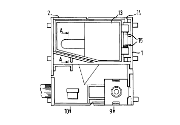
Referring to Figure 1, a coin valitator consists of a body 1 inrhl~ing a coin
inlet 2 into which coins are inserted from above so as to fall onto an inclined
CA 022~632 1998-11-19
WO 97/46984 PC'r/GB97/01358
coin rundown surface 3 and then roll edgewise through an inductive coin
sensing station 4 which includes sensing coils C1, C2, and C3 shown in dotted
outline. A coin 5 is shown on the inclined rundown surface 3, which moves
along a path 6 shown in dotted outline.
s
At the end of the inclined rundown surface 3, the coin falls through an
opening 7 towards the solenoid operated accept gate 8 that either allows the
coin to enter an accept path 9 or directs the coin along a reject path 10. The
accept gate is operated by circuitry responsive to the inductive sensing coils
10 C1- 3 at the sensing station 4 so that if the coin is determined to be of
acceptable characteristics, the gate 8 is opened by a sliding operation normal
to the plane of the paper in Figure 1, so that the coin can fall along path 9
and be accepted. The passage of the coin into the accept path may be directed
by a further sensor (not shown). Otherwise, the gate 8 remains closed so as
15 to block the accept path and as a result, the coin is ~flPcte~ by the gate into
the reject path 10.
The coin 5 runs in a gap between opposed side walls which, as can be seen in
Figure 2, 3 and 4, are c~fin~ by a wall 11 on the body 1 of the validator and
20 an interior wall 12 of a rundown gate 13 which is hinged about a sl1bst~nti~lly
vertical axis on a shaft 14 mounted on the body 1. The main rundown
surface 3 comprises a ledge formed on the bottom edge of the rundown gate
13 ~Figure 4). The rundown gate 13 is normally biasset to a closed position
by springs 15 so that the walls 11, 12 are generally parallel to one another as
2S shown in h~t~h~cl outline in Figure 3. However, the rundown gate 13 can be
hinged outwardly as shown in solid outline in Figure 3, by operation of a
reject lever in a manner known per se in order to release coins in the
~ rundown path, in the event of a coin jam. Also, the gate 13 can be opened
further in order to provide access to the rundown path as will be explained in
30 more detail hereinafter.
The three sensing coil circuits C1 - 3 at the coin sensing station 4 shown in
... . .
CA 022~632 1998-ll-l9
WO 97146984 PCT/GB97/01358
- 10-
Figure 1, are mounted in the validator body. Each circuit comprises a pair of
coils connected in series on opposite sides of the coin rundown path, one of
the coins being mounted behind the wall 11 and the other in the rundown
gate 13, and they are energised in order to provide an inductive coupling with
s the coin that runs along the coin rundown path 3. The coils are of different
geometrical configurations and are energised at different frequencies by a driveand interface circuit 16 shown in Figure 5 mounted in the validator body.
The different inductive couplings between the three coils and the coin have
been found to characterise the coin sllbsr~ntially uniquely, in terms of its
o m.ot~llic content and physical dim~nsions. The drive and interface circuit 16
produces three corresponding sensor signals xl, X2, X3 as a function of the
d;L~lent inductive couplings between the coin 5 and the coils C1 - 3. The
sensor signals xl, X2, x3 can be formed in a number of different known ways.
One way is described in detail in our GB-A-2 169 429. In this method, the
IS coils are infhl(~ec~ in individual resonant circuits which are mqinr~in~cl at their
natural resonant frequency as the coin passes the coil. The frequency ~hang~oc
on a transitory basis as a result of the momentary change in impedance of the
coil produced by the inductive coupling with the coin. This change in
impedance produces a change both in amplitude and frequency. As described
20 in our prior speçificltion, the peak amplitude deviation is monitored as the
coin passes the coils, and is riigiticerl in order to provide the sensor signal x for
each coil circuit. By mqint~ining the drive frequency for the coil circuit at its
natural resonant frequency during passage of the coin past the coil, the
arnplitude deviation is emphasised so as to aid in discrimin~tion be~w.~l1
2S coins. However, the signals can be formed in other ways, for example by
monitoring the frequency produced as the coin passes the coils and reference
is directed to GB-A-1 452 740, or by monitoring phase ~hange5 as a coin
passes the coils.
30 In order to determine coin anth~nticity, the three sensor signals xl, X2, X3
produced by the coin under test are fed tO a mi~uprocessor 17 which is
coupled to memory means in the form of an EEPROM 18 in the validator.
CA 022~632 1998-11-19
WO 97/46984 PCT/GB97/01358
- 11 -
The microprocessor 17 compares the sensor signals derived from the coin
under test with corresponding stored values held in the EEPROM 18. The
stored values are stored in terms of windows having upper and lower limits.
Thus, if the individual sensor signals xl, X2, X3 fall within the corresponding
s windows ~csori~te~ with a true coin of a particular denomination, the coin is
considered to be acceptable, but other~vise is rejected. If acceptable, a signal is
provided on line 19 to a drive circuit 20 which operates the gate 8 shown in
Figure 1 so as to allow the coin to pass to the accept path 9. Otherwise, the
gate is not opened and the coin passes to the reject path 10. During the coin
o validation process, the microprocessor compares the sensor signals xt, x2 and X3
with a number of different sets of operating window data appropriate for
coins of different denominations so that the coin validator can accept or rejectmore than one coin of a particular currency set.
~s The present invention is concerned with providing the stored data in the
memory 18 of the validator that can be used for comparison purposes with
the coin parameter signals derived from coins under test. Validators that are
mass produced to the same design do not have exactly the same characteristics
as a result of manufacturing tolerances. Consequently, the value of the data
20 stored in the EEPROM 18 needs to be slightly d;r~erell~ from validator to
validator in order to optimise coin discrimination between coins of different
denomin~ti~ns. The present invention is concerned with optimi~ing the
values of the stored data in order to compens~tP for individual differences in
the characteristics of the validators, which occur from validator to validator.
2S
Examples of the calibration process according to the invention will now be
described. In the following examples, calibration values of the individual
sensor signals xl, X2, X3 are derived from an individual validator during a
calibration procedure and the resulting calibration values of the sensor signals30 are then compared with sirnilar signals derived from an ensemble of coin
validators ~ a~ red to the same design as the validator being calibrated.
This enables the characteristics of the individual validator to be determined so
. , , . ... ~ ,,
CA 022~632 1998-11-19
WO 97/46984 PCT/GB97/01358
- 12 -
that coin parameter data represenr~tive of acceptable coins can be suitably
programmed into the validator, taking account of its individual characteristics.
The calibration process can be considered to consist of three major steps as
s shown in Figure 6. In the first step S1, an ensemble of data is collected
concerning the characteristics of an ensemble of coin validators all
manufactured to the same design. At step S2, an individual validator to be
calibrated, is characterised with reference to the ensemble data collected at step
S1. At step S3, the individual validator is ~e~irltec~ with coin parameter
o reference data represPnt~tive of acceptable coins of d;r~e.c~l~ cJPnomin~~ions~
the reference data having been sPIected in dependence upon the result of the
charaaerisation step S2. Three main d;frtrent characterisation and clP~ tion
methods will be described in detail hereinafter.
s In the following examples, the ensemble data collection step S1 and the
characterisation step S2 both make use of a calibration key K and an example
is shown in Figure 7.
The key consists of a metal plate, typically made of brass or some other
20 suitable alloy such as nickel copper, in order to produce a particular inductive
coupling with the coils C1, C2 and C3 at the sensing station 4 shown in
Figure 1. The calibration key K is inserted into the validator at a fixed, static
position as shown in Figure 8. The key K is inserted into the validator by
opening the rundown door 13 and placing the key on the coin rundown path.
2S The key K is configured so that it self-aligns at a particular location. It
includes a pin P which locates in a recess R in the rundown door 13. This
can be seen in Figure 8. The key has a peripheral configuration which
completely overlies the rli~mPt~r of coil C3 and partially obscures coil C1 and
C2. Thus, different inductive couplings are formed with the coils C1, C2 and
30 C3 individually. The key K thus provides a reference against which the
validator can be calibrated in terms of the inductive coupling of the sensor
coils C1- C3. The reference is d;~r.,e.l~ from the inductive couplings
,
CA 022~632 1998-11-19
WO 97/46984 PCT/GB97/01358
- 13 -
produced by coins under test. As will be ~pparent hereinafter, keys of
different materials and/or shapes may be used in the method according to the
invention to produce different sets of calibration values of the sensor signals.Also, instead of self-locating in the rundown path, the key may be inserted in
- s a key carrier (not shown), which itself is inserted into the path to locate the
key in place next to the coils C1-3.
The data collection step S1 for the ensemble of coin validators will now be
described with reference to Figure 9. At step S1.1 the first validator of the
~o ensemble is conn~cte~ to an external processor 22 (shown in Figure 5) such asa personal computer, by means of a connection 21 ~:igures 5 and 8) to the bus
of the microprocessor 17. Then at step S1.2, a first calibration key K, is
inserted in the coin rundown path in the manner shown in Figure 8. The
sensor coil circuits C1, C2 and C3 are sequentially energised, one at a time, by~s the driver circuit 16 shown in Figure 5 so as to produce sequential calibration
values of the sensor signals xl, X2, X3. It will be understood that these signals
are digital. Rec~llce the key is located in a static position, the coil circuits can
be energised for a longer period than for a coin rolling along the rundown
path, perrnitting highly accurate calibration values to be obtained. The
20 microprocessor 17 is configured to send the calibration values to the external
processor 22, where they are stored.
At step S1.3, the first key Kl is replaced by a second calibration key K2 which
may be made of a d;~.~.lt material and/or which is of a different shape, so as
2S to produce a second, d;ffe~ t set of inductive couplings with the coils C1,
C2, C3. The encl~;isalion process is repeated and the calibration values of the
coin signals for the second key are similarly stored in the external processor.
,.
Then the key K2 is removed and, at step S1.4, a set of known true coins of a
30 particular denomin~tion~ is fed into the validator. The values of the sensor
signals xl, X2, X3 produced by the known true coin are directed by the
microprocessor 17 to the external processor 22, where they are averaged for
, .~ . ... .
CA 022~632 1998-11-19
WO 97/46984 PCT/GB97/01358
- 14 -
each signal x" x2, x3, and the average values are stored.
At step S1.5, the process is repeated until sets of data have been collected from
all of the coin validators in the ensemble. The ensemble may typically
s comprise 50-200 validators.
When all of the data has been collected from the validators of the ensemble, it
is processed at step S1.6 in the external processor 22.
o In the first example of the invention, an average value of the data produced
for each of the coils is produced for the ensemble of validators. The data
received from the coils C1, C2 and C3 for the ensemble of validators is
considered separately. In this exarnple, the outputs from the coils C1 will be
considered and it will be understood that the outputs from coils C2 and C3
s are processed in a similar way. Firstly, an ensemble average value kl,V is
produced for the values of the sensor signal xl produced by the validators of
the Pncemhle in response to the first calibration key K1. A sirnilar signal k2,Vis produced from the calibration values of xl produced in response to the
second calibration key K2 for the ensemble. Additionally, an average
20 ensemble value t,v is produced for the stored value of the sensor signal xl
produced in response to the true coin introduced at step S1.4. Thus, the end
of step S1.6 (Figure 9) ensemble ~v~...ges kl~V, k2,V and t~v are produced in
respect of each of the coils C1, C2, and C3 respectively, which are stored in
the external processor 22. This data can then be used in a process vhich
2S allows individual validators to be characterised as they are manufactured, atstep S2 of Figure 6. This step will now be described in more detail with
reference to Figure 10.
Step 52.0, denotes the start of a procedure in which a newly m~m~f~ red30 validator from the production line is characterised in respect of its individual
characteristics that result from m~ntlf~lring tolerances during the pro~lction
process. At step S2.1 the validator is cor-necte(~ to the external processor 22
CA 022~632 1998-11-19
WO 97/46984 PCTIGB97/01358
- 15 -
in the manner shown in Figure 5 and a first key K1 is inserted into the coin
rundown path of the validator as shown in Figure 8. The key K1 is of the
same design as the key Kl that was used during the data collection process of
Figure 9 and hence has the same key characteristics. At step S2.2, the sensor
s signals xl, x2, x3 are measured to provide individual calibration values Ikl for
the validator. The calibration value Ikl for each coil circuit C1 - C3 is then
stored in the external processor 22.
At step S2.3, the process is repeated in respect of the second key K2 that was
o used during the data collection process of Figure 9, namely with a second key
K2 with the same characteristic as K~. The resultant coin calibration value Ik2
for each of the coils is stored in the external processor 22.
When both of the keys have been inserted and removed from the validator,
s the process moves to step S2.4 at which the individual values Ikl and Ik2 are
compared with the corresponding average values k1,V and k2~V. Referring to
Figure 11, it has been found according to the invention that a plot of the
calibration values Ikl, Ik2 against the corresponding average values k1~V and
k2~V ~proX;m~tes to a aL~digh~ line when considering one of the sensor coil
20 circuits e.g. sensor coil circuit C1. If additional different calibration keys are
used, the average values kn,v and the corresponding individual values Ikn lie
on the same straight line. Similarly, the value t~v and a corresponding
intividual value It for a true coin fall on the same straight line. Thus, by
referencing the value tlV tO the graph shown in Figure 11 (on the x axis) it is
2S possible to read off from the graph (on the y axis) an individual true value for
the particular coin denomination, for the individual validator being calibrated.
In this exarnple of the invention, data concerning the slope and intercept of
the graph shown in Figure 11 is stored in the individual validator. It will be~0 understood that the straight line graph shown in Figure 11 is of the form
y - mx + c
where m is the gradient and c is y axis intercept and so from the values Ikl
CA 022~632 1998-11-19
WO 97/46984 PCT/GB97/01358
- 16-
and Ik2 derived from the individual validator to be calibrated, together with
the average values k1,V and k2,V it is possible to compute the value of the
intercept c and the slope m of the graph. The values m and c are computed
by the external processor 22, using the data collected during steps S1 and step
s S2.2, at step S2.4 shown in Figure 10 and then, at step S2.5, the values of m
and c are stored in the memory 18 of the individual validator being calibrated.
Corresponding values of m and c for each of the sensor coil circuits C1, C2
and C3 are stored in the memor,v 18.
JO Thereafter, the individual validator is ~le~ t~ to accept true coins of a
number of different denominations (step S3 of Figure 6) which will now be
described in detail with reference to Figure 12.
At step S3.0, the external processor 22 is connected ~o an individual validator
s and at step S3.1, the slope and intercept parameters m and c are read from thememory 18 of the validator for each of the coil circuits C1, C2 and C3. At
step S3.2, the straight line graph of Figure 11 is effectively reconstructed by
the processor 22 and then the previously colllpuLed average value t,v for a truecoin is interpolated so as to derive an individual true value for the validator
20 concerned. This can be understood by referring to Figure 11. An individual
true value It for the validator can be determined from the y axis of the graph,
at the point of intersection of the x-ordinate value t~v and the line of the
graph. It will be understood that the processor 22 can readily compute this
value from the value t~v and the retrieved values of m and c, for each of the
2S sensor coil circuits C1, C2 and C3 respectively. The resl.lring individual
values It for the three coil circuits C1, C2 and C3 are then stored in the
memory 18 of the validator, at step S3.3. In fact, as previously mentioned,
the individual values are stored as windows with upper and lower limits
disposed above and below the value It, in order to provide an acceptance
30 window to take account of d;r~tnces in the coin signals produced by
d;rr~.c.l~ true coins of the same denomination, which in practice are found to
occur from coin to coin.
CA 022~632 1998-ll-l9
WO 97/46984 PCT/GB97/01358
- 17 -
The validator is then ready for operation and the stored windows can be
compared with the sensor signals x" x2, and X3 produced by coins under test
that pass through the validator.
s It will be understood that during the data collection step of S1, appropriate
mean values for a number of d;r~eltnt true coins can be produced by feeding a
set of coins of di[~r~ denorninations through each of the validators of the
ensemble and producing corresponding averages; step S1.4 can be repeated for
different true coins, so that during the de~ir3tion step S3, the routine S3.3 can
o be repeated for different true coins, to enable windows for true coins of
d;f~elen~ denominations to be stored in the memory of the validator, to allow
it to validate a number of different coin denominations.
It is not necessary to program acceptance windows for all of the true coins at
s the time of manufacture. It is possible to repeat the ~e~ir~tion step S3, later,
in the field if necessar,v, in order to change the coin denominations to be
accepted by the validator. To this end, the external processor 22 is conn~r~e~
to the validator, the stored values of m and c are extracted at step S3.1 and
then, at step S3.2, new individual values It are computed as previously
20 described, using values t,v appropriate for new acceptable coins for the
validator.
In a second exarnple of the calibration process, instead of forming the average
values klV and tlV~ a ~at~hl~e of validator data sets are derived from the
2S ensemble of coin validators in the data collection step S1. Each data set
consists of the calibration value produced in response to at least one of the
keys K, or K2 and a number of true coins Tn that are passed through each
validator of the ensemble. Thus, each data set comprises typically values kl,
k2 of the sensor signal together with values tl, t2, t3 and t4 produced in
30 response to corresponding true coins T1, T2, T3 and T4 passed through the
validator. Typically, 50-200 such data sets are produced from the validators of
the ensemble and a corresponding plot of the data is shown in Figure 13.
.... . . . . . . ....
CA 022~632 1998-11-19
WO 97/46984 PCTIGB97/01358
- 18 -
During the characterisation step S2, data concerning the calibration values of
the sensor signal for the two keys K1 and K2, namely Ikl and Ik2 are stored
in the memory 18 of the individual validator. This process is shown in Figure
14 in which steps S2.1 to step S2.3 are performed as previously described and
s then the reslllting values Ikl and Ik2 are stored in the memory 18 of the
validator being calibrated.
The ~e~lic~tion process is shown in Figure 15. With the external processor 22
connected to the validator, the key parameters Ikl, Ik2 are extracted from the
o memory 18 of the validator at step S35, and then at step S3.6, these values are
compared with the stored data sets that were collected during step S1. Ihe
two values Ikl and Ik2 are colllpdred with the values of the data sets from the
ensemble thereof in order to choose the set which most closely resembles the
key values stored in the validator. In this way, a data set is chosen which
s most closely appro~im~teC to the characteristics of the validator being
de~ te~ In a modification, a number of the data sets from the ensemble
may be chosen and the values thereof a~.agod, to reduce errors in the data.
Then, appropriate true coin values e.g tl, t2, t3 can be programmed into the
20 memory 18 of the individual validator, depending on which coins it is desiredto validate. As previously described, windows may be associated with each
stored value in order to accommodate the dirrclences in signals that occur for
dirr~r~ true coins of the same denomination.
2S In a third exarnple of a method according to the invention, the information
held in the database shown in Figure 13 is rearranged to allow selective
r~log~ ming of validators in the field, for exarnple by tr~ncmitting
appropriate reprogr~mming data over a telephone line from the central station
to the validator. It is ~Csllm~o~ that the validator has in its memory a key
30 parameter Ikl and that its microprocessor includes a reprogra~ming sub-
routine which can operate at the validator itself, rather than using an externalprocessor such as processor 22.
,
CA 022~632 1998-ll-l9
WO 97/46984 PCT/GB97/01358
- 19 -
The information concerning the r~ltlhace of Figure 13 is held at a central
location for trancmi~sion to validators in the field. The database is organised
in such a way that the information can be readily tr~ncmitte~ to the validator.
In this example, it is assumed that the validator has already been pro~la~ lcd
s with appropr;ate true coin values for coins tl, t2 and t3 in the manner
described previously with reference to Figure 15, and that subsequently, it is
desired to prograrn a value t4 for an additional true coin. To achieve this,
the (~t~h~ce of Figure 13 is reorganised such that the values of t4 for each data
set are considered as a difference relative to the value kl for the set. Thus, for
o each data set, the value of t4 can be written as follows:
t4 = kl + ~
It will be understood that the individual values of t4, kl and ~ can be
d;rl~le.l~ in each data set. The data of Figure 13 is reorganised so as to
provide a series of "data bins" into which values of kl between individual
s ranges are collected. This is shown as step S4.1 in Figure 16. It will be
understood that the values of various parameters can be considered as count
values as a result of the digital nature of the signals. In the following Table,three data bins are shown by way of example, for count values of k between
100.00 - 100.99; 101.00 - 101.99 and 102.00 - 102.99 although in practice,
20 many more are used.
Table
parameter bin 1 bin 2 bin 3
kl 100.00- 100.99 101.00-101.99 102.00- 102.99
2S ~SIV 10.25 10.27 10.24
The various values of the data sets are collected into the bins for different
values of k and at step S4.2, the values of ~ corresponding to the data sets foreach bin are averaged so as to form a value ~,~. The resulting values of the
30 data bins and corresponding values of ~lv are then stored in a memory at the
central location.
CA 022~632 1998-11-19
WO 97/46984 PCT/GB97101358
- 20 -
When it is desired to program the value of t4 into the memory of a validator
at a remote location, the bin data as shown in the Table is tr~ncmittecl
digitally over a telephone line to the validator. For example, the validator
can be considered to be at a remote location relative to the processor 22 of
s Figure 5, e.g. in a pay telephone. The processor 22 stores the bin data shown
in the foregoing Table, and is connPcte~ via a telephone line to the bus of the
microprocessor 17 through interface circuitry (not shown). After an initial
han~lch~k~ procedure, the validator switches to a calibration mode and data
concerning the ranges of values of kl for the suc~essive data bins, together
o with the associated values of /~,v are tr~ncmitted to the validator from the
processor 22, as shown at step S4.3. The validator retrieves its stored value ofIkl and at step S4.5, notes when a bin which contains the value is received
from the central location. The corresponding value of ~,,v for the selected
bin is added at step S4.5 to the stored value of Ikl so as to produce an
s appropriate value of t4 for the validator. Appropriate window values are
computed around the value of t4 and the resulting upper and lower window
lirnits are stored in the memory 18 of the validator. It will be understood
that in practice bin data for more than one calibration key will be used.
20 It will be appreciated that this procedure permits selective l~rog~...,..ing of
the memory 18 in the field either to change the values associated with
particular coins or to provide data for a new coin denomin~tion. It will be
understood that the data of the Table may be broadcast to a plurality of
validators in the field cimlllt~neously~ in order that they may be
2S reprogrammed cimlllt~neously, without the need to extract their individual
calibration values for external processing. Alternatively, the data of the
Table may be tr~ncmitted to each validator individually in response to a
request rece;~ed from the validator. For example, for a coin validator in a
telephone coin box, when a new validator is fitted, it may be plug~ ed by
30 the downloading the Table data through the telephone system to the coin
box, from a remote location, the downloading being initi:~te(~ by a request
from the coin box control circuitry, in response to detection that a new
.~ .,
CA 022~632 1998-ll-lg
WO 97/46984 PCT/GB97/013S8
- 21 -
validator has been fitted, e.g. in the event of a repair.
It has been found that the use of static calibration keys K has the advantage
that the count values of the sensor signal that are produced have an improved
5 accuracy as compared with the prior art arrangements which use tokens or
coins which pass on a transitory basis past the coils Cl, C2, C3. Also, it has
been found that the use of data from an ensemble of coin validators gives a
very accurate correlation between the individual value stored in the memory
of a validator, for an acceptable coin, and the actual value needed to achieve
o acceptable coin discrimination. The use of the ensemble data has the
advantage that it is no longer necessary to pass large numbers of coins of
different denominations through each validator during manufacture, to
calibrate its memory. Furthermore, the method may provide data stored in
the memory of each validator which permits accurate reprogramming if it is
s desired to use the validator with a different currency set.
In practice there may be more than one production line for validators of the
same design, so that it would be desirable to have more than one set of keys
for calibration purposes. However, the keys need to have demonstrably
20 i-~entical characteristics, from set to set, in order to produce consistent
calibration. In order to meet this requirement, the characteristics of the keys
can be compared relative to a master key, in terms of the values x1, x2 and x3
that they produce in an individual validator, and the difference between the
value of say x~, for one of the keys and a corresponding master key, can be
25 stored in association with the key, and used as an offset in the actual
calibration process.
Whilst the use of static keys is advantageous, it is possible to perform the
method according to the invention by replacing the static key with known
30 true coins which function as mobile calibration keys that are fed through the validator in the same manner s the coin being vali~lte~l For the second
example described with reference to Figure 13 to 1~, the values of known true
CA 02255632 1998-11-19
WO 97/46984 PCT/GB97/01358
coins T1 and T2 could be used for characterising the validator at step S2
(Figure 14) and the values thereof could be compared with the values in the
~qtqhqce during the .le~ tion step S3 ~igure 15).
5 The term "coin" herein includes a token or similar coin-like item of value.