Note: Descriptions are shown in the official language in which they were submitted.
ui <=,., ' ~r=} tS:f ..::s:f I=~lfi~: +i ~
lrCA 0225'5642 1998-11-19 -
1
COIN TESTl~*1Cr A_PPARATI:)S Ax,,'T) kfE7Hr'1n
The present invention rctates to coin testing apparatus, and a method of
recogrnising coins.
Coin testing systems, or coin valuators, are used to recognise and evaluate
different coins, for exaMple, in vendine machines and telephones. There are
various
e1cctromechanicat and electromagr,etic coin valuators available which are in
use fcr
various purposes; e.g. vending machines, public and private telephones, etc.
Such
valuators may be used in many types of vending machine, or slot machine, in,
for
~ ..
example, airports, railway stations, garnblFngmachines, industries, schools,
hospitals,
hotels, or offshore platforms.
Such coin valuators in operation in vending machines and telephones are
generally very limited as regards t.'~e numbcr of different types of coin that
can be
evalu4tPd.
British Published Patent Application GB-A-2,212,313 discloses a coin sorning
apparatus in which a beam of light is directed at an anole towards the edgeof
a coin.
If the coin is of the right diameter, then part of the beam of light passes in
a straight
line through to a first detrctor and part of the beam of light is reflected
(scattcred) to
a second detector that is not on the straight through path. The system of GB-A-
..212.313 relies upon some light being received by both= detectors to identify
that the
coin is ef just the right diameter to partially reflect the light beam. If no
light is
;0 received by eithcr detector, or all of the light is received by the
straight through
detector, then the coin is not of the desired diameter. The system suggests a
laser
diode as one possible light source.
F..uropPln Published Patent Application EP-A-0,629,979 discloses a system
ensuring that a supply of new coins have the correct size by using a light
current and
a linear sensor array.
~~~~0
_ ., .,.. _... , .., , .,
_ .
~;~ . ~. =~~:;. .a'~~ CA 02255642 1998.-11-19
IA
Summarv of the Invetion
Accord'zng to a first aspect of the present invention, there is provided a
method
of :.cin testing, in which a laser beam is directed onto a face of a coin and
a laser
detector is used to obtain an indication of a dimensional cha:acteristic of
the face of
the coin, charactcrised in t.'lat said laser detector detects where thc laser
beam is
intercepted by the coin and where the laser beam is not intercepted by the
coin.
The length may be deterrrtined or decected of at least part of at teast one
elo:tgate strip of the face of the coin.
~. , ... _. = -_~'. ~
S~S
CA 02255642 1998-11-19
WO 97/44760 PCT/IB97/00569
2
The lengths may be determined or detected of at least parts of a plurality of
elongate strips of the face of the coin.
The beam may scan the strips, or the parts thereof, one after another.
The beam may have a fan-like shape so as to impinge upon the whole of the or
each said strip, or part thereof, simultaneously.
The laser detector may comprise many side-by-side pixels, each individually
capable of detecting laser radiation.
Preferably, the beam is stationary and the coin moves past the beam.
The coin may rotate as it moves past the beam.
The coin may move along a guide as it moves past the beam.
The coin may be in free fall as it passes the beam.
One end of the or each said strip may be at an edge of the coin and another
end
of the strip may be at a predetermined location which is not at an edge of the
coin.
A second laser beam may be directed at an edge of the coin and may be detected
so as to determine a characteristic of the edge and/or thickness of the coin.
A dimensional characteristics of a groove and/or a ridge on the edge of the
coin
may be determined or detected.
The number of grooves and/or ridges in a predetermined distance on the edge of
the coin may be counted.
-.-<CA 02255642 1998-11-19'~ .r
3
The second laser beam may be de:ivcd from the first-mentioned laser beam.
The second laser bea,Yn may be dcrived from the first-mentioned laser bean, by
rr.eans of a prism which redirects a portion of the first-mentioned laser
beam.
Preferably, at the point of interception of thc coin and the laser, the coin
is
absolutcly perpendicular to thhe laser beam.
At the point of interception of the coin and the laser, the laser bear,t mav
be
substantially in the forrri of a thin plane of laser radiation.
Accr-rding to a sccond aspect of Ihe present inveatiun, there is provided
apparatus for coin testing, comprising
~S :' =
a laser source adap[ed and arranged to direct a lase: beam onto a face of a
coin.
a laser detector, and
a signal-processor adapted and arranged to obtain from an output of the laser
detector an indication of a dimensional eha.,-aeteristic of the face of the
ciin;
cr.araete:ised in that
said :aser detector adapted and ar*anged to dztect where the iaser is
intercepted
by the coin and where the ;aser is not intercepted by the coin. ~
Preferably, the apparatus is adapted to determine or detect the length of at
least
part of at least one elongate strip of the face of the coin.
The app.a.ratt:s may bc adapted to determine or detect :he lengths of at
lear,t parrs
of a plurality of elongate strips of the face of the coin.
?p
The beam may be adapted to scan said strips, or said parts tnereof, one after
another.
The beam may have a fan-like shape so as to il rnpinge upon the whole of the
or
each said strip, or part thereof, simultaneously.
CA 02255642 1998-11-19
WO 97/44760 PCT/1B97/00569
4
Preferably, the laser source and hence the beam are stationary and the
apparatus
is adapted to cause the coin to move past the beam. -
The apparatus may comprise a guide for the coin to move along as it moves past
the beam.
The apparatus may be adapted so that, in use, the coin is in free fall as it
passes
the beam.
In use, one end of the or each said strip may be at an edge of the coin and
another end of the strip may be at a predetermined location which is not at an
edge of
the coin.
The apparatus may comprise means to direct a second laser beam at an edge of
the coin, means to detect where the second beam is intercepted by the coin,
and means
to determine therefrom a characteristic of the edge and/or thickness of the
coin.
The apparatus may comprise means to derive the second laser beam from the
first-mentioned laser beam.
The means to derive the second laser beam from the first-mentioned laser beam
may comprise a prism which redirects a portion of the first-mentioned laser
beam.
The laser detector may comprise many side-by-side pixels, each individually
capable of detecting laser radiation.
According to a third aspect of the invention, there is provided a coin testing
apparatus comprising:
a laser source adapted and arranged to direct a laser beam onto a coin;
CA 02255642 1998-11-19
WO 97/44760 PCT/IB97/00569
5 a laser detector adapted and arranged to detect where the laser is
intercepted by
the coin and where the laser is not intercepted by the coin;
a coin guide arranged to enable the coin to travel along a specified path
along
which path the coin is able to intercept a portion of a laser beam passing
between the
laser source and the laser detector; and
a signal-processor adapted and arranged to obtain an output of the laser
detector;
wherein the proportion of the laser beam that is intercepted provides at least
one
measure of a geometric dimension of the coin, the coin being recognisable by
comparing said measure of the coin with corresponding measures of a number of
known
coins.
At least one measure may be made of a geometric dimension on the face of said
coin and another measure may be made of the thickness of said coin in order to
compare
said measures of the face and thickness with corresponding measures of said
number of
known coins.
A range of geometric dimensions may be measured iteratively to provide an
integrated area measurement of a surface region of said coin, said coin may be
recognisable by comparing said area measurement of said coin with
corresponding area
measurements of said number of known coins.
A dimensional characteristic of a groove and/or a ridge on the edge of the
coin
may be determined or detected.
The number of grooves and/or ridges in a predetermined distance on the edge of
the coin may be counted.
The measure of a geometric dimension of said coin, and said corresponding
measures of said number of known coins, may all relate to measurements of
coins which
are smaller than the diameter or, in the case of irregular-shaped coins, the
maximum
cross-section of each respective coin.
CA 02255642 1998-11-19
WO 97/44760 PCT/IB97/00569
6
The laser beam passing between said laser source and said laser detector may
travel therebetween via a circuitous non-direct route.
The laser beam may be directed along said circuitous non-direct route by one
or
more of mirrors or prisms.
The path may comprise a passageway, having a lower boundary, along which
said coin is able to travel through the apparatus whilst supported
continuously at its
peripheral edge by said lower boundary of said passageway.
The laser source may be mounted so as to direct a laser beam from one side to
the other of a portion of said passageway, substantially perpendicularly to
the main
plane of said coin in said passageway, so as to be intercepted by upper
regions of said
coin as it travels through said portion of said passageway.
The laser detector may comprise a linear array of many side-by-side pixels,
each
individually capable of detecting laser radiation.
The array may extends substantially parallel to said main plane, and
transversely
with respect to the direction of travel said coin along said portion of the
passageway,
and may have a lower end spaced at a first distance from said lower boundary,
which
first distance is less than the minimum diameter of said number of coins, and
an upper
end spaced at a second distance from said lower boundary, which second
distance is
greater than the maximum diameter of said number of coins, said laser detector
may be
operable to produce an output dependent upon the number of said pixels from
which
said laser beam is blocked, at a plurality of successive sampling instants, by
a coin
travelling along said portion of the passageway, so that said output can be
compared
with predetermined reference data records to ascertain which of those records
corresponds to said output.
CA 02255642 1998-11-19
WO 97/44760 PCT/IB97/00569
7
The coin may travel along said path such that at the point of interception
said
coin is absolutely perpendicular to said laser beam.
Preferably, the laser beam that is intercepted by said coin is, at the point
of
interception, substantially in the form of a thin plane of laser radiation.
According to a fourth aspect of the invention, there is provided coin testing
apparatus comprising:
a coin guide defining a coin passageway, having a lower boundary, along which
a coin can travel through the apparatus whilst supported continuously at its
peripheral
edge by said lower boundary;
a laser source being mounted for directing a laser beam from one side to the
other of a portion of said passageway, substantially perpendicularly to the
main plane of
a coin in the passageway, so as to be intercepted by upper regions of said
coin as it
travels through said portion of said passageway; and
laser detector comprising, at said other side of said portion of the
passageway, a
linear array of laser receiving locations, which array extends substantially
parallel to
said main plane, and transversely with respect to the direction of travel of
the coin along
said portion of the passageway, and has a lower end spaced at a first distance
from said
lower boundary, which first distance is less than the minimum diameter of a
number of
coins with which the apparatus is to be used, and an upper end spaced at a
second
distance from said lower boundary, which second distance is greater than the
maximum
diameter of said number of coins, said laser detecting means being operable to
produce
an output dependent upon the number of said laser- receiving locations from
which said
laser beam is blocked, at a plurality of successive sampling instants, by a
coin travelling
along said portion of the passageway, so that said output can be compared with
predetermined reference data records to ascertain which of those records
corresponds to
said output.
CA 02255642 1998-11-19
WO 97/44760 PCT/IB97/00569
8
The apparatus may comprise more than one laser source and more than one laser
detector.
According to a fifth aspect of the invention, there is provided a method of
recognising a coin comprising the steps of:
i) making a coin travel along a specified path such that said coin intercepts
a portion of laser beam passing between a laser radiation source and a laser
detector;
ii) measuring the proportion of said laser beam that is intercepted as a
means of ascertaining at least one measure of a geometric dimension of said
coin,
iii) comparing said measure of said coin with the corresponding measure of a
number of known coins in order to recognise said coin.
The at least one measure may be made of a geometric dimension on the face of
said coin; and the method may further comprise the step of ascertaining the
measure of
the thickness of said coin in order to compare said measures with
corresponding
measures of said number of known coins.
The method may further comprise the step of ascertaining the measure of a
number of geometric dimension of said coin to provide an integrated area
measurement
of a surface region of said coin, said coin being recognisable by comparing
said area
measurement of said coin with the corresponding area measurements of said
number of
known coins.
The method may comprise the step of determining or detecting a dimensional
characteristic of a groove and/or a ridge on the edge of the coin.
The method may further comprise the step of counting the number of grooves
and/or ridges in a predetermined distance on said coin.
CA 02255642 1998-11-19
WO 97/44760 PCT/IB97/00569
9
In this description and the appended claims, the terms "laser source" and
"laser
detector" should be taken to cover any device or combination of devices which
fulfil the
fun.ction of providing a source of laser radiation, and detecting the laser
radiation,
respectively. The laser source and laser detector may each be a single
component, a part
of a component, or an assembly of parts, provided that each fulfils the
function of
enabling the working of the invention as claimed.
Further preferred features of the invention will be apparent from the claims
annexed hereto and the subject matter of these claims are hereby imported into
this
specification.
Drawines
In order that the invention might be more fully understood, embodiments of the
invention will be described, by way of example only, with reference to the
accompanying drawings, in which:
Figure 1 shows a cross-sectional side view of a first embodiment of a coin
testing apparatus;
Figure 1 A shows components of the first embodiment in their relative
orientation to one another;
Figure 1 B shows a cross-sectional side view of a housing used in the
embodiment of Figure 1 without the internal components, for the sake of
illustration;
Figure 1 C shows an external side view of the housing of Figure 1 B;
Figure 1 D shows a perspective view of the housing of Figure 1 B
CA 02255642 1998-11-19
WO 97/44760 PCT/IB97/00569
5 Figure 2 shows a cross-sectional side view of a second embodiment of a coin
testing apparatus;
Figure 2A shows components of the coin testing apparatus of the second
embodiment of Figure 2 in their relative orientation to one another;
Figure 2B is a perspective three-dimensional view of components of the second
embodiment illustrated in Figure 2 and 2A;
Figure 2C shows another view of the second embodiment of Figure 2, 2A and
2B, illustrated with a coin shown as rolling from right to left across the
diagram;
Figure 2D illustrates the coin guide of Figure 2A installed in a tilted
orientation;
Figure 2E shows an arrangement for measuring coin thickness;
Figure 3 is an illustration which uses the letters X, Y and Z to indicate the
spatial
arrangements of three linear arrays used in a further embodiment;
Figure 4 is an illustration of a third embodiment in which the coin intercepts
the
laser beam as the coin is in free fall. An arrow is used to indicate the
direction of the
fall of the coin;
Figures 5 and 6 are schematic diagrams of alternative embodiments which serve
to illustrate that the invention may also be able to incorporate laser sources
and laser
detectors that are not positioned perpendicularly to the main plane of the
coin;
Figure 7 shows a laser unit used in the first embodiment of Figure 1;
Figure 7A shows the use of a Powell lens to focus the laser beam;
CA 02255642 1998-11-19
WO 97/44760 PCT/IB97/00569
11
Figure 7B shows to top view of the laser beam of Figure 7A, illustrating that
the
laser beam formed by the Powell lens is in the form of a plane or line of
laser radiation;
Figure 8 shows several views of a sensor unit used in the embodiments of
Figures 1 and 2;
Figure 9 shows an electrical block diagram of intemal parts of the sensor unit
shown in Figure 8;
Figure 9A is a timing diagram of a linear array, in parallel connection,
showing
pulses relating to the sensor unit of Figure 8 and 9;
Figure 10 is a circuit diagram used in the first generation electronics used
in the
embodiment of Figure 1;
Figure l0A shows a block circuit diagram of a clock signal generating circuit
used in the embodiments of Figures 1 and 2;
Figure l OB shows a "power-on" circuit;
Figure 11 is a circuit diagram of the laser power supply;
Figures 11A show Y-Z Sensor Array pin-out used in the apparatus of Figures 1
and 2;
Figure 11B is a diagram which explains the pixel layout;
Figure 11 C shows three level converters for analogue to digital conversion;
Figure 12 shows a block circuit diagram of a counter circuit used in the
embodiments of Figures 1 and 2;
CA 02255642 1998-11-19
WO 97/44760 PCT/IB97/00569
12
Figure 12A shows two circuits of latches;
Figures 12B show a block circuit diagram of two buffer interfaces;
Figures 12C shows a block circuit diagram of a main control circuit used in
the
embodiments of Figures 1 and 2;
Figure 12D shows two static memory RAM circuits;
Figure 12E shows a flash memory EEPROM circuit;
Figure 12F shows a LCD driver, relays and photo-transistor driver;
Figure 12G shows a relay PIN driver and PIN photosensors;
Figures 12H and 121 show printed circuit boards useable in the circuitry of
the
embodiments;
Figure 13 is a graph, shown on an xy axis, plotting the function for an
algorithm
which is used for calculations that are performed in an embodiment of the
invention;
Figure 13A illustrates an embodiment where the coin is identified with
reference
to characteristics of grooves in the edge of the coin;
Figure 14 is a block diagram illustrating components embodiments of the
invention with respect to the electrical components.
The drawings are provided for the purpose of illustration only and therefore
are
not necessarily drawn to scale.
CA 02255642 1998-11-19
WO 97/44760 PCT/IB97/00569
13
In the embodiments, similar components are numbered with the same numbers
for the sake of illustration. For example, the laser radiation sources in each
embodiment
would be labelled with the same reference numeral, but this should not be
taken to
imply that the embodiments are identical.
Description of Embodiments
First Embodiment
Referring to Figure 1, there is illustrated a first embodiment of the
invention, in
the form of a coin testing apparatus 20. The apparatus 20 comprises a housing
5.
A laser source in the form of a cylindrical laser unit 1 is slideably mounted
in a
cylindrical cavity 51 in the housing 5.
The laser unit 1 comprises a conventional laser diode 11 and lens groups (both
groups indicated by the numeral 12.) The laser diode 11 produces a laser beam
13
(shown with dotted lines in Figure 1). The lens groups 12 are designed to
convert the
laser beam 13 into a form such that the beam is in a fan-like shape when it
leaves the
front of the laser unit 1. The laser beam emanates from the laser diode 11 as
a point
source, and is spread into a fan-like shape by the lens groups 12 so that the
beam can be
used to impinge upon larger portions of the coin simultaneously.
The shape of the laser beam 13 is one that spreads in the form of a fan-like
laser
beam. In order to create this flat spreading laser beam, two sets of lenses of
differing
characteristics are used. A first group of lenses 12 act to highly collimate
the laser beam
having a rectangular cross-section. Another group of cylindrical lenses 12
cause the
cross-section of the laser beam to be elongated, such that the cross-section
becomes an
elongated rectangle, almost to the point of being a line. The laser beam 13
from the
laser diode 11 passes through these lenses. In Figure 1, the fan-like laser
beam is
CA 02255642 1998-11-19
WO 97/44760 PCT/IB97/00569
14
focused using lenses 12 in the laser unit 1, and by slideably adjusting the
position of the
laser unit I in the cavity 51.
The coin testing apparatus 20 further comprises a coin guide which includes a
channel 61 having a lower boundary 62 and an upper passageway 52, in which
there is
shown a coin 4. The coin is introduced to the passageway 52 by way of a coin
insertion
aperture 63 (best seen in Figure 1D.) The channel 61 guides the coin 4 along
the
passageway. The coin passageway 52 extends transversely through the housing
member
5. The coin 4 is supported continuously at its peripheral edge by the lower
boundary 62
of the coin guide. The coin 4 travels through the apparatus in a direction
perpendicular
to the plane of Figure 1.
On the far side of the channel 61 from the laser source 11, the housing 5
contains
a laser detector in the form of a sensor array unit 3. The array unit 3
comprises many
side-by-side individual high speed charge accumulators and pixels (not
separately
shown). These charge accumulators include pixels which are sensitive to laser
radiation
and are capable of detecting and measuring laser radiation energy levels. The
pixels are
arranged in a linear array, in a linear or grid-like orientation to form a
contiguous array
of pixels. Each charge accumulator, in its uncharged state, is able to become
charged
when the beam of a laser beam 13 shines on the particular pixel. The pixels
are
sufficiently sensitive to detect photons, which are an elementary component of
the laser
beam. The sensor array unit 3 also comprises pins 19 which are adapted to
connect the
sensor array unit 3 to an electronic circuit, described hereinafter.
The laser beam 13, generated by the laser diode 11, is directed towards the
sensor array unit 3. In the embodiment of Figure 1, after the laser beam
leaves the laser
diode 11, the laser beam 13 is directed to form a fan-like flat beam shape.
The reference
to fan-like refers to the spreading of the laser beam as it leaves the laser
diode. The
reference to the flat beam refers to the formation of a thin line, or linear
plane of laser
beam radiation. The plane of this fan-like beam of radiation is generally
directed
towards the centre of the linear array.
CA 02255642 1998-11-19
WO 97/44760 PCT/11397/00569
5
The laser beam 13 travels between the laser diode 11 and the linear array of
sensors 3. The laser beam 13 is directed axially along the cavity 51 and
across the
passageway 52. The axis of this laser beam 13 is substantially perpendicular
to the main
plane of the coin in the passageway. The laser beam 13 is directed onto a face
of the
10 coin 4 to be tested. The coin 4 intercepts a portion of this laser beam 13
that passes
between the laser diode 11 and the sensor array unit 3. In the present
embodiment, the
beam is stationary and the coin moves past the laser beam. A circular coin
rotates as it
moves past the beam, while a non-circular or polygonal-shaped coin would slide
past
the beam.
The sensor array 3 is able to detect where the laser is intercepted by the
coin and
where the laser is not intercepted by the coin, since those pixels which are
irradiated by
the laser beam will cause the charge accumulators to become charged, while
those
pixels that are shielded by the coin will not cause the charge accumulators to
be
charged. The information of the charged and uncharged accumulators is used to
obtain
an indication of a characteristic of the face of the coin, as will be
described below.
Referring to Figure 9, the pixels and charge accumulators work on the basis of
saturation by measuring the minimum and maximum absorbable quantum energy of
the
laser beam. When a pixel is excited to the level of around half of its maximum
saturation charge, the control logic of the pixel is able to determine the
accurate amount
of energy received by the pixel from the laser beam. The control logic then
determines
whether to consider the charge accumulator as being "0" for an uncharged
state, or "1"
for a charged state.
In the present embodiment, the plane of the linear sensor array unit 3 extends
substantially parallel to the main plane of the coin 4 in the passageway 52,
and
transversely with respect to the direction of travel of the coin along that
passageway. In
Figure 1, the lower end of the array 3 is spaced at a first distance d from
the lower
boundary 62, which first distance d is less than the minimum diameter of any
coin with
CA 02255642 1998-11-19
WO 97/44760 PCT/IB97/00569
16
which the apparatus is to be used. The upper end of the array 3 is spaced at a
second
distance D from the lower boundary 62, which second distance D is greater than
the
maximum diameter of any coins. The laser beam 13 will therefore be intercepted
by
upper regions of the coin 4 as it travels along the passageway.
It is preferable to allow upper regions of the coin 4 to be intercepted by the
laser
beam 13 to allow measurements to be taken of upper regions of the coin.
Alternatively,
measurements may be taken at other regions of the coin 4, such as side
portions.
However, when the coin is in contact with the lower boundary 62 of the coin
guide, such
contact would make it difficult to obtain accurate measurements for those
parts of the
coin which are in contact with the lower boundary 62.
Measurements of the coin need not be taken for the entire diameter or, in the
case of irregular coins, the maximum cross-section. By avoiding readings of
the
diameter or maximum cross-section, the problems associated with measuring the
portion
where the coin contacts the rolling surface are minimised.
The sensor unit of the linear array 3 produces electrical outputs, at
respective
successive sampling instants, which are dependent upon the number of the
pixels which
are blocked by the coin and the number of pixels which are not blocked. This
signal is
preferably sampled many times as the coin moves past the linear array 3, as
will be
described in more detail below.
The sensor unit of the linear array 3 is connected to a signal processor which
process these outputs to identify the coin concerned. The signal processor is
in the form
of microcontroller 14, which is illustrated in Figure 12C and 14. The
microcontroller 14
includes comparison means for determining which, if any, of a plurality of
predetermined reference data records correspond to the processed outputs. For
example,
the processed outputs from the linear array 3 are compared with data records
of a large
number of known coins. The coin 4 is identified by matching the processed
output
obtained from the linear sensor with the corresponding data record of the
known coin.
CA 02255642 1998-11-19
WO 97/44760 PCT/IB97/00569
17
The housing member 5 is made of a material which gives good absorption of
scattered laser radiation, for example a black polycarbonate material. The
external
aspect of the housing 5 is illustrated in Figures 1 C and 1 D. Other designs
may be
selected depending on the particular environments in which they are installed.
Moreover, in other embodiments of the invention, rather than the coin testing
apparatus
being installed in its own housing, it is possible for various components of
the coin
testing apparatus to be manufactured integrally as part of the device in which
it is being
used, for example, a vending machine or telephone. In these embodiments, the
coin
guide are provided as part of the components of the particular device. It is
conceivable
that the coin guide may not be a separately identifiable component. In such
embodiments, any feature of the overall device that serves to guide the coin
to be
intercepted by the laser beam may be regarded as fulfilling the function of
the coin
guide.
In other embodiments, the various structural components of the coin testing
apparatus may be moulded in one piece. For instance, mirrors and prisms may be
moulded from the same material as the housing and coin guide. One advantage of
moulding as a means of manufacture would be used to reduce the cost of
apparatus.
Figure 7 shows an alternative embodiment for constructing the lens groups. The
desired shape of the laser beam 13 is produced by using a collimating lens 75
and a line
generating lens 72 through which the laser beam from the laser diode passes.
The
fan-like beam is focused using the second series of lenses 12 in the laser
unit 1, and by
adjusting the axial position of the laser unit 1 in the cavity 51. By rotating
a front cell
assembly 73, the beam is focused and collimated, as illustrated in Figure 7. A
locking
ring 74 is used to secure the final position. The lens assembly may be rotated
using a
key supplied with the laser diode module in order to produce the best line of
incidence
of the laser beam 13 on the linear array 3. The greater the operating
distance, the longer
and thicker the line.
CA 02255642 1998-11-19
WO 97/44760 PCT/IB97/00569
18
Second Embodiment
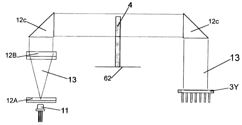
A second embodiment of the invention is illustrated in Figures 2, 2A and 2B.
This second embodiment is similar to the first embodiment, except that the
laser
detector comprises two linear arrays 3Y, 3Z. (For the sake of illustration of
the concepts
herein, X and Y refer to the orthogonal x and y axes terminology used in
engineering.)
A laser beam 13 emanates from the laser diode 11 and is refracted by lens 12a,
and further refracted by lens 12b.
The focusing of the laser beam into a line is achieved using a "Powell lens".
Lines of laser radiation focused by Powell lenses have the unique
characteristic of
having uniform intensity along the entire length of the line. The spreading
effect of the
laser beam is illustrated in Figure 7. Figure 7A shows the use of a Powell
lens 12 for
widening the angle of the laser beam 13. Figure 7B is a top view of the laser
beam
shown in Figure 7A which illustrates that the laser beam, formed by the Powell
lens, is
in the form of a thin plane of laser radiation.
By the time the laser beam reaches the point of interception with coin 4, the
laser
beam 13 is directed along a path substantially perpendicular to the main plane
of the
coin 4. A portion of the laser beam is directed at an edge of the coin 4 and
is intercepted
by the circumferential rim or edge of the coin 4. Part of the remainder of the
laser beam
strikes linear array 3Y. Thus, the linear array 3Y is able to determine a
characteristic of
the edge and/or thickness of the coin 4. Figure 2C illustrates a side view of
the coin 4
rolling past the linear arrays 3Y, 3Z.
At the same time, a portion of laser beam 13 is re-directed by a prism 12c.
Mirrors may be used instead of prisms. The prism 12c re-directs the beam
perpendicularly such that the beam is directed to strike the edge of the coin.
Only a
CA 02255642 1998-11-19
WO 97/44760 PCT/IB97/00569
19
portion of downwardly directed beam strikes the other linear array 3Z. Thus,
two linear
arrays are used to measure different portions of the surface and edge of the
coin 4.
An advantage of the beam being absolutely or at least substantially
perpendicular to the main plane of the coin 4, at the critical point of
interception of the
coin with the beam, is that the beam subsequently shines directly onto the
linear sensor
without any further deviation. Hence, the measurement taken at the linear
sensor would
be an accurate measure of the actual coin.
In contrast, in Figure 4, if the laser beam intercepts the coin at an acute
angle, the
measurement taken at the linear sensor will be slightly larger than the actual
size
dimension of the coin. However, the coin testing apparatus would still work
effectively,
provided the data measurements of known coins are calculated taking this
factor into
account. Hence, it is preferable, but not essential to the invention in its
broadest aspect,
that the beam be absolutely perpendicular with the plane of the coin at the
critical point
of interception.
One advantage, however, of the perpendicularity of the coin and laser beam at
the point of interception is that the use of a perpendicular beam makes it
possible to take
into account the deviations resulting from grooves in the edge of the coin. It
can be
appreciated that if the beam intercepts the edge of the coin at a
substantially acute angle,
the beam will be blind to the undulations of the grooves. The acute angled
beam will
merely encounter a smooth circumference devoid of grooves or ridges.
In the second embodiment of Figure 2, the first laser beam that is directed
onto
the face of the coin, as well as the second laser beam that is directed onto
the edge of the
coin, are both derived from the same beam which emanates from the single laser
diode
11. The second laser beam is derived from the first laser beam by means of a
prism
which re-directs a portion of the first laser beam. However, in other
embodiments of the
invention, separate laser beams may be created by separate laser sources.
Multiple laser
diodes may be used.
CA 02255642 1998-11-19
WO 97/44760 PCT/1B97/00569
5
It is preferable that the coin guide of the apparatus be installed such that,
in use,
the coin guide is tilted. This tilted orientation of the coin guide is
illustrated in Figure
2D. The degree of tilt of the coin guide minimises the risk of wobbling of the
coin as it
moves along the coin guide. There would be the risk of wobbling when the coin
is
10 upright as it moves along the coin guide. The ability of the apparatus to
distinguishing
dimensions the order of several microns, means that any minor misalignment of
the coin
in the coin guide will affect the accuracy of the apparatus . One approach to
ensuring a
degree of stability is to stop the coin before it passes the linear array, and
then release
the coin to allow it to proceed past the linear array.
Third Embodiment -Free Fall Embodiments
The invention may comprise embodiments where coins need not be continuously
supported by a coin guide. For example, the coin guide may be in contact with
the coin
only until the point before the coin intercepts the laser beam. At the instant
of
intercepting the laser beam, the coin may actually be in free fall.
Preferably, the coin
traverses the laser beam before it begins to loose its original orientation in
its fall
through free space. Measurements may be taken during free fall at any part of
the
surface or edge of the coin. Compared to systems which do not use laser
radiation, coin
measurements using lasers may be made sufficiently quickly, such that it would
be
possible to make measurements of a coin while the coin is in free fall.
Figure 4 is an illustration of a third embodiment in which the coin intercepts
the laser
beam as the coin is in free fall. In this embodiment, a long linear sensor 3
is used. The
use of a long sensor array allows the entire area and diameter to be measured
as the coin
falls past the sensor array 3. The lens in this third embodiment is selected
to provide a
wide fan shaped scope. The wide angle of the laser beam, and the long linear
sensor,
together combine to enable measurements to be taken of the coin over a longer
distance
of the coin's travel. This is especially useful since the free-falling coin
would travel
CA 02255642 1998-11-19
WO 97/44760 PCT/IB97/00569
21
more rapidly than coin rolling over a coin guide. The laser beam 13 strikes
the upper
edge of the coin at an acute angle. Measurement is made in relation to the
front face of
the coin. As mentioned above, the acuteness of the angle means that the
measurement
has to take into account the spreading of the beam.
Alternative Embodiments
The invention is not limited to the having the laser source and laser detector
perpendicular to the main plane of the coin.
In the alternative embodiments shown in Figures 5 and 6, mirrors and/or prisms
12c are used to re-direct the laser beam 13. In these alternate arrangements,
the laser
beam 13 is still able to traverse the plane of the coin in a perpendicular
manner.
In certain embodiments, optical fibres may be used to transmit the laser
radiation
towards the laser radiation detector. Optical fibres may be used to direct the
laser
radiation along paths which may require complex arrangements of lens and/or
prisms.
The optional use of mirrors, prisms, and/or optical fibres to re-direct the
laser beam may
result in compact designs of the coin testing apparatus.
Lasers
A laser radiation source, such as a laser diode, is particularly suited to
such a
coin testing apparatus because a laser is a coherent and highly directional
radiation
source. Any other non-laser radiation and light are incoherent. The unique
characteristics of laser radiation arise from a process known as stimulated
radiation
emission, whereas ordinary light arises from spontaneous emission. Laser
radiation
arises from stimulated emission of a confined beam of photons and atoms in a
single
quantum state.
CA 02255642 1998-11-19
WO 97/44760 PCT/IB97/00569
22
A laser is also particularly suitable because of the long working life of such
sources. (Current typical values of laser sources are 10,000 to 80,000 hours,
1 to 9
years. Other estimates for the lifetime of laser diodes suggest a lifetime of
500,000
hours).
Apparatus of embodiments of the invention may use a range of laser diode
systems designed for original equipment manufacturer (OEM) use, having their
output
powers set in accordance with BS(EN)60825. When incorporated in the above
mentioned apparatus, it may be necessary for additional safety features to be
added so as
to ensure that the equipment complies fully with the standard. However, the
invention
in its broadest aspect is not strictly limited to including such safety
features.
The area of the laser beam output by the laser diode 11, in a practical
embodiment of the invention, is (height x width) 2.5 mm x 1 mm, the expanded
area on
reaching the linear array 3 being 30.0 mm x 1.2 mm.
The laser unit operates from a positive voltage and runs from an unregulated
supply in the range of 5 to 6V. However, it is preferred that a lower voltage
be used,
since the generation of a lower amount of heat tends to prolong the expected
lifetime of
the equipment. In such circumstances a 4.5V supply, illustrated in Figure 11,
regulated
to within +/- 5%, is used to power the laser unit. The casing of the laser
module is
preferably isolated from the supply voltage.
A practical embodiment of the invention uses a laser diode 11 that produces
laser radiation having a wavelength in the range from 635 nm to 840 nm,
depending
upon the normalised response of the sensor unit 3. The wavelength of the laser
radiation
is chosen to maximise the response of the sensor unit 3, so as to increase the
performance of the apparatus. However, the invention is not limited to the use
of a
particular wavelength of laser radiation, and a range of laser sources may be
used, for
CA 02255642 1998-11-19
WO 97/44760 PCT/IB97/00569
23
example, from 330 nm to 1500 nm which covers the near UV to near-infrared
spectral
region.
A TTL disable function is available on laser modules which operate from a
negative supply voltage. An input of between +4 and +7V applied to the TTL
disable
input will turn the laser off and an input of OV will turn it on. If it is not
in use, this
input may be left floating. The laser may be pulsed on and off, using this
input, at a
frequency of 10 Hz or more. However, continuous energization of the laser
diode is
preferred in the above-mentioned practical embodiment, since this tends to
give a longer
working life for the diode.
When the laser in the above-mentioned practical embodiment is operating at a
voltage above the minimum supply voltage, and/or at a temperature of more than
60 C
degrees above ambient, an additional heat sink should be used. If the
temperature of the
laser diode casing were to exceed its maximum specification, premature or even
catastrophic failure could occur. To help dissipate heat from the laser
module, the laser
unit 1 preferably has a cylindrical casing holding the laser diode and the
lenses for
focusing the beam (Figure 1). The casing is made of PMMA (poly-methyl-
methacrylate), but may be made of other materials such as Aluminium.
Linear Sensor Array
The laser detectors used in the exemplary embodiments are in the form of
linear sensor array units 3. In Figure 8, the sensor array unit 3 is provided
by a product
integrated sensor CMOS process linear sensor array with hold as shown in Figs.
8, 9.
Such a sensor comprises a linear array 81 having 256 x I pixel array sensors
(each 63.5
m by 55 m at 8.5 m spacing between pixels), each of which produces a signal
dependent on the amount of laser radiation received by the pixel concerned.
However,
other embodiments of the invention may advantageously incorporate linear
arrays
having a much larger number of pixel sensors. For example, a larger number of
pixel
CA 02255642 1998-11-19
WO 97/44760 PCT/IB97/00569
24
sensors would enable a greater amount of information to be derived during the
process
of measurement of the coin. Consequently, the increase in the amount of
information
would enhance the accuracy of measurements, particularly in those embodiments
which
require integration or summing of measurements, as will be described later.
It will be appreciated that the smaller and more densely packed are the
pixels,
the greater will be the accuracy of the coin recognition results.
The array is formed from two parallel-connected arrays of 128 pixels, such as
shown in Figure 9. Each of the 128 pixels is controlled by a 128 bit shift
register
comprising a switch-control logic, charge accumulators, and an output
amplifier which
regulates the train of data from the pixels.
The outputs from the individual pixels, for each sampling period determined by
a pulse input SI as described below, are transmitted from pins 4 and 8(AO1 and
A02)
of the sensor unit 3, in the form of a train of digital pulses. As can be seen
from Figure
9, the sensor array unit 3 has a clock input CLK, an external triggering pulse
input SI1
and S12, and outputs AO1(pixels 1-128) and A02 (pixels 129-256). The array
connection may alternatively be serial.
In Figure 8, the array 81 of two hundred and fifty-six sensor elements
provides
two hundred and fifty-six discrete pixels. Laser radiation energy striking a
pixel
generates electron-hole pairs in the region under the pixel. The field
generated by the
bias on the pixel causes the electrons to collect in the element while the
holes are swept
into the substrate. The amount of charge accumulated in each element is
directly
proportional to the amount of incident laser radiation and the sampling
period.
The use of laser radiation is an important feature of the invention. Earlier
apparatus that do not utilise laser radiation will not achieve the full
advantages of the
present invention. The pixels measure 63.5 m by 55 m with 63.5 pm center-to-
center
spacing. Each pixel is separated by a distance of 8.5 m. Due to the use of
laser
CA 02255642 1998-11-19
WO 97/44760 PCT/1B97/00569
5 radiation, the system is capable of detecting changes in dimensions of the
coin in steps
of around one pixel, i.e. around 63.5 gm. This is because laser radiation is
of a single
wavelength, and there is minimal scattering of the laser beam, as compared to
the light
scattering which would be associated with optical light. This characteristic
of laser
beams enables extremely small differences in the dimensions of the coins to be
10 identified. The wavelength of the laser radiation source used in the
present embodiment
has a wavelength with k = 670 nm, although it is appreciated that the
invention is not
limited to a particular wavelength of laser radiation. As a result,
differences between
coins as minute as one pixel, i.e. 63.5 m or 0.0635 mm, may be identified
using the
apparatus of the present embodiment.
Fortunately, in cases where the diameter of several currency coins differ by
only
one pixel, these coins also differ substantially in the measurements of their
thickness.
For example, the United States and Canadian one cent coins each have
substantially the
same diameter, but each also differ in their thickness by around 160 m or
0.16 mm.
Hence, even though the diameters of the Canadian and United States one cent
coins
differ by a matter of a pixel, these coins may be identified by differences in
their
thickness. Therefore, in addition to taking measurements from the face of the
coin, it is
preferable to also take measurements of the thickness of the coins. However,
testing of
coins may rely on the measurement of one dimension when a limited number of
coins
are to be accepted, and wherein such a number of coins the differences between
coins
are significant.
As illustrated in Figure 9A, operation of the 256 x 1 array sensor is
characterised
by two time periods: an integration period tint (the aforementioned sampling
period)
during which charge is generated in the pixels by the bias, and an output
period toõt
during which a train of digital output signals for one sampling period is
transmitted
from the common outputs AO1 and A02. The integration period is defined by the
interval tiõt between successive control pulses SI which are applied to pin
2(SI1) and
pin 10 (S12) of the unit 3. The required length of the integration period
depends upon
the amount of incident laser radiation and the desired output signal level.
CA 02255642 1998-11-19
WO 97/44760 PCT/IB97/00569
26
In the embodiment, the sensor consists of 256 pixels arranged to form a linear
array. As laser radiation energy impinges on each pixel, a photo current is
generated.
This current is then integrated by an active integration circuitry associated
with that
pixel.
During the integration period, a sampling capacitor connects to the output of
the
integrator through an analogue switch. The amount of charge accumulated at
each pixel
is directiy proportional to the laser energy on that pixel and the integration
time.
In Figure 1 lA, the output and reset of the integrators is controlled by a 256-
bit
shift register and reset logic. An output cycle is initiated by clocking in a
logic 1 on SI1
(pin 2) and in S12 (pin 10) Another signal, called Hold, is generated from the
rising
edge of SI1 and S12 and simultaneously transmitted to sections 1 and 2. This
causes all
256 sampling capacitors to be disconnected from their respective integrator
and starts an
integrator reset period. As the SI pulse is clocked through the shift
register, the charge
stored on the sampling capacitors is sequentially connected to a charge-
coupled output
amplifier that generates a voltage on analogue output AO. The integrator reset
period
ends 18 clock cycles after the SI pulse is clocked in. Then the next
integration period
begins. On the 128th clock rising edge, the SI l pulse is clocked out on the
SO1 pin 13
(section 1). The rising edge of the 129th clock cycle terminates the SO1
pulse, and
returns the analogue output AOI of section 1 to high-impedance state.
Similarly, S02
is clocked out on the 256th clock pulse. A 257th clock pulse is needed to
terminate the
S02 pulse and return A02 to the high-impedance state.
AO is driven by a source follower that requires an extemal pulldown resistor.
When the output is not in the output phase, it is in a high impedance state.
The output is
normally OV for no power input and 2V for a nominal full-scale output.
CA 02255642 1998-11-19
WO 97/44760 PCT/IB97/00569
27
In further embodiments, the laser detector may comprise a number of linear
sensor array units arranged in a matrix orientation. The benefit of using such
a matrix
sensor is that the laser detector is provided with a larger surface area.
First Generation Electronics
The clock signal CLK and the control signal S I can be produced by any
suitable
timing circuit, for example, that shown in Fig. 10, in which a 555 timer
circuit 101
produces the clock signal CLK, whilst an 8-bit counter 74LS590 and a Schmitt-
trigger
74LS22 1, referenced as circuits 102, produce the control signal.
The sensor array unit 3 transmits the output digital pulse train to, for
example, a
counter circuit shown in Figure 10 which includes a series of three 4-bit
counters
74LS 1601inked together to form a singie 12-bit counter 92. This counter 92
receives a
signal from an AND gate 91, which gate combines a clock signal CLK and the
digital
serial output signal of the sensor unit 3. As each charge accumulator signal,
which may
have the value "1" or "0", is produced by the pixels in the linear array unit
3, it is
clocked into the counter input by the clock signal CLK.. A charge accumulator
signal
equal to "1" causes the counter to be incremented.
When all 256 bits relating to the 256 sensing pixels in the sensor array unit
3
have been transmitted by the sensor unit 3, a signal S02 from the sensor array
unit 3
triggers a set of latches 93, 74LS373 so that the result of the count of the
256 pixels is
latched onto the outputs thereof. These outputs are then decoded by 7-segment
display
drivers 74LS48, shown as numera194 in the drawing, to produce a three digit
number
on 7-segment LED displays 95. This number corresponds to the specific examined
area
of the coin concerned.
The outputs from the sensor array unit 3 are also applied as inputs to a main
control comparison circuit (Figure 14) which compare the outputs with
predetermined
CA 02255642 1998-11-19
WO 97/44760 PCT/IB97/00569
28
reference values stored in a data library 16 and corresponding to the number
of coins
that the apparatus is intended to identify. The data library is in the form of
flash RAM.
The comparison circuit 15, in the form of an EEPROM, is illustrated in Figure
14. The
comparison circuit provides an output signal SC identifying the coin tested.
2nd Generation Electronics
The following is a description of the second generation of electronics used in
embodiments of the invention, which have been derived through further research
and
development.
Y - Sensor Array;
Referring to Figure 2D, this sensor indirectly measures the Area, radius and
diameter of the coin 4. It may detect and count the presence of grooves and
ridges at the
edge of the coin.
The sensor array consists of two smaller arrays YH and YL. Each consists of
128 pixels. The layout of these pixels is explained in diagrammatical form in
Figure
11B. During each scan, the electronics will generate a number Y which is
defined as
follows: If (number of pixels exposed) = 0, let Y = 0, else Y = (number of
pixels
exposed)-1.
Operating at a clock frequency of 2 MHz, the sensor can output all 128 pixels
of
each array in 64.5 ns. The maximum possible scanning rate is therefore 15,503
scans
per second, or 4 million digits '0' or ' 1' per second. If a coin passes
through the array at
1 m/sec, then every I mm of the coin is scanned about 16 times. This is
sufficient to
determine the minimum value of Y as the coin passes through the array. The
minimum
value of Y corresponds to the diameter of the coin. During each scan, the SI
pulse
generated by U204 will initiate the shift-out cycle at each pixel in YL and
YH. U301
CA 02255642 1998-11-19
WO 97/44760 PCT/IB97/00569
29
will start to count the number of 'high' pixels in either YL or YH. Pixels
exposed to the
laser L, will give 'high' outputs while pixels covered by a coin or not
exposed to the
laser will give 'low' outputs. As soon as the first 'low' pixel is
encountered, U301 stops
counting.
If the coin covers beyond the YH array, then the first pixel of YH is 'low'.
The
value of Y will be less than 128, i.e. Y7 = 0. U301 will count the 'high'
pixels in the
YL array only.
If the coin does not cover beyond the YH array, then the first pixel of YH is
'high'. All pixels of YL will be exposed and therefore, Y will be greater than
127,
i.e.Y7 = 1.
U301 will count the 'high' pixels in the YH array only. At the end of the
shift-
out cycle, count value of U301 and Y7 will be latched to U205 as the Y value
and
subsequently read by the PC/or Microcontroller.
The first SI pulse to the Y-sensor array is generated by the 2 power-up reset
pulses PUR1 and PUR2, to initiate the first shift-out cycle. At the end of
this shift-out
cycle, the sensor array generates an SO pulse which is used to regenerate the
SI pulse. In
this way the sensor scans and shifts out data indefinitely at its maximum
rate.
Z - sensor arrav
This sensor array directly measures the thickness of the coin. Only the first
half
(ZL) of the array is used.
Referring to Figure 2E, a window W, opening allows a certain number of pixels
of the ZL array to be exposed to the laser U. When a coin passes through the
window,
the number of pixels blocked by the coin is directly proportional to the
thickness of the
CA 02255642 1998-11-19
WO 97/44760 PCT/IB97/00569
5 coin. Knowing the centre-to-centre spacing between pixels, the actual
thickness at the
coin can be calculated.
The Z-sensor array works in parallel with the Y-sensor array, sharing the same
2MHz clock and SI pulse.
Unlike U301, U302 simply counts the number of 'high' pixels in the ZL array.
At the end of the shift-out cycle, the count value of U302 is latched to U206
as the Z
value and subsequently read by the Microcontroller, U101.
In Figure 10A, a clock distributor U101 generates a frequency of 4 MHz. From
the clock distributor, an 74LS74 D-type flip flop, U 102A, is used to divide
the
frequency in half to 2MHz. The flip flop is used in conjunction with Schmitt
triggers to
provide timing for the microelectronics of the circuitry used in the
apparatus.
In Figure l OB, a circuit is illustrated which resets the logic from a"power-
offl'
state to a "power-on" state. The reset logic circuit includes two 74ALS74, a
switch and
a number of Sclunitt triggers.
In Figure 11, a laser power supply is illustrated which is provided with a
current
driver. The current driver is used to protect against variations in the
driving current,
which would lead to consequential failure of the diode.
Referring to Figures 11A, analogue signals are transmitted from the linear
array
pin-out to the level converter 17, as shown in Figure 11 C.
In Figure I IC and Figure 14, the level converter 17 converts the analogue
signals to digital form. The digital signals are sent to the counter in Figure
12,
U204.(PAL 22V 10). The counter counts the pixels which are in the excited
state and
those which are not in the excite state. The digital count of the pixels is
then processed
by the two latches U205, U206 (74ALS374) shown in Figure 12A. The digital
count is
CA 02255642 1998-11-19
WO 97/44760 PCT/IB97/00569
31
sent individually to two separate buffers which work in conjunction with each
other, as
shown in Figure 12B. The buffers (U301, U302) form an interface between the
controller and the linear arrays YZ.
In Figure 12C, an lntelTM 196NU controller is used to read the data received
from the buffer. The controller controls the algorithm and the instructions
stored in the
static RAM and the EEPROM during the process where the coin passes the linear
array.
During this process, the data obtained from the linear arrays is compared with
the data
information stored in the flash memory.
Following the digitalisation of the flow data information received from the
linear
array, the digitalised information is stored in two static memory RAM, shown
in Figure
12D, until the microcontroller is able to take the data for analysis.
In Figure 12E, an EEPROM flash memory is used to store instructions for the
controller. These instructions include calibration data which relate to the
calibration of
the apparatus, data of know coins, and also includes values of constants used
in the
mathematical algorithm.
A circuit for an LCD intelligent display driver U401, illustrated in Figure
12F
and Figure 14 (as numeral 18). The display driver is an A25510. In Figure 12F,
the
driver also drives relays which are used to open and close two valves (shown
in Figure
12G). Two photosensors, which are also controlled by the driver, are used to
detect the
entry and exit of the coin from the passageway 52.
Figures 12H and 121 show examples of printed circuit boards useable in the
circuitry of the embodiments.
Coin Identification
CA 02255642 1998-11-19
WO 97/44760 PCT/IB97/00569
32
When the coin 4 prevents a portion of the laser beam 13 from shining onto the
linear sensor array 3, the linear array 3 detects where the laser is
intercepted by the coin
and where the laser is not intercepted by the coin. This information is used
to obtain an
indication of a characteristic of the face of the coin.
In basic embodiments of the invention, the length of at least part of at least
one
elongate strip of the face of the coin is determined or detected. For example,
this
elongate strip may be the diameter of a circular coin, or the maximum cross
section of
the non-circular coin, or it may be a portion of these measurements. Obtaining
this
information enables the coin to be identified, by matching this information
with
corresponding data of know coins. The present invention uses lasers to obtain
this
information, and is therefore faster and is able to distinguish a larger
number of coins
compared to earlier apparatus and methods.
In further embodiments of the invention, the lengths are determined or
detected
of at least parts of a plurality of elongate strips of the face of the coin.
The strip or strips begin at an edge of the coin, and extend to a
predetermined
point on the coin. For example, in Figure 13, the scanned area of the coin
comprises a
number of strips with width s. One end 70 of each strip is at an edge of the
coin, and
another end 71 of each strip extends to the diameter of the coin. However, the
strip or
strips may extend from the edge of the coin to any predetermined location,
which is not
at an edge of the coin, but which need not necessarily be the diameter.
Preferably, the laser beam scans the strips, or parts of the strips, one after
another. In the embodiment shown in Figures 13, a number of scan lines, each
63.5
microns wide (i.e. the width of the individual pixels in the linear array
sensor 3), are
used to build up a series of measurements corresponding to the scanned portion
of the
coin. The process may therefore be likened to a process of integrating
segments of area
measurements, which are siunmed together to provide an indication of the
characteristic
CA 02255642 1998-11-19
WO 97/44760 PCT/IB97/00569
33
of the coin. Odd shaped coins, such as the United Kingdom 50p coin which is
polygonal, are readily identified by means of measuring surface areas.
Such a system may operate at a rate between 10 Hz and 500 kHz, a typical clock
signal being 500 kHz. Improved systems using more up-to-date components may
operate between 5 kHz and 2000 kHz, with a preferred clock signal being 2 MHz.
A
practical embodiment as mentioned above may produce around 39 and 15,000
measurements per second as the coin rolls past the linear array 3. These
results are then
added together in well-known manner to produce a measure of the total area
scanned by
the system. It is conceivable that future developments in OEM hardware may
result in
the components that allow a higher number of measurements per second. These
improvements in the speed of components nevertheless would fall within the
scope of
the present invention, and it is anticipated that future advances in
electronics will allow
the invention to operate more efficiently.
In the iteration sequence used in the present embodiment, each scan line has
an
area:
A=ySA
where y = height of strip
and 80 = width of sensing element
Giving:
Total area of scanned lines = y89 + y18O + y28A + y360 ...
The above function formulae is represented in a graph illustrated in Figure
13.
In Figure 13, the height of each strip is referred to as a Y value. Once the Y
values have
been obtained by scanning the coin, various dimensions of the coin may be
calculated
by a variety of mathematical algorithms. One such algorithm is known as the
Trapezoidal Rule or Simpson's Rule, by the application of the mid-ordinate-
rule.
CA 02255642 1998-11-19
WO 97/44760 PCT/IB97/00569
34
Details of this algorithm are given as an example only, and the invention is
not limited
to any particular mathematical algorithm.
Considering a half cycle of a coin rotation, with periodic function of period
7t.
The coin is notionally divided in n strips, each having an equal width. The
width s of
each strip is equal to 7E/n. The ordinates are denoted as yo, y, , y, ,... yõ-
, , yõ as shown in
Figure 13.
1 1 1
A = 2 (Yo + Yi )s + 2 (YI + YZ )s+...+ 2 (Yõ-2 + Yõ-i )s + 2 (Yn-a + Yõ )s
= 2s{(Yo+Y] )+(Yi +Y2)+...+(yõ-2 +Yõ-i)+(Yõ-i +Yn)}
s{2(Yo +Yn )+Y, +Y2+...+Yõ-i}
now, sin ce. f(x) = f(x +7r), then. yõ = yo
A = ~f (x)dx...
ff(x)dX = SIYo +YI +Y2+...+yn_,}
where n number of strips of equal width
s width of each strip
It should be noted that the series within the brackets stops at yõ_1. The
expression yn is regarded as the first ordinate of the next cycle.
The values ofyo, yl, y2, ... are available as a given array values at regular
intervals. If the function values are not given at regular intervals, a graph
may be drawn
of y against x, and read off a fresh set of values of y at regular intervals
of x, and so
forth, i.e.
x(Deg.) 0 30 60 90 120 150 180
f(x) Array (mm) 14.38 17.84 20.72 22.45 20.72 17.84 14.38
CA 02255642 1998-11-19
WO 97/44760 PCT/1B97/00569
5
When the coin is scanned at a very high rate, the need for compensation
circuitry
to compensate for differences in velocity or acceleration of the coin under
test is
minimised.
10 Hence, in the present embodiment, the coin testing apparatus is not only
able to
measure geometric distances, such as radius, diameter and thickness. The high
rate of
scanning, due in part to the quick response time of the laser beam, enables
the coin
testing apparatus to measure a range of geometric dimensions iteratively. Each
of these
measurements is integrated iteratively to provide an area measurement of a
surface
15 region of the coin. Thus, the coin are recognised by comparing this area
measurement
with corresponding area measurements of other known coins.
Using an iterative sequence of integration to obtain surface areas of coins is
a far
more accurate means of recognising a coin, because it avoids the problem
caused by
20 variances of diameters and radii due to edge grooves of the coins. In
embodiments of
the invention that measure geometric dimensions of the coins, for example the
diameter,
localised variations due to grooves may influence the overall measurements of
the
diameter, depending on whether the measurement is taken at a location where a
groove
is present or not. In contrast, those embodiments which rely on comparisons of
surface
25 areas as a basis for identifying the coins, tend to be influenced less by
localised
differences arising from the presence of grooves. The variations due to
grooves are
taken into account in the measurements of larger areas of the coin's surface.
The use of a laser beam system, coupled with a laser detector that has a
30 multitude of minute laser-detecting pixels, means that extremely fine
dimensions may
be measured. Consequently, measurements will differ depending on whether the
measurement is made proximate to a groove or away from a groove. This
difference in
measurements means that merely relying on single diameter or radius
measurements
would introduce an uncertainty in the identification of coins, as it may not
be certain
35 whether the measurement was made proximate a groove or away from a groove.
When
CA 02255642 1998-11-19
WO 97/44760 PCT/IB97/00569
36
an integrating is made of a range of measurements to provide a surface area
measurement, comparisons between coins are made by comparing integrated areas
of
surface regions. Hence, the localised variations of the dimensions around the
grooves
do not cause as significant a variation in the total surface area of the
integrated region.
With velocity control, the sum of the scanned images can give the real
dimensions of the coin measured. This velocity control can be achieved by the
use of a
slot which stops the coin before the free-fall or the rotation takes place.
Furthermore, the use of area measurements as a basis for identifying coins is
particularly advantageous for measuring coins that are not circular, such as
polygonal-
shaped coins. For such non-circular coins, transverse measurements would yield
vastly
different values depending on which part of the coin the measurements are
made.
However, measurement of surface areas of regions on such coins will provide
area
measurements which may be consistently used as a basis for comparing these
coins with
other known coins.
Coin Identification By Counting Grooves
Coins are usually provided with grooves around the circumferential edge, and,
in
some instances, on the edges of internal holes which are found in coins of
some
currencies. These grooves provide ridges on the edge of the coin.
In embodiments where a plurality of strips of a coin are read, the resolution
of
the sensor array unit 3 is such that the apparatus is able to identify grooves
that are
milled into the edge of the coin, such as in Figure 13A. The identification of
grooves
may be used in conjunction with the identification of other geometrical
features already
described, or may be used as the sole means of identifying coins. Detection of
grooves
enables the apparatus to discriminate between different coins without the need
for any
further comparisons of, for example, weight or diameter or inductance method
being
CA 02255642 1998-11-19
WO 97/44760 PCT/IB97/00569
37
carried out. For example, the cross-sectional area of a typical ridge is
generally in the
range from 0.01 mm2 to 0.04 nun2, which is approximately three to eleven times
the size
of each sensing pixel. Thus the area of individual ridges can be clearly
resolved by such
an array sensor 3.
Even in a rare instance where a pair of coins may have identical diameters,
thicknesses, and/or surface areas, it is improbable that these otherwise
identical coins
would also share the same groove dimensions. Hence, the identification of the
characteristics of grooves of a coin is a very accurate means of identifying a
large
number of coins, even those coins which have very similar geometric
dimensions.
It is possible also to count the number of grooves occurring in a pre-
determined
distance x on the edge of a coin, illustrated in Figure 13A. An advantage of
identifying
coins by counting the number of grooves in a predetermined distance is that
the
apparatus and method would be less influenced by dimensional differences in
coins
arising from wear and/or damage. Even when the physical dimensions of a coin
are
changed slightly due to wear, the number of grooves within a predetermined
distance
will remain constant. Furthermore, if damage to a coin is localised to a small
portion,
the coin may still be identified, provided that the apparatus reads an
undamaged edge of
the coin.
In further embodiments, it is possible to produce a digitally defined image of
the
profile of the coin concerned by analysing the complete set of outputs from
the scanning
operation. It is then possible to compare this measured image with a number of
previously memorised digital images so as to identify the coin concerned.
Processing
means are provided to compensate for the area of any damaged ridges of the
coin. Such
compensation can be achieved, for example, by analysing the regular form of
the
undamaged ridges. The apparatus can be set to reject any coins which vary from
the
stored image by more than a pre-set percentage. Such variations can be due,
for
example, to the effects of wear on the coin.
CA 02255642 1998-11-19
WO 97/44760 PCT/IB97/00569
38
In a ftirther embodiment, the laser radiation detector may comprise a linear
sensor array, which consists of eight sections of 128 pixels which forms an
array of
1024 X I pixels. It is conceivable that wide planes of linear sensor arrays
may be used,
but such variations of embodiments of the invention will depend on the
technological
developments in the design of linear arrays.
Embodiments of the invention may be used in a large number of coin or token
operated devices, such as product vending machines, telephones, locks,
gambling
machines, and automated money changing device. It is conceivable that
embodiments
may be used in a money receiving apparatus, such that the value of the coin
may be
credited to a credit card or other credit account.
Such coin testing apparatus may be designed to recognise a large number of
metallic coins of currencies throughout the world. Non-metallic coins may also
be
tested since the invention does not rely on magnetic inductance methods. The
apparatus
may be also be used for recognising non-currency tokens.
Coins from the world-wide currencies are minted to extremely fine and, most
importantly, repeatable tolerances. Some currencies may differ only in the
order of
several microns. Hence, a particular coin may be recognised by obtaining a
measure of
a geometric dimension and/or region of the coin, measured at the level of
several
microns, and then comparing the measure(s) against data records of measures of
known
coins. This degree of precision means that the present invention is able to
distinguish
sets of coins that were hitherto not readily distinguishable using earlier
apparatus and
processes. It also means that an apparatus according to the invention is
capable of being
used for a larger number of coins. Earlier coin testing apparatus that do not
seek to
distinguish such fine tolerances, such as in the order of microns, would each
tend to be
useful only with a limited set of currencies, for example, the coins from a
single country
where the dimensions from coin to coin would vary substantially. These earlier
apparatus are less likely to be used effectively for a large set of coins,
where certain
coins may differ in dimension by only several microns. For example, in
experiments,
CA 02255642 1998-11-19,-'"'
. r,.u= v ivu.u c ..u
39
one apparatus of the present invention was able ,o successfui?y distinguisr, a
set of over
a hundred different coins, and the invention is capabie of distir.guishizag
much larger
sets of different coins.
The embodimcz:ts have been advar.ced by way of example omly, and
modifications are possible within the scope of the appended claims.
r
r-T.
P~E