Note: Descriptions are shown in the official language in which they were submitted.
CA 02255925 1998-11-13
WO 97/47102 PCT/US97/09493
BTSC ENCODER
1 Field of the Invention
2 The present invention relates generally to stereophonic audio encoders
3 used for television broadcasting. More particularly, the invention relates
to a
4 digital encoder for generating the audio signals used in the broadcast of
stereophonic television signals in the United States and in other countries.
6
7 Background of the Invention
8 In the 1980's, the United States Federal Communications Commission
9 (FCC) adopted new regulations covering the audio portion of television
signals
which permitted television programs to be broadcast and received with
bichannel
11 audio, e.g., stereophonic sound. In those regulations, the FCC recognized
and
12 gave special protection to a method of broadcasting additional audio
channels
13 endorsed by the Electronic Industries Association and the National
Association of
14 Broadcasters and called the Broadcast Television Systems Committee (BTSC)
system. This well-known standard is sometimes referred to as Multichannel
16 Television Sound (MTS) and is described in the FCC document entitled,
17 MULTICHANNEL TELEVISION SOUND TRANSMISSION AND AUDIO
18 PROCESSING REQUIREMENTS FOR THE BTSC SYSTEM (OET Bulletin No.
19 60, Revision A, February 1986), as well as in the document published by the
Electronic Industries Association entitled, MULTICHANNEL TELEVISION
21 SOUND BTSC SYSTEM RECOMMENDED PRACTICES (EIA Television
22 Systems Bulletin No. 5, July 1985). Television signals generated according
to the
23 BTSC standard are referred to hereinafter as "BTSC signals" .
24 The original monophonic television signals carried only a single channel of
audio. Due to the configuration of the monophonic television signal and the
need
26 to maintain compatibility with existing television sets, the stereophonic
27 information was necessarily located in a higher frequency region of the
BTSC
28 signal making the stereophonic channel much noisier than the monophonic
audio
29 channel. This resulted in an inherently higher noise floor for the stereo
signal
than for the monophonic signal. The BTSC standard overcame this problem by
1
CA 02255925 1998-11-13
WO 97/47102 PCT/US97/09493
1 defining an encoding system that provided additional signal processing for
the
2 stereophonic audio signal. Prior to broadcast of a BTSC signal by a
television
3 station, the audio portion of a television program is encoded in the manner
4 prescribed by the BTSC standard, and upon reception of a BTSC signal a
receiver
(e.g., a television set) then decodes the audio portion in a complementary
6 manner. This complementary encoding and decoding insures that the signal-to-
7 noise ratio of the entire stereo audio signal is maintained at acceptable
levels.
8 Figure 1 is a block diagram of a prior art BTSC encoding system, or more
9 simply, a BTSC encoder 100, as defined by the BTSC standard. Encoder 100
receives left and right channel audio input signals (indicated in Figure 1 as
"L"
11 and "R" , respectively) and generates therefrom a conditioned sum signal
and an
12 encoded difference signal. It should be appreciated that while the system
of the
13 prior art and that of the present invention is described as useful for
encoding the
14 left and right audio signals of a stereophonic signal that is subsequently
transmitted as a television signal, the BTSC system also provides means to
encode
16 a separate audio signal, e.g., audio information in a different language,
which is
17 separated and selected by the end receiver. Further, noise reduction
components
18 of the BTSC encoding system can be used for other purposes besides
television
19 broadcast, such as for improving audio recordings.
System 100 includes an input section 110, a sum channel processing
21 section 120, and a difference channel processing section 130. Input section
110
22 receives the left and right channel audio input signals and generates
therefrom a
23 sum signal (indicated in Figure 1 as "L+R") and a difference signal
(indicated in
24 Figure 1 as "L-R"). It is well known that for stereophonic signals, the sum
signal L+R may be used by itself to provide monophonic audio reproduction and
26 it is this signal that is decoded by existing monophonic audio television
sets to
27 reproduce sound. In stereophonic sets, the sum and difference signals can
be
28 added to and subtracted from one another to recover the original two
stereophonic
29 signals (L) and (R). Input section 110 includes two signal adders 112, 114.
Adder 112 sums the left and right channel audio input signals to generate the
sum
31 signal, and adder 114 subtracts the right channel audio input signal from
the left
32 channel audio input signal to generate the difference signal. As described
above,
2
CA 02255925 1998-11-13
WO 97/47102 PCT/US97/09493 -
1 the sum signal L+R is transmitted through a transmission media with the same
2 signal to noise ratio ~as achieved with the prior monophonic signals.
However,
3 the difference signal L-R is transmitted though a very noisy channel,
particularly
4 at the higher frequency portion of the relevant spectrum so that the decoded
difference signal has a poorer signal-to-noise ratio because of the noisy
medium
6 and reduced dynamic range of the medium. The dynamic range is defined as the
7 range of signals between the level of the noise floor and the maximum level
8 where signal saturation occurs. In the difference signal channel the dynamic
9 range decreases at higher frequencies. Accordingly, the difference signal is
subjected to additional processing than that of the sum signal so that the
dynamic
11 range can be substantially preserved.
12 More particularly, the sum channel processing section I20 receives the
13 sum signal and generates therefrom the conditioned surn signal. Section 120
14 includes a 75~,s preemphasis filter 122 and a bandlimiter 124. The sum
signal is
applied to the input of filter 122 which generates therefrom an output signal
that
16 is applied to the input of bandlimiter 124. The output signal generated by
the
17 latter is then the conditioned sum signal.
I8 The difference channel processing section 130 receives the difference
19 signal and generates therefrom the encoded difference signal. Section 130
includes a fixed preemphasis filter 132 (shown implemented as a cascade of two
21 filters 132a and 132b), a variable gain amplifier 134 preferably in the
form of a
22 voltage-controlled amplifier, a variable preemphasis/deemphasis filter
(referred to
23 hereinafter as a "variable emphasis filter") 136, an overmodulation
protector and
24 bandlimiter 138, a fixed gain amplifier 140, a bandpass filter 142, an RMS
level
detector 144, a fixed gain amplifier 146, a bandpass filter 148, an RMS level
26 detector 150, and a reciprocal generator 152.
27 The difference signal is applied to the input of fixed preemphasis filter
132
28 which generates therefrom an output signal that is applied via line 132d to
an
29 input terminal of amplifier 134. An output signal generated by reciprocal
generator 152 is applied via line I52a to a gain control terminal of amplifier
134.
31 Amplifier 134 generates an output signal by amplifying the signal on line
132d
32 using a gain that is proportional to the value of the signal on line 152a.
The
3
CA 02255925 1998-11-13
WO 97/47102 PCT/US97/09493 -
1 output signal generated by amplifier. 134 is applied via line 134a to an
input
2 terminal of variable emphasis filter 136, and an output signal generated by
RMS
3 detector 144 is applied via line 144a to a control terminal of filter 136.
Variable
4 emphasis filter 136 generates an output signal by preemphasizing or
deemphasizing the high frequency portions of the signal on line 134a under the
6 control of the signal on line 144a. The output signal generated by filter
136 is
7 applied to.the input of overmodulation protector and bandlimiter 138 which
8 generates therefrom the encoded difference signal.
9 The encoded difference signal is applied via feedback path 138a to the
inputs of fixed gain amplifiers 140, 146, which amplify the encoded difference
11 signal by Gain A and Gain B, respectively. The amplified signal generated
by
12 amplifier 140 is applied to an input of bandpass filter 142 which generates
13 therefrom an output signal that is applied to the input of RMS level
detector 144.
14 The latter generates an output signal as a function of the RMS value of the
input
signal level received from filter 142. The amplified signal generated by
amplifier
16 146 is applied to the input of bandpass filter 148 which generates
therefrom an
17 output signal that is applied to the input of RMS level detector 150. The
latter
18 generates an output signal as a function of the RMS value of the input
signal level
19 received from filter 148. The output signal of detector 150 is applied via
line
150a to reciprocal generator 152, which generates a signal on line 152a that
is
21 representative of the reciprocal of the value of the signal on line 150a.
As stated
22 above, the output signals generated by RMS level detector 144 and
reciprocal
23 generator 152 are applied to filter 136 and amplifier 134, respectively.
24 As shown in Figure 1, the difference channel processing section 130 is
considerably more complex than the sum channel processing section 120. The
26 additional processing provided by the difference channel processing section
130,
27 in combination with complementary processing provided by a decoder (not
28 shown) receiving a BTSC signal, maintains the signal-to-noise ratio of the
29 difference channel at acceptable levels even in the presence of the higher
noise
floor associated with the transmission and reception of the difference
channel.
31 Difference channel processing section 130 essentially generates the encoded
32 difference signal by dynamically compressing, or reducing the dynamic range
of
4
CA 02255925 1998-11-13
WO 97/47102 PCT/US97/09493
1 the difference signal so that the encoded signal may be transmitted through
the
2 limited dynamic range transmission path associated with a BTSC signal, and
so
3 that a decoder receiving the encoded signal may recover all the dynamic
range in
4 the original difference signal by expanding the compressed difference signal
in a
complementary fashion. The difference channel processing section 130 is a
6 particular form of the adaptive signal weighing system described in U.S.
Patent
7 No. 4,539,526, which is known to be advantageous for transmitting a signal
8 having a relatively large dynamic range through a transmission path having a
9 relatively narrow, frequency dependent, dynamic range.
Briefly, the difference channel processing section may be thought of as
11 including a wide band compression unit 180 and a spectral compression unit
190.
12 The wide band compression unit 180 includes variable gain amplifier 134
13 preferably in the form of a voltage controlled amplifier, and the
components of
14 the feedback path for generating the control signal to amplifier 134 and
comprising amplifier 146, band pass filter 148, RMS level detector 150, and
16 reciprocal generator 152. Band pass filter 148 has a relatively wide pass
band,
17 weighted towards lower audio frequencies, so in operation the output signal
18 generated by filter 148 and applied to RMS level detector 150 is
substantially
19 representative of the encoded difference signal. RMS level detector 150
therefore
generates an output signal on line 150a representative of a weighted average
of
21 the energy level of the encoded difference signal, and reciprocal generator
152
22 generates a signal on line 152a representative of the reciprocal of this
weighted
23 average. The signal on line 152a controls the gain of amplifier 134, and
since
24 this gain is inversely proportional to a weighted average (i.e., weighted
towards
lower audio frequencies) of the energy level of the encoded difference signal,
26 wide band compression unit 180 "compresses", or reduces the dynamic range,
of
27 the signal on line 132a by amplifying signals having relatively low
amplitudes and
28 attenuating signals having relatively large amplitudes.
29 The spectral compression unit 190 includes variable emphasis filter 136
and the components of the feedback path generating a control signal to the
filter
31 136 and comprising amplifier 140, band pass filter 142 and RMS level
detector
32 144. Unlike filter 148, band pass filter 142 has a relatively narrow pass
band
5
CA 02255925 1998-11-13
WO 97/47102 PCT/US97/09493
1 that is weighted towards higher audio frequencies. As is well known, the
2 transmission medium associated with the difference portion of the BTSC
3 transmission system has a frequency dependent dynamic range and the pass
band
4 of filter 142 is chosen to correspond to the spectral portion of that
transmission
path having the narrowest dynamic range (i.e., the higher frequency portion).
In
6 operation the output signal generated by filter 142 and applied to RMS level
7 detector 144 contains primarily the high frequency portions of the encoded
8 difference signal. RMS level detector 144 therefore generates an output
signal on
9 line 144a representative of the energy level in the high frequency portions
of the
encoded difference signal. This signal then controls the
preemphasis/deemphasis
11 applied by variable emphasis filter 136 so in effect the spectral
compression unit
12 190 dynamically compresses high frequency portions of the signal on line
134a by
13 an amount determined by the energy level in the high frequency portions of
the
14 encoded difference signal as determined by the filter 142. The use of the
spectral
compression unit 190 thus provides additional signal compression towards the
16 higher frequency portions of the difference signal, which combines with the
17 wideband compression provided by the variable gain amplifier 134 to
effectively
18 cause more overall compression to take place at high frequencies relative
to the
19 compression at lower frequencies. This is done because the difference
signal
tends to be noisier in the higher frequency part of the spectrum. When the
21 encoded difference signal is decoded with a wideband expander and a
spectral
22 expander in a decoder (not shown), respectively in a complementary manner
to
23 the wide band compression unit 180 and spectral compression unit 190 of the
24 encoder, the signal-to-noise ratio of the L-R signal applied to the
difference
channel processing section 130 will be substantially preserved.
26 The BTSC standard rigorously defines the desired operation of the 75~cs
27 preemphasis filter I22, the fixed preemphasis filter 132, the variable
emphasis
28 filter 136, and the bandpass filters 142, 148, in terms of idealized analog
filters.
29 Specifically, the BTSC standard provides a transfer function for each of
these
components and the transfer functions are described in terms of mathematical
31 representations of idealized analog filters. The BTSC standard also defines
the
32 gain settings, Gain A and Gain B, of amplifiers 140 and 146, respectively,
and
6
CA 02255925 1998-11-13
WO 97/47102 PCT/US97/09493 -
1 also defines the operation of amplifier 134, RMS level detectors 144, 150,
and
2 reciprocal generator 152. The BTSC standard also provides suggested
guidelines
3 for the operation of overmodulation protector and bandlimiter 138 and
bandlimiter
4 124. Specifically, bandlimiter 124 and the bandlimiter portion of
overmodulation
protector and bandlimiter 138 are described as low pass filters with cutoff
6 frequencies of 15 kHz, and the overmodulation protection portion of
7 overmodulation protector and bandlimiter 138 is described as a threshold
device
8 that limits the amplitude of the encoded difference signal to 100 % of full
9 modulation where full modulation is the maximum permissible deviation level
for
modulating the audio subcarrier in a television signal.
11 Since encoder 100 is defined in terms of mathematical descriptions of
12 idealized filters it may be thought of as an idealized or theoretical
encoder, and
13 those skilled in the art will appreciate that it is virtually impossible to
construct a
14 physical realization of a BTSC encoder that exactly matches the performance
of
theoretical encoder 100. Therefore, it is expected that the performance of all
16 BTSC encoders will deviate somewhat from the theoretical ideal, and the
BTSC
17 standard defines maximum limits on the acceptable amounts of deviation. For
18 example, the BTSC standard states that a BTSC encoder must provide at least
30
19 db of separation from 100 Hz to 8,000 Hz where separation is a measure of
how
much a signal applied to only one of the left or right channel's inputs
appears
21 erroneously in the other of the left or right channel's outputs.
22 The BTSC standard also defines a composite stereophonic baseband signal
23 (referred to hereinafter as the "composite signal") that is used to
generate the
24 audio portion of a BTSC signal. The composite signal is generated using the
conditioned sum signal, the encoded difference signal, and a tone signal,
26 commonly referred to as the "pilot tone" or simply as the "pilot" , which
is a sine
27 wave at a frequency fH where fH is equal to 15,734 Hz. The presence of the
pilot
28 in a received television signal indicates to the receiver that the
television signal is
29 a BTSC signal rather than a monophonic or other non-BTSC signal. The
composite signal is generated by multiplying the encoded difference signal by
a
31 waveform that oscillates at twice the pilot frequency according to the
cosine
32 function cos(4~rf~,t), where t is time, to generate an amplitude modulated,
double-
7
CA 02255925 1998-11-13
WO 97!47102 PCT/US97/09493
1 sideband, suppressed carrier signal end by then adding to this signal the
2 conditioned sum signal and the pilot tone.
3 Figure 2 is a graph of the spectrum of the composite signal. In Figure 2
4 the spectral band of interest containing the content of the conditioned sum
signal
(or the "sum channel signal") is indicated as "L+R", the two spectral
sidebands
6 containing the content of the frequency shifted encoded difference signal
(or the
7 "difference channel signal") are each indicated as "L-R", and the pilot tone
is
8 indicated by the arrow at frequency fH. As shown in Figure 2, in the
composite
9 signal the encoded difference signal is used at 100 % of full modulation,
the
conditioned sum signal is used at 50 % of full modulation, and the pilot tone
is
11 used at 10 % of full modulation.
I2 Stereophonic television has been widely successful, and existing encoders
I3 have performed admirably, however, virtually every BTSC encoder now in use
14 has been built using analog circuitry technology. These analog BTSC
encoders,
and particularly the analog difference channel processing sections, due to
their
16 increased complexity have been relatively difficult and expensive to
construct.
17 Due to the variability of analog components, complex component selection
and
18 extensive calibration have been required to produce acceptable analog
difference
19 channel processing sections. Further, the tendency of analog components to
drift,
over time, away from their calibrated operating points has also made it
difficult to
21 produce an analog difference channel processing section that consistently
and
22 repeatably performs within a given tolerance. A digital difference channel
23 processing section, if one could be built, would not suffer from these
problems of
24 component selection, calibration, and performance drift, and could
potentially
provide increased performance.
26 Further, the analog nature of existing BTSC encoders has made them
27 inconvenient to use with newly developed, increasingly popular, digital
28 equipment. For example, television programs can now be stored using digital
29 storage media such as a hard disk or digital tape, rather than the
traditional
analog storage media, and in the future increasing use will be made of digital
31 storage media. Generating a BTSC signal from a digitally stared program now
32 requires converting the digital audio signals to analog signals and then
applying
8
CA 02255925 1998-11-13
WO 97147102 PCT/US97/09493 -
1 the analog signals to an analog BTSC encoder. A digital BTSC encoder, if one
2 could be built, could accept the digital audio signals directly and could
therefore
3 be more easily integrated with other digital equipment.
4 While a digital BTSC encoder would potentially offer several advantages,
there is no simple way to construct an encoder using digital technology that
is
6 functionally equivalent to the idealized encoder 100 defined by the BTSC
7 standard. One problem is that the BTSC standard defines all the critical
8 components of idealized encoder 100 in terms of analog filter transfer
functions.
9 As is well known, while it is generally possible to design a digital filter
so that
either the magnitude or the phase response of the digital filter matches that
of an
11 analog filter, it is extremely difficult to match both the amplitude and
phase
12 responses without requiring large amounts of processing capacity for
processing
13 data sampled at very high sampling rates or without significantly
increasing the
14 complexity of the digital filter. Without increasing either the sampling
frequency
or the filter order, the amplitude response of a digital filter can normally
only be
16 made to more closely match that of an analog filter at the expense of
increasing
17 the disparity between the phase responses of the two filters, and vice
versa.
18 However, since small errors in either amplitude or phase decrease the
amount of
19 separation provided by BTSC encoders, it would be essential for a digital
BTSC
encoder to closely match both the amplitude and phase responses of an
idealized
21 encoder of the type shown at 100 in Figure 1.
22 For a digital BTSC encoder to provide acceptable performance, it is
23 critical to preserve the characteristics of the analog filters of an
idealized encoder
24 100. Various techniques exist for designing a digital filter to match the
performance of an analog filter; however, in general, none of these techniques
26 produce a digital filter (of the same order as the analog filter) having
amplitude
27 and phase responses that exactly match the corresponding responses of the
analog
28 filter. Ideal encoder 100 is defined in terms of analog transfer functions
specified
29 in the frequency domain, or the s-plane, and to design a digital BTSC
encoder,
these transfer functions must be transformed to the z-plane. Such a
31 transformation may be performed as a "many-to-one" mapping from the s-plane
32 to the z-plane which attempts to preserve time domain characteristics.
However,
9
CA 02255925 1998-11-13
WO 97/47102 PCT/US97/09493 -
1 in such a transformation the frequency domain responses are subject to
abasing
2 and may be altered significantly. Alternatively, the transformation may be
3 performed as a "one-to-one" mapping from the s-plane to the z-plane that
4 compresses the entire s-plane into the unit circle of the z-plane. However,
such a
compression suffers from the familiar "frequency warping" between the analog
6 and digital frequencies. Prewarping can be employed to compensate for this
7 frequency warping effect, however, prewarping does not completely eliminate
the
8 deviations from the desired frequency response. These problems would have to
9 be overcome to produce a digital BTSC encoder that performs well and is not
unduly complex or expensive.
11 There is therefore a need for overcoming these difficulties and developing
12 a digital BTSC encoder.
13
14 Objects of the Invention
It is an object of the present invention to substantially reduce or overcome
16 the above-identified problems of the prior art.
17 Another object of the present invention is to provide an adaptive digital
18 weighing system.
19 Still another object of the present invention is to provide an adaptive
digital weighing system for encoding an electrical information signal of a
21 predetermined bandwidth so that the information signal can be recorded on
or
22 transmitted through a dynamically-limited, frequency dependent channel
having a
23 narrower dynamically-limited portion in a first spectral region than in at
least one
24 other spectral region of the predetermined bandwidth.
And another object of the present invention is to provide a digital BTSC
26 encoder.
27 Yet another object of the present invention is to provide a digital BTSC
28 encoder that prevents ticking, a problem that can arise with substantially
zero
29 input signal levels.
And another object of the present invention is to provide a digital BTSC
31 encoder that uses a sampling frequency that is a multiple of a pilot tone
signal
32 frequency of 15,734 Hz so as to prevent interference between the signal
CA 02255925 1998-11-13
WO 97/47102 PCT/US97109493
1 information of the encoded signal with the pilot tone signal.
2 Still another object of the invention is to provide a digital BTSC encoder
3 for generating a conditioned sum signal and an encoded difference signal
that
4 include substantially no signal energy at the pilot tone frequency of 15,734
Hz.
Yet another object of the present invention is to provide a digital BTSC
6 encoder including a sum channel processing section for generating the
conditioned
7 sum signal, and a difference processing section for generating the encoded
8 difference signal, the sum channel processing section including devices for
9 introducing compensatory phase errors into the conditioned sum signal to
compensate for any phase errors introduced into the encoded difference signal
by
11 the difference channel processing section.
12 And another object of the present invention is to provide a digital BTSC
13 encoder including a digital variable emphasis unit, the unit including a
digital
14 variable emphasis filter characterized by a variable coefficient transfer
function,
and the unit further including a device for selecting the coefficients of the
variable
16 coefficient transfer function as a function of the signal energy of the
encoded
17 difference signal.
18 Yet another object of the present invention is to provide a digital BTSC
19 encoder including a composite modulator for generating a composite
modulated
signal from the conditioned sum signal and the encoded difference signal.
21 Still another object of the present invention is to provide a digital BTSC
22 encoder that may be implemented on a single integrated circuit.
23
24 SummarX of the Invention
These and other objects are provided by an improved BTSC encoder that
26 includes an input section, a sum channel processing section, and a
difference
27 channel processing section all of which are implemented using digital
technology.
28 In one aspect, the input section includes high pass filters for preventing
the BTSC
29 encoder from exhibiting "ticking" . In another aspect, the BTSC encoder
uses a
sampling frequency that is equal to an integer multiple of the pilot
frequency.
31 In yet another aspect, the sum channel processing section generates a
32 conditioned sum signal, and the difference channel processing section
generates
11
CA 02255925 1998-11-13
WO 97/47102 PCT/ITS97/09493
1 an encoded difference signal, and the sum channel processing section
includes
2 components for introducing a phase error into the conditioned sum signal to
3 compensate for any phase errors introduced into the encoded difference
signal by
4 the difference channel processing section.
According to yet another aspect, the invention provides an adaptive digital
6 weighing system for encoding an electrical information signal of a
predetermined
7 bandwidth so that the information signal can be recorded on or transmitted
8 through a dynamically-limited, frequency dependent channel having a narrower
9 dynamically-limited portion in a first spectral region than in at least one
other
spectral region of the predetermined bandwidth.
11 Still other objects and advantages of the present invention will become
12 readily apparent to those skilled in the art from the following detailed
description
13 wherein several embodiments are shown and described, simply by way of
14 illustration of the best mode of the invention. As will be realized, the
invention
is capable of other and different embodiments, and its several details are
capable
16 of modifications in various respects, all without departing from the
invention.
17 Accordingly, the drawings and description are to be regarded as
illustrative in
18 nature, and not in a restrictive or limiting sense, with the scope of the
application
19 being indicated in the claims.
21 Brief Description of the Drawings
22 For a fuller understanding of the nature and objects of the present
23 invention, reference should be had to the following detailed description
taken in
24 connection with the accompanying drawings in which the same reference
numerals are used to indicate the same or similar parts wherein:
26 Figure 1 shows a block diagram of a prior art idealized BTSC encoder;
27 Figure 2 shows a graph of the spectrum of the composite signal generated
28 in accordance with the BTSC standards;
29 Figure 3 shows a block diagram of one embodiment of a digital BTSC
encoder constructed according to the invention;
31 Figures 4A-C show block diagrams of low pass filters used in the digital
32 BTSC encoder shown in Figure 3;
12
CA 02255925 1998-11-13
WO 97147102 PCT/US97/09493
1 Figure S shows a detailed block diagram of the wideband compression unit
2 used in the digital B'TSC encoder shown in Figure 3;
3 Figure 6 shows a block diagram of the spectral compression unit used in
4 the digital BTSC encoder shown in Figure 3;
Figure 7 shows a flow chart used for calculating the filter coefficients of
6 the variable emphasis filter used in the spectral compression unit shown in
Figure
7 6;
8 Figures 8A-D show block diagrams that illustrate signal scaling that may
9 be used to preserve resolution and decrease the chance of saturation in
fixed point
implementations of digital BTSC encoders constructed according to the
invention;
11 Figure 9 shows a detailed block diagram of the composite modulator
12 shown in Figures 8B-C; and
13 Figure 10 shows a block diagram of one preferred embodiment of sum and
14 difference channel processing sections that may be used in digital BTSC
encoders
constructed according to the invention.
16
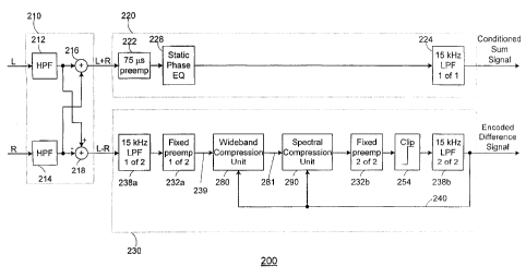
17 Detailed Description of the Drawings
18 Figure 3 is a block diagram of one embodiment of a digital BTSC encoder
19 200 constructed according to the invention. Digital encoder 200 is
constructed to
provide performance that is functionally equivalent to the performance of
21 idealized encoder 100 (shown in Figure 1). As with idealized encoder 100,
22 digital encoder 200 receives the left and right channel audio input signals
and
23 generates therefrom the conditioned sum signal and the encoded difference
signal,
24 however, in digital encoder 200 these input and output signals are
digitally
sampled signals rather than continuous analog signals.
26 The choice of sampling frequency fs for the left and right channel audio
27 input signals significantly affects the design of digital encoder 200. In
the
28 preferred embodiments, the sampling frequency fs is chosen to be an integer
29 multiple of the pilot frequency fH, so that fs=NfH where N is an integer,
and in
the most preferred embodiments, N is selected to be greater than or equal to
31 three. It is important for encoder 200 to insure that the conditioned sum
and
32 encoded difference signals do not contain enough energy at the pilot
frequency fH
13
CA 02255925 1998-11-13
WO 97/47102 PCT/US97/09493
1 to interfere with the pilot tone that is included in the composite signal.
As will
2 be discussed in greater detail below, it is therefore desirable for at least
some of
3 the filters in digital encoder 200 to provide an exceptionally large degree
of
4 attenuation at the pilot frequency fH, and this choice of sampling frequency
fS
simplifies the design of such filters.
6 Digital encoder 200 includes an input section 210, a sum channel
7 processing section 220 and a difference channel processing section 230.
Rather
8 than simply implementing the difference channel processing section 230 using
9 digital technology, all three sections 210, 220, 230 are implemented
entirely using
digital technology. Many of the individual components in digital encoder 200
11 respectively correspond to individual components in idealized encoder 100.
In
12 general, the components of digital encoder 200 have been selected so that
their
13 amplitude responses closely match the respective amplitude responses of
their
14 corresponding components in encoder 100. This often results in there being
a
relatively large difference between the phase responses of corresponding
16 components. According to one aspect of the present invention, means are
17 provided in digital encoder 200 for compensating for or nullifying these
phase
18 differences, or phase errors. As those skilled in the art will appreciate,
relatively
19 small phase errors in the difference channel processing section 230 may be
compensated for by introducing similar phase errors in the sum channel
21 processing section 220, and implementing the sum channel processing section
22 using digital technology simplifies the introduction of such desired
compensating
23 phase errors.
24 The input section 210 of encoder 200 includes two high pass filters 212,
214, and two signal adders 216, 218. The left channel digital audio input
signal
26 L is applied to the input of high pass filter 212, the latter generating
therefrom an
27 output signal that is applied to positive input terminals of adders 216,
218. The
28 right channel audio input signal R is applied to the input of high pass
filter 214
29 which generates therefrom an output signal that is applied to a positive
input
terminal of adder 216 and to a negative input terminal of adder 218. Adder 216
31 generates a sum signal (indicated in Figure 3 as "L+R") by summing the
output
32 signals generated by filters 212 and 214. Adder 2I8 generates a difference
signal
14
CA 02255925 1998-11-13
WO 97/47102 PCTIUS97/09493 -
1 (indicated in Figure 3 as "L-R") by subtracting the output signal generated
by
2 filter 214 from the output signal generated by filter 212. Input section 210
is
3 therefore similar to input section 110 (shown in Figure 1) however, section
2I0
4 additionally includes the two high pass filters 212, 214 and generates
digital sum
and difference signals.
6 High pass filters 212, 214 preferably have substantially identical responses
7 and preferably remove D.C. components from the left and right channel audio
8 input signals. As will be discussed in greater detail below, this D.C.
removal
9 prevents encoder 200 from exhibiting a behavior referred to as "ticking" .
Since
the audio information content of the left and right channel audio input
signals of
11 interest is considered to be within a frequency band between 50 Hz and
15,000
12 Hz, removal of D.C. components does not interfere with the transmission of
the
13 information content of the audio signals. Filters 212, 214, therefore,
preferably
14 have a cutoff frequency below 50 Hz, and more preferably have a cutoff
frequency below 10 Hz so that they will not remove any audio information
16 contained in the audio input signals. Filters 212, 214 also preferably have
a flat
17 magnitude response in their passband. In one preferred embodiment, filters
212,
18 214 are implemented as first order infinite impulse response (IIR) filters,
each
19 having a transfer function H(z) given by the formula shown in the following
Equation ( 1 ) .
-i
21 H(Z)= 1!Z (1)
1 +a lz -i
22 Referring again to Figure 3, the sum channel processing section 220
23 receives the sum signal and generates therefrom the conditioned sum signal.
In
24 particular, the sum signal is applied to a 75 ~.s preemphasis filter 222.
The filter
222 in turn generates an output signal that is applied to a static phase
26 equalization filter 228. The filter 228 generates an output signal that is
applied to
27 a low pass filter 224 of section 220 which in turn generates the
conditioned sum
28 signal.
29 The 75 ~,s preemphasis filter 222 provides signal processing that is
partially analogous to the filter 122 (shown in Figure 1) of idealized encoder
100.
CA 02255925 1998-11-13
WO 97/47102 PCT/US97/09493 -
1 The amplitude response of filter 222 is preferably selected to closely match
that
2 of filter 122. As will be discussed further below, means are preferably
provided
3 in difference channel processing section 230 for compensation for any
differences
4 in the phase responses of filters 222 and 122. In one preferred embodiment,
S filter 222 is implemented as a first order IIR filter having a transfer
function H(z)
6 that is described by the formula shown in the following Equation (2).
b+bz-1
7 H(z)= ° ' (2)
1+alz-i
8 Static phase equalization filter 228 performs processing that is not
directly
9 analogous to any of the components in idealized encoder 100 (shown in Figure
1).
As will be discussed in greater detail below, static phase equalization filter
228 is
11 used to introduce phase errors that compensate for phase errors introduced
by
12 difference processing section 230. Briefly, static phase equalization
filter 228 is
13 preferably an "all-pass" filter having a relatively flat amplitude response
and a
14 selected phase response. In one preferred embodiment, filter 228 is
implemented
as a first order IIR filter having a transfer function H(z) that is described
by the
16 formula shown in the following Equation (3).
17 H(z)= a°+z _1 (3)
1+a°z
18 Low pass filter 224 provides processing that is partially analogous to
19 bandlimiter 124 (shown in Figure 1) of encoder 100. Low pass filter 224
preferably provides a flat amplitude response in a pass band of zero to 15 kHz
21 and a relatively sharp cutoff above lSkHz. Filter 224 also preferably
provides an
22 exceptionally large degree of attenuation at the frequency fH of the pilot
tone (i. e. ,
23 15,734 Hz). By providing this exceptionally large degree of attenuation,
filter
24 224 insures that the conditioned sum signal does not include enough energy
at the
pilot frequency fH to interfere with the pilot tone used in the composite
signal.
26 As discussed above, selecting the sampling frequency fs to be equal to an
integer
27 multiple of the pilot frequency fH simplifies the design of a filter that
provides an
28 exceptionally large degree of attenuation at the pilot frequency and
therefore
29 simplifies the design of filter 224. Filter 224 preferably has a null at
the pilot
16
CA 02255925 1998-11-13
WO 97/47102 PCT/US97/09493
1 frequency fH and preferably provides at Least 70 dB of attenuation for all
2 frequencies from the pilot frequency fH up to one-half the sample rate.
3 Figure 4A is a block diagram illustrating one preferred embodiment of low
4 pass filter 224. As shown in Figure 4A, filter 224 may be implemented by
cascading five filter sections 310, 312, 314, 316, 318. In one preferred
6 embodiment, all five filter sections 310, 312, 314, 316, 318 are each
7 implemented as a second order IIR filter having transfer functions H(z)
which are
8 described by the formula shown in the following Equation (4).
9 H(zO b°+blz 1+bzZ z (4)
1 +a lz -i+azz -z
So in the embodiment shown in Fig. 4A, filter 224 is tenth order IIR filter.
11 Referring again to Figure 3, the difference channel processing section 230
12 receives the difference signal and generates therefrom the encoded
difference
13 signal. The difference signal is applied to a low pass filter 238a which
generates
14 therefrom an output signal that is applied to a fixed preemphasis filter
232a. The
latter generates an output signal that is applied via line 239 to an input
terminal of
16 a wideband compression unit 280, and the encoded difference signal is
applied via
17 feedback line 240 to a detector terminal of wideband compression unit 280.
The
18 latter generates an output signal that is applied via line 281 to an input
terminal of
19 a spectral compression unit 290, and the encoded difference signal is also
applied
via feedback line 240 to a detector terminal of unit 290. The latter generates
an
21 output signal that is applied to a fixed preemphasis filter 232b which in
turn
22 generates an output signal that is applied to a clipper 254. Clipper 254
generates
23 an output signal that is applied to a low pass filter 238b which in turn
generates
24 the encoded difference signal.
Low pass filters 238a, 238b, together form a low pass filter 238 that
26 performs processing that is partially analogous to the bandlimiter portion
of
27 overmodulation protector and bandlimiter 138 (shown in Figure 1) of
idealized
28 encoder 100. Preferably, filter 238 is implemented so that it is
substantially
29 identical to low pass filter 224, which is used in the sum channel
processing
section 220. Any phase errors introduced into the encoded difference signal by
17
CA 02255925 1998-11-13
WO 97/47102 PCT/US97/09493
1 filter 238 are therefore compensated by balancing phase errors that are
introduced
2 into the conditioned sum signal by filter 224. Filter 238 is preferably
split into
3 two sections 238a, 238b as shown for reasons which will be discussed in
greater
4 detail below, and filter 238a preferably has a null at the pilot frequency
fH.
Figures 4B-C are block diagrams illustrating one preferred embodiment of
6 the respective filters 238a and 238b. As shown in Figure 4B, filter 238a may
be
7 implemented by cascading three filter sections 310, 314, 318 that are
identical to
8 three of the filter sections used in filter 224 (shown in Figure 4A), and as
shown
9 in Figure 4C, filter 238b may be implemented by cascading two filter
sections
312, 316 that are identical to the two remaining sections used in filter 224.
11 Fixed preemphasis filters 232a, 232b (shown in Figure 3) together form a
12 fixed preemphasis filter 232 that performs processing that is partially
analogous to
13 filter 132 (shown in Figure 1) of idealized encoder 100. The amplitude
response
14 of filter 232 is preferably selected to closely match the amplitude
response of
filter 132. In one embodiment, the phase responses of filters 232 and 132 are
16 significantly different, and as will be discussed in greater detail below,
the
17 resulting phase errors are compensated for by filters 222 and 228 in the
sum
18 channel processing section 220. Filter 232 is preferably split into two
sections
19 232a, 232b as shown for reasons that will be discussed below. In one
preferred
embodiment, filters 232a, 232b are each implemented as first order IIR filters
21 having transfer functions H(z) that are described by the formula shown in
22 Equation (2). So in this embodiment filter 232 is a second order IIR
filter.
23 In one preferred embodiment, the difference between the phase responses
24 of filters 232b and 132a closely matches the difference between the phase
responses of filters 222 and 122. Therefore, the phase error introduced into
the
26 encoded difference signal by fixed preemphasis filter 232b is balanced by
the
27 phase error introduced into the conditioned sum signal by 75 ~,s
preemphasis filter
28 222. Further, in this embodiment, the phase response of static phase
equalization
29 filter 228 is selected to closely match the difference between the phase
responses
of fixed preemphasis filter 232a and filter 132b, so that any phase error
31 introduced into the encoded difference signal by filter 232a is balanced by
a
32 compensatory phase error in the conditioned sum signal that is introduced
by
18
CA 02255925 1998-11-13
WO 97!47102 PCT/US97/09493
1 static phase equalization filter 228. .
2 Clipper 254 performs processing that is partially analogous to the
3 overmodulation protection portion of overmodulation protector and
bandlimiter
4 138 (shown in Figure 1) used in idealized encoder 100. Briefly, clipper 254
is
implemented as a thresholding device, however, the operation of clipper 254
will
6 be discussed in greater detail below.
7 Wideband compression unit 280 and spectral compression unit 290
8 perform processing functions that are partially analogous to that of units
180 and
9 190, respectively, of idealized encoder 100 (shown in Figure 1). Briefly,
wideband compression unit 280 dynamically compresses the signal on line 239 as
11 a function of the overall energy level in the encoded difference signal and
spectral
12 compression unit 290 further compresses high frequency portions of the
signal on
13 line 281 as a function of high frequency energy in the encoded difference
signal.
14 Figure 5 shows a block diagram of a preferred embodiment of a digital
wideband compression unit 280. Unit 280 includes a digital signal multiplier
16 434, a digital signal multiplier 446, a wideband digital bandpass filter
448, a
17 digital RMS level detector 450, and a digital reciprocal generator 458.
These
18 components perform processing functions partially analogous to those
performed
19 by amplifier 134, amplifier 146, bandpass filter 148, RMS level detector
150, and
reciprocal generator 152, respectively, of idealized encoder 100 (shown in
Figure
21 1). The encoded difference signal is applied via feedback path 240 to an
input of
22 wideband digital bandpass filter 448 which generates therefrom an output
signal
23 that is applied to RMS level detector 450. The latter generates an output
signal
24 that is representative of the RMS value of the output signal generated by
filter
448 and applies this output signal via line 450a to reciprocal generator 458.
26 Reciprocal generator 458 then generates an output signal representative of
the
27 reciprocal of the signal on line 450a and applies this output signal via
line 458a to
28 multiplier 446. Digital signal multiplier 446 multiplies the signal on line
458a by
29 the value of the gain setting, Gain D, and thereby generates an output
signal that
is representative of D times the reciprocal of the RMS value and that is
applied
31 via line 446a to an input terminal of multiplier 434. The output signal
generated
32 by fixed preemphasis filter 232a is applied via line 239 to another input
terminal
19
CA 02255925 1998-11-13
WO 97/47102 PCT/US97/09493
1 of multiplier 434. Multiplier 434 multiplies the signal on line 239 by the
signal
2 on line 446a and thereby generates the output of wideband compression unit
280
3 which is applied via line 281 to the input of spectral compression unit 290.
4 Wideband digital bandpass filter 448 is designed to have an amplitude
S response that closely matches the amplitude response of bandpass filter 148
6 (shown in Figure 1). One preferred choice is to select filter 448 so that
the mean
7 square difference between its amplitude response and that of filter 148 are
8 minimized. In one embodiment, the phase response of filters 448 and 148 are
9 substantially different, but since the output signal of the RMS level
detector 450
is substantially insensitive to the phase of its input signal, these phase
differences
11 may be ignored. In one preferred embodiment, wideband bandpass filter 448
is
12 implemented as a second order IIR filter having a transfer function H(z)
that is
13 described by the formula shown in Equation (4).
14 RMS level detector 450 is designed to approximate the performance of
detector 150 which is used in idealized encoder 100 (shown in Figure 1).
16 Detector 450 includes a signal squaring device 452, a signal averaging
device
17 454, and a square root device 456. Squaring device 452 squares the signal
18 generated by bandpass filter 448 and applies this squared signal via line
452a to
19 averaging device 454. The latter computes a time weighted average of the
signal
on line 452a and applies the average via line 454a to square root device 456.
21 Square root device 456 calculates the square root of the signal on line
454a and
22 thereby generates a signal on line 450a representative of the RMS value of
the
23 output signal generated by wideband digital bandpass filter 448.
24 Averaging device 454 includes a digital signal multiplier 460, a digital
signal adder 462, a digital signal multiplier 464, and a delay register 465.
The
26 output signal generated by squaring device 452 is applied via line 452a to
one
27 input of multiplier 460 which generates an output signal by scaling the
signal on
28 line 452a by a constant a. The scaled output signal generated by multiplier
460
29 is applied to one input of adder 462 and an output signal generated by
delay
register 465 is applied to the other input of adder 462. Adder 462 generates
an
31 output signal by summing the signals present at its two inputs, and this
summed
32 signal is the output signal of averaging device 454 and is applied to
square root
,, ,
CA 02255925 1998-11-13
WO 97/47102 PCT/US97/09493
1 device 456 via line 454a. This summed signal is also applied to one input of
2 multiplier 464 which generates an output signal by scaling the summed signal
by
3 the constant (1-a). The output signal generated by multiplier 464 is applied
to
4 an input of delay register 465. Those skilled in the art will appreciate
that
averager 454 is a recursive filter and implements a digital averaging function
that
6 is described by the recursive formula shown in the following Equation (5).
7
8 y(n)=~'(n)+(1-a)Y(n-1)
9
in which y(n) represents the current digital sample of the signal output by
11 averager 454 on line 454a, y(n-1) represents the previous digital sample of
the
12 signal output by averager 454 on line 454a, and x(n) represents the current
digital
13 sample of the signal output by squaring device 452 on line 452a. Those
skilled in
14 the art will appreciate that averager 454 provides a digital approximation
of the
analog averaging function defined in the BTSC standard and implemented by
16 RMS level detector 150 (shown in Figure 1) of idealized encoder 100. The
17 constant a is preferably chosen so that the time constant of RMS level
detector
18 450 closely approximates the corresponding time constant specified in the
BTSC
19 standard for RMS level detector 150.
Digital square root device 456 and digital reciprocal generator 458 are
21 shown in Figure 5 as two separate components, however, those skilled in the
art
22 will appreciate that these two components may be implemented using a single
23 device that generates an output signal representative of the reciprocal of
the
24 square root of its input signal. Such a device may be implemented for
example
as a memory look up table (LUT), or alternatively may be implemented using
26 processing components that calculate a Taylor series polynomial
approximation of
27 the inverse square root function.
28 Figure 6 shows a block diagram of a preferred embodiment of spectral
29 compression unit 290. Unit 290 includes a variable preemphasis/deemphasis
unit
(hereinafter referred to as the "variable emphasis unit") 536, a signal
multiplier
31 540, a spectral band pass filter 542, and an RMS level detector 544, and
these
32 components provide processing which is partially analogous to that of
variable
21
CA 02255925 1998-11-13
WO 97/47102 PCT/US97/09493
1 emphasis filter 136, amplifier 140, .bandpass filter 142, and RMS level
detector
2 144, respectively, of idealized encoder 100 (shown in Figure 1). The encoded
3 difference signal is applied via feedback line 240 to an input of signal
multiplier
4 540 which generates an output signal by multiplying the encoded difference
signal
by the fixed gain setting value of Gain C. The amplified output signal
generated
6 by signal multiplier 540 is applied to spectral bandpass filter 542 which
generates
7 an output signal that is applied to RMS level detector 544. The latter
generates
8 an output signal that is applied via line 544a to a control terminal of
variable
9 emphasis unit 536, and the output signal generated by wideband compressor
unit
280 is applied via line 281 to an input terminal of unit 536. The latter
11 dynamically varies the frequency response applied to the signal on line 281
12 according to a function of the signal on line 544a, the latter signal being
a
13 function of the signal energy of the encoded difference signal vyithin the
14 frequency band passed by spectral band pass filter 542. The output signal
of unit
290, which is generated by unit 536 and is applied to the input of fixed
16 preemphasis filter 232b, is thus dynamically compressed a greater amount in
the
17 high frequency portions of the signal than in the remainder of the spectrum
of
18 interest.
19 Spectral bandpass filter 542 is designed to have an amplitude response that
closely matches the amplitude response of bandpass filter 142 (shown in Figure
1 )
21 of idealized encoder 100. As with filter 448 (shown in Figure 5), one
preferred
22 choice is to select filter 542 so that the difference between its RMS
amplitude
23 response and that of filter 142 are minimized. In one embodiment, the phase
24 response of filters 542 and 142 are substantially different, but since the
RMS
output of RMS level detector 544 is substantially insensitive to the phase of
the
26 input to the detector, these phase differences may be ignored. In one
preferred
27 embodiment, spectral bandpass filter 542 is implemented as a cascade of
three
28 second order IIR filter sections 542a, 542b, 542c (as shown in Figure 6)
each
29 having a transfer function H(z) that is described by the formula shown in
Equation {4).
31 RMS level detector 544 is designed to approximate the performance of
32 detector 144 which is used in idealized encoder 100 (shown in Figure 1).
22
CA 02255925 1998-11-13
WO 97/47102 PCT/US97/09493
1 Detector 544 includes a signal squaring device 552, a signal averaging
device
2 554, and a square root device 556. Squaring device 552 squares the signal
3 generated by spectral bandpass filter 542 and applies this squared signal
via line
4 552a to averaging device 554. The latter functions similarly to averaging
device
454 (shown in Figure 5) which is used in the wideband compression unit 280,
6 although device 554 preferably uses a constant /3 different from the
constant a.
7 The behavior of averaging device 554 is of course also described by Equation
(5)
8 when /3 is substituted for a. The constant ~3 is preferably selected for
device 554
9 so that the time constant of RMS level detector 544 closely approximates the
corresponding time constant specified by the BTSC standard for RMS level
11 detector 144 (shown in Figure 1). Averaging device 554 computes a time
12 weighted average of the signal on line 552a and applies the average to
square root
13 device 556 via line 554a. Square root device 556 calculates the square root
of the
14 signal on line 554a and thereby generates a signal on line 544a as a
function of
the RMS value of the output signal generated by spectral bandpass filter 542.
16 The signal on line 544a is applied to the control terminal of variable
17 emphasis unit 536. Variable emphasis unit 536 performs processing that is
18 partially analogous to filter 136 (shown in Figure 1) of idealized encoder
100. As
19 defined by the BTSC standard, filter 136 has amplitude and phase responses
that
vary as a function of the output signal generated by RMS level detector 144.
One
21 preferred way to implement unit 536 so that it has similar variable
responses is to
22 use a digital filter having variable coefficients that determine its
transfer function
23 and to select the value of the coefficients during any given sample period,
or
24 group of sample periods, based on the value of the signal on line 544a.
Figure 6 shows one embodiment of variable emphasis unit 536 which
26 includes a logarithmic generator 558, a variable emphasis filter 560, and a
look
27 up table LUT 562. The output signal generated by RMS level detector 544 is
28 applied via line 544a to logarithmic generator 558. The latter generates a
signal
29 on line 558a that is representative of the logarithm of the signal on line
544a and
applies this signal to LUT 562. LUT 562 generates an output signal selected
31 from the LUT and representative of filter coefficients to be used by
variable
32 emphasis filter 560. The coefficients thus generated by LUT 562 are applied
via
23
CA 02255925 1998-11-13
WO 97/47102 PCT/US97/09493
1 line 562a to a coefficient selection terminal of variable emphasis filter
560. The
2 output signal generated by wideband compression unit 280 is applied to an
input
3 terminal of variable emphasis filter 560 via line 281. Variable emphasis
filter
4 560 generates the output signal of spectral compression unit 290 which is
applied
to the input of fixed preemphasis filter 232b.
6 Variable emphasis filter 560 is designed to have a variable amplitude
7 response that closely matches the variable amplitude response of filter 136
(shown
8 in Figure 1) of idealized encoder 100. Variable emphasis filter 560 provides
a
9 similar variable response by using a variable coefficient transfer function
(i.e., the
coefficients of the transfer function H(z) of filter 560 are variable) and by
11 allowing LUT 562 to select the value of the coefficients during intervals
based on
12 the sample period. As will be described in greater detail below, LUT 562
stores
13 the values of the filter coefficients used by filter 560, and during each
sample
14 period, or during any selected group of sample periods, LUT 562 selects a
set of
filter coefficients as a function of the output signal generated by
logarithmic
16 generator 558 on line 558a. In one preferred embodiment, variable emphasis
17 filter 560 is implemented as a first order IIR filter having a transfer
function H(z)
18 that is described by the formula shown in the following Equation (6).
bo+b iz _ i
19 H(z)= (6)
1+a lz -~
in which the filter coefficients bo, b,, and a, are variables that are
selected by
21 LUT 562. Methods of selecting the values for the filter coefficients used
by filter
22 560 as well as by the other filters of encoder 200 will be discussed below.
23 In Figure 6, logarithmic generator 558 and square root device 556 are
24 shown, for convenience, as two separate components. However, those skilled
in
the art will appreciate that these two components may be implemented using a
26 single device, such as a LUT, or alternatively using processing components
that
27 calculate a Tayler series polynomial approximation of the logarithm of the
signal
28 on line 554a and by then dividing this value by two. Similarly, in
alternative
29 implementations, the functions performed by logarithmic generator 558,
square
root device 556, and LUT 562 may be incorporated into a single device.
24
T f " ~ ~ ,
CA 02255925 1998-11-13
WO 97/47102 PCT/C1S97/09493
1 As stated above, high pass filters 212, 214 (shown in Figure 3) are useful
2 in blocking DC components so as to prevent encoder 200 from exhibiting a
3 behavior known as "ticking" . In the context of a stereophonic encoder,
ticking
4 refers to relatively low frequency oscillatory behavior of the encoder
caused when
there is no signal present at the left and right channel audio inputs. The
desired
6 behavior of a stereophonic system when there is no signal present at the
audio
7 inputs is to remain silent; however, an encoder connected through a decoder
to
8 loudspeakers and exhibiting ticking causes the loudspeakers to emit an
audible
9 sound, referred to as a "tick" , with a somewhat regular period that is
partially
dependent on the time constant of the RMS level detector in the wideband
11 compressor. More particularly, in encoder 200, when only very low level
signals
12 are present at the audio inputs, and when there is a D.C. component, or an
13 offset, present in the signal on line 239, wideband compression unit 280
tends to
14 behave in an unstable fashion that causes ticking.
Consider the case where only a low level audio signal is present on line
16 239. In such a case, the output of RMS level detector 450 on line 450a
becomes
17 very small, which in turn causes the gain of multiplier 434 to become very
large.
18 If such a low level audio signal on line 239 is constant in its amplitude,
the
19 wideband compression unit 280 reaches a steady-state condition after some
time
(determined by the time constant a applied to multiplier 460), because the
21 encoded difference signal is fed back on line 240 to the wideband
compression
22 unit 280. Because the feedback is arranged to be negative, when the audio
signal
23 on line 239 increases in its amplitude, the signal on line 450a increases,
which in
24 turn causes the gain of multiplier 434 to decrease. When the audio signal
on line
239 decreases in its amplitude, the signal on line 450a decreases, which in
turn
26 causes the gain of multiplier 434 to increase.
27 However, should there be a significant do signal present on line 239 in
28 addition to a low level audio signal, the do signal is blocked from the
feedback
29 process by the action of wideband bandpass filter 448, which has zero
response to
do signals. In particular, any do present in the encoded difference signal at
line
31 240 is blocked by filter 448, and is not sensed by RMS level detector 450.
Any
32 do signal present on line 239 will be amplified by multiplier 434 along
with any
CA 02255925 1998-11-13
WO 97/47102 PCT/US97/09493
1 audio signal present on line 239, but the amplification factor or gain will
be
2 determined only by the audio signal amplitude as sensed by RMS level
detector
3 450 after filtering by filter 448.
4 As noted above, whenever the amplitude of the audio signal on line 239
varies, the gain of multiplier 434 varies inversely. During such variations in
6 gain, any do present on line 239 will also be subjected to variable
amplification,
7 in effect modulating the do signal, thereby producing an ac signal. In this
fashion
8 such do signals may be modulated so as to create significant audio-band
signals
9 which will not be rejected by filter 448, and are therefore sensed by
detector 450.
When the audio signal on line 239 is small compared to the do on line 239,
small
11 variations in the audio signal level, which cause changes in the gain of
amplifier
12 434, can cause a large change in the do level (which amount to an ac
signal) at
13 line 281 through this modulation process. The ac signal produced tends to
14 increase the overall signal which passes through filter 448, regardless of
whether
the audio signal variation that gave rise to the ac signal was an increase or
16 decrease in signal level. In particular, should the level of the audio
signal on line
17 239 decrease, the negative feedback process normally increases the gain of
18 multiplier 434. However, if a sufficient do signal is present in line 239,
a
19 decrease in audio signal on line 239 can cause an increase in the signal
sensed by
detector 450, forcing the gain of multiplier 434 to decrease. In this fashion,
the
21 negative feedback process is reversed, and the feedback becomes positive.
22 Such positive feedback will only persist so long as the modulated do signal
23 at line 281 is sufficiently large compared to any audio signal present on
line 281,
24 when weighted by the response of all the filters and signal modifiers
between line
281 and the output of filter 448. Once the gain of multiplier 434 decreases
26 sufficiently such that the modulated do signal in line 281 no longer
provides a
27 significant input to detector 450, the feedback reverts to its normal
negative
28 sense. In accordance with the time constant of detector 450, the system
will re-
29 acquire an appropriate gain level based on the level of the audio signal in
line
239. But, if sufficient do remains in the signal in line 239, the cycle will
repeat
31 itself once the gain of multiplier 434 increases sufficiently. During each
such
32 period of positive feedback, a sharp change in the do level of line 281 is
26
CA 02255925 1998-11-13
WO 97/47102 PCTIUS97/09493
1 produced. This change is audible, and sounds somewhat similar to the 'tick'
of a
2 clock. Since such do changes will occur with some regularity, based on the
time
3 constant of detector 450, the phenomenon is often referred to as 'ticking' .
4 One method of preventing ticking is to remove any do components present
in the input signal to encoder 200. This is accomplished by high pass filters
212
6 and 214. Further, high pass filters 212 and 214 help to maximize the dynamic
7 range of encoder 200 by removing do components which otherwise may use up
8 valuable dynamic range. As stated above and as shown in Figure 3, low pass
9 filter 238 is preferably implemented as two filters 238a and 238b. Splitting
filter
238 in this fashion provides several advantages. If filter 238a were
eliminated,
11 and the entire filter 238 were located after clipper 254 (i.e., in the
location of
12 filter 238b) then any components above 15 kHz on the audio input signals
may
13 cause instability in the wideband compression unit 280 similar to the above-
14 described ticking behavior. This occurs because any signal components above
15
kHz on line 239 will be amplified by multiplier 434 (shown in Figure 5) and
16 because such components will not be sensed by RMS level detector 450 since
17 such components are filtered out by the low pass filter following clipper
254
18 (shown in Figure 3). Since detector 450 increases the gain of multiplier
434
19 when it senses the absence of a signal, the gain of multiplier 434 can
become
relatively large when the signal on line 239 consists of little audio signal
(under
21 lSkHz) information, but significant high-frequency (over lSkHz)
information.
22 Multiplier 434 then amplifies the high-frequency information, which can
generate
23 large signals that are likely to be clipped by components in processing
section
24 230. This clipping can produce harmonics which may alias to low frequencies
that will be sensed by RMS level detector 450 causing the system to tick as
2b described previously. Alternatively, if filter 238b were eliminated and the
entire
27 filter 238 were located before fixed preemphasis filter 232a (i.e., in the
location
28 of filter 238a) then high frequency artifacts generated by clipper 254
would be
29 included in the encoded difference signal and could interfere with the
pilot tone in
the composite signal. Therefore, splitting filter 238 as shown provides an
optimal
31 arrangement whereby filter 238a prevents ticking in compression unit 280
and
32 filter 238b filters high frequency artifacts that may be generated by
clipper 254.
27
CA 02255925 1998-11-13
WO 97/47102 PCT/US97/09493
1 Fixed preemphasis filter 232 is also preferably split into two filters 232a,
2 232b as shown in Figure 3. Filter 232 typically requires relatively large
gain at
3 high frequencies, as is specified in the BTSC standard, and using only a
single
4 section to implement filter 232 increases the likelihood of filter 232
causing
clipping. It is advantageous to apply some of the gain of filter 232 on the
input
6 side of wideband compression unit 280 (with filter 232a) and to apply some
of the
7 gain of filter 232 on the output side of wideband compression unit 280 (with
filter
8 232b). Since unit 280 normally compresses its input signal, distributing the
gain
9 of filter 232 around the compression provided by unit 280 decreases that the
likelihood that the gain of filter 232 will cause an overflow condition.
11 To minimize size, power consumption, and cost, encoder 200 is preferably
12 implemented using a single digital signal processing chip. Encoder 200 has
been
13 successfully implemented using one of the well known Motorola DSP 56002
14 digital signal processing chips (this implementation shall be referred to
hereinafter
as the "DSP Embodiment"). The Motorola DSP 56002 is a fixed point twenty-
16 four bit chip, however, other types of processing chips, such as floating
point
17 chips, or fixed point chips having other word lengths, could of course be
used.
18 The DSP Embodiment of encoder 200, uses a sampling frequency fs that is
equal
19 to three times the pilot frequency fH (i.e., fs = 47202 Hz). The following
Table
1 lists all of the filter coefficients used in the DSP Embodiment of encoder
200
21 except those used in variable emphasis filter 560.
22 TABLE 1
23 Low Pass Filter (Section Low Pass Filter (Section #2)
24 #1) 310 312
(Equation 4) (Equation 4)
bo=0.18783270 bo=0.44892888
26 bl=0.36310206 bl=0.70268024
27 b2=0.18783270 b2=0.44892888
28 a, =-0.388832539 a, =0.12638618
29 a2=0.12709286 a2=0.47415181
Low Pass Filter (Section Low Pass Filter (Section #4)
31 #3) 314 316
(Equation 4) (Equation 4)
28
CA 02255925 1998-11-13
WO 97/47102 PCT/US97/09493
1 bo=0.70674027 ~ bo=0.85733126
2 b, =0.87637648 b, =0.91505047
3 bz=0.70674027 bz=0.85733126
4 a, =0.53702472 a, =0.74320197
az=0.75298490 az=0.89832289
6 Low Pass Filter (Section Wideband Bandpass Filter 448
7 #5) 318 (Equation 4)
(Equation 4)
8 bo=0.92737972 bo=-0.02854672
9 b, =0.92729649 b, =-0.18789051
b2=0.92737972 b2=0.21643723
11 a, =0.82951974 a, =-1.75073141
12 a2=0.97259237 a2=0.75188028
13 Fixed Preemphasis Filter Fixed Preemphasis Filter 238b
14 238a (Equation 2)
(Equation 2)
bo=9.50682180 bo=4.357528
16 b, =-9.00385663 b, =-3.24843271
17 a, =-0.497064357 a, =0.10881833
18 Spectral Bandpass Filter Spectral Bandpass Filter
19 (Section #1) 542a (Section #2) 542b
(Equation 4) (Equation 4)
21 ba=0.646517841 bo=0.850281278
22 b, =0.649137616 b, =-0. 850247036
23 bz=0.0 bz=0.0
24 a, =0.557821757 a, =-0.602159890
a2=0.0 az=0.0
26 Spectral Bandpass Filter Static Phase Equalization Filter
27 (Section #3) 542c 224
28 (Equation 4) (Equation 3)
29 bo=0.597678418 a~,=0.9029
29
CA 02255925 1998-11-13
WO 97/47102 PCT/US97/09493
1 b, =-1.195357770
2 bZ=0.597679348
3 a, =-0.776566094
4 a2=0.352824276
75 acs preemphasis filter High Pass Filters 212, 214
222
6 (Equation 2) (Equation 1 )
7 bo=4.57030583 a1=-0.999
8 b1=-3.43823487
9 a, =0.131778883
11 In the DSP Embodiment of
encoder 200 the value of
the constant a that is
12
used
by
averager
454
(shown
in
Figure
5)
in
wideband
compression
unit
280
is
13 set equal to 0.0006093973517,
and the value of the constant
/3 that is used by
14 averager 554 (shown in Figure
6) in spectral compression
unit 290 is set equal to
0.001825967. Further, the
values of Gain C and Gain
D used by amplifiers 540
16 and 446, respectively, in
the spectral and wideband
compression units are set
I7 equal to 0.5011872 and 0.08984625,
respectively, to insure
that the DSP
18 Embodiment of encoder 200
performs similarly to encoder
100.
19 Figure 7 shows a flow chart
700 that describes one
preferred method for
pre-calculating all the
sets of filter coefficients
used by variable emphasis
filter
21 560 (shown in Figure 6)
in the DSP Embodiment of
encoder 200. Prior to
22 operation of encoder 200,
all the sets of filter
coefficients used by filter
560 are
23 pre-calculated (e.g., by
a general purpose digital
computer) and are loaded
into
24 LUT 562. In the DSP Embodiment
of encoder 200, filter
560 has a transfer
function H(z) that is described
by Equation (6) so flow
chart 700 describes the
26 calculation of the coefficients
bo, b,, and a,. As specified
in the BTSC standard,
27 the transfer function of
S(f,b) of analog filter
136 (shown in Figure 1)
to which
28 filter 560 partially corresponds,
is described by the formula
shown in the
29 following Equation (7).
CA 02255925 1998-11-13
WO 97/47102 PCTIUS97/09493 -
F J(b+51 )
1+
1 S(f, b)= (b+1) (7)
~~~(1+51b)
1+
(b+1)
2 in which F is equal to 20.1 kHz.
3 The first step in flow chart 700 in an initialization step 710 during which
4 several variables are initialized. Specifically, the sampling frequency fs
is set
equal to 47202 Hz, and the period T is set equal to 1/fs. The variable W is a
b digital version of the variable F used in Equation (7) and is set equal to
x(20.1
7 kHz)/fs. The variable dBRANGE represents the desired signal range of the RMS
8 detectors in the spectral compression unit, and for the DSP Embodiment
9 dBRANGE is set equal to 72.25 dB. The variable dBRES relates to the
sensitivity of filter 560 to changes in the energy level of the encoded
difference
11 signal. In the DSP Embodiment of encoder 200, dBRES is set equal to 0.094
dB
12 so that filter 560 will use coefficients based on the value of the signal
on line
13 558a quantized to the nearest 0.094 dB. The variable N equals the total
number
14 of sets of filter coefficients used in filter 560 and N is calculated by
dividing the
sensitivity (dBRES) into the range (dBRANGE) and rounding to the nearest
16 integer. In the DSP Embodiment, N is equal to 768 although those skilled in
the
17 art will appreciate that this number can be changed which will vary the
sensitivity
18 or the range. In the DSP Embodiment, LUT 562 stores 769 sets of
coefficients
19 for filter 560, and of course if N is increased, a larger LUT will be used
to store
the extra sets of filter coefficients. Further, those skilled in the art will
21 appreciate that logarithmic generator 558 scales the signal on line 558a
and
22 thereby reduces the number of filter coefficient sets stored by LUT 562,
for a
23 given minimum quantization of the value of the signal on line 558a.
However, in
24 other embodiments, logarithmic generator 558 may be eliminated and LUT 562
may store a correspondingly larger number of filter coefficient sets. Finally,
the
26 variables Scale and Address are set equal to 32 and zero, respectively. The
31
CA 02255925 1998-11-13
WO 97/47102 PCT/US97/09493
1 variable Scale, which is only used in fixed point implementations, is
selected so
2 that all the filter coefficients have a value greater than or equal to
negative one
3 and less than one (where the filter coefficients are represented in twos
4 complement).
Following initialization step 710, a coefficient generation step 720 is
6 executed. During the first execution of step 720, variables bo(0), b,(0),
and a,(0)
7 are calculated which correspond to values of the coefficients bo, b,, and a~
that
8 are to be stored at address location zero of LUT 562. Following this
execution of
9 step 720, an incrementing step 730 is executed during which the value of the
variable Address is incremented. Following step 730 a comparison step is
11 executed during which the values of the variables Address and N are
compared.
12 If Address is less than or equal to N, then steps 720, 730, and 740 are
reexecuted
13 iteratively so that values of the coefficients bo, b,, and a, are
calculated for each
14 of the 769 addresses of LUT 562. When step 740 detects that the value of
Address is greater than N, then all 769 sets of coefficients have been
calculated
16 and execution of flow chart 700 proceeds to a concluding step 750.
17 In coefficient generation step 720, the variable dBFS corresponds to the
18 output of logarithmic generator 558. As the value of the variable Address
ranges
19 from zero to 769, the value of dBFS ranges from about -72.25 to zero dB
corresponding to the signal range of about 72.25 dB provided by the DSP
21 Embodiment of encoder 200 (where zero dB corresponds to the full
modulation).
22 The variable RMSd corresponds to the output of the analog RMS level
detector
23 144 (shown in Figure 1), and as the variable Address ranges from zero to
769,
24 the value of RMSd ranges from about -36 to 36 dB corresponding to the
signal
range of 72 dB provided by typical prior art analog BTSC encoders. The
26 variable RMSb is a linear version of the variable RMSd, and RMSb
corresponds
27 to the variable b in the transfer function S(f,b) described in Equation
(7). The
28 variables K1 and K2 correspond to the (b+51)/(b+1) and the (Slb+1)/(b+1)
29 terms, respectively, in Equation (7). The coefficients bo, b~, and a~ are
calculated as shown in step 720 using the variables Kl, K2, W, and Scale.
31 Figure 8A shows a block diagram that illustrates one method of using the
32 DSP Embodiment in an analog system, and in Figure 8A, all components that
are
32
T I ~ ~ . i
CA 02255925 1998-11-13
WO 97/47102 PCT/US97109493
1 implemented in the 56002 integrated circuit are indicated at 200a. The
analog
2 system supplies analog left and right channel audio input signals (shown in
Figure
3 8A as "L" and "R", respectively) and these signals are applied to the inputs
of
4 sixteen bit analog-to-digital converters 810 and 812, respectively.
Converters
810, 812 sample their analog input signals using a sampling frequency fs that
is
6 equal to 47,202 Hz (i.e., 3fH) and converters 810, 812 thereby generate
sequences
7 of sixteen bit digital samples that are representative of the left and right
channel
8 audio input signals, respectively. The signals generated by converters 810
and
9 812 are applied to encoder 200a where they are received by modules 292 and
294, respectively. Modules 292, 294 are "divide by sixteen" modules (which
11 divide the amplitude of their inputs by a factor of 16) and therefore
generate
12 output signals that are equal to their input signals divided by sixteen.
Since
13 division by any power of two is easily accomplished in a digital system by
using
14 a shift register, modules 292, 294 are implemented as shift registers that
shift
their inputs by four binary places.
16 As stated above, the 56002 chip is a fixed point twenty-four bit processor,
17 and the samples applied to the chip by converters 810, 812 are in twos
18 complement representation. Modules 292, 294 divide the samples generated by
19 converters 810, 812 by sixteen and thereby place each of the samples in the
middle of a twenty-four bit word. So in every sample generated by modules 292,
21 294, the four most significant bits are sign bits and the four least
significant bits
22 are zeros, and the sixteen bits in the middle of the word correspond to one
23 sample generated by one of the converters 810, 812. Padding each twenty-
four
24 bit word with sign bits at the high end and with zeros at the low end in
this
fashion preserves accuracy and allows intermediate signals generated by
encoder
26 200a to exceed sixteen bits without causing an error condition such as an
27 overflow.
28 In encoder 200a, each bit of the twenty-four bit word corresponds roughly
29 to 6dB of signal range, and therefore modules 292, 294 correspond to -24 dB
(i.e., negative 6 times 4) attenuators. If the analog input signals applied to
31 converters 810, 812 are considered for reference purposes as zero dB
signals,
32 then the signals generated by modules 292, 294 are attenuated by 24 dB.
33
CA 02255925 1998-11-13
WO 97/47102 PCT/US97/09493
1 Input section 210 receives the twenty-four bit words generated by modules
2 292, 294 and generates therefrom the sum signal that is applied to the sum
3 channel processing section 220. The output signal generated by sum channel
4 processing section 220 is applied to a "times 16 module" (which may be
considered as a 24 dB amplifier) 296. Module 296 thereby compensates for the -
6 24dB attenuators 292, 294 and brings the output of sum channel processing
7 section 220 back to 100% modulation (i.e., back to "full scale"). The output
8 signal generated by module 296 is applied to a sixteen bit digital-to-analog
9 converter 814 which in turn generates an analog conditioned sum signal.
Input section 210 also generates the difference signal that is applied to the
11 difference channel processing section 230. As stated above, as a result of
12 modules 292, 294, the difference signal may be considered as being
attenuated by
13 24 dB. In the DSP embodiment of encoder 200a, clipper 254 (shown in Figure
14 3) of the difference processing section 230 includes an 18 dB amplifier
(which is
implemented as a multiply by eight). That is, clipper 254 amplifies the signal
16 generated by fixed preemphasis filter 232b by 18 dB and then clips this
amplified
17 signal so that the output signal generated by clipper 254 will not exceed a
number
18 that is 6dB down from full modulation. The signal applied from clipper 254
to
19 low pass filter 238b therefore has one bit (or 6 dB) of "headroom", so
filter 238b
may generate an output signal that is 6 dB greater than its input signal
without
21 causing saturation. It is desirable to leave this one bit of headroom
because the
22 transient response of filter 238b includes some ringing that may cause it
to
23 temporarily generate an instantaneous output signal that is greater than
its
24 instantaneous input signal and the headroom thereby prevents any ringing in
filter
238b from causing a saturation condition. Referring again to Figure 8A, the
26 output signal generated by filter 238b is applied to a sixteen bit digital-
to-analog
27 converter 816 which in turn generates an output signal that is applied to a
6 dB
28 analog amplifier 820. Both D/A converters 814 and 816 are intended to be
29 complete converters, which include the well-known analog anti-image filters
as
part of their functionality. Anti-image filters are analog filters applied to
the
31 analog signal following digital to analog conversion which serve to
attenuate any
32 images of the desired signal which are mirrored about the sample frequency
and
34
CA 02255925 1998-11-13
WO 97/47102 PCT/US97/09493 -
1 multiples thereof. Converters 814 and 816 are assumed to be substantially
2 identical to one another, running at the same sample rate and containing
3 substantially the same anti-image filtering. Such converters are commonly
4 available in commercial embodiments, such as the Crystal Semiconductor
CS4328. Amplifier 820 amplifies its input signal by 6 dB and thereby brings
the
6 encoded difference signal back up to full scale. While Figure 8A shows
encoder
7 200a coupled to analog-to-digital converters 810, 812 for receiving analog
audio
8 signals, in digital systems converters 810, 812 may of course be eliminated
so
9 that encoder 200a receives the digital audio signals directly.
Figure 8B shows a block diagram of one preferred embodiment of a BTSC
11 encoder 200b constructed according to the invention and configured as part
of an
12 analog system. Encoder 200b is similar to encoder 200a, however, in encoder
13 200b module 296 amplifies its input signal by 18 dB (by multiplying by 8)
rather
14 than by 24 dB as in encoder 200a. The output signal generated by module 296
is
a scaled version of the conditioned sum signal and is shown in Figure 8B as S.
16 Also, encoder 200b includes a module 298 for amplifying the output signal
17 generated by difference channel processing section 230 by 6 dB (by
multiplying
18 by two). The output signal generated by module 298 is a scaled version of
the
19 encoded difference signal and is shown in Figure 8B as D. Further, encoder
200b includes a composite modulator 822 for receiving the signals S and D and
21 for generating therefrom a digital version of the composite signal. The
digital
22 composite signal generated by modulator 822 is applied to a digital-to-
analog
23 converter 818 the output of which is an analog version of the composite
signal.
24 D!A converter 818 is intended to be a complete converter which includes the
aforementioned analog anti-image filter as part of its functionality. Such
26 converters are commonly available in commercial embodiments, such as the
Burr-
27 Brown PCM1710. In the preferred embodiments, modules 292, 294, input
28 section 210, sum channel processing section 220, difference channel
processing
29 section 230, modules 296, 298, and composite modulator 822 are all
implemented
on a single digital signal processing chip.
31 Since the composite signal is generated as a digital signal in encoder
200b,
32 module 298 is included to bring the output signal generated by difference
channel
CA 02255925 1998-11-13
WO 97/47102 PCT/US97/09493
1 processing section 230 up to full scale rather than waiting until after
digital-to-
2 analog conversion and using an analog amplifier such as amplifier 820 as is
3 shown in Figure 8A. Also, since in the composite signal the conditioned sum
4 signal is used at 50 % modulation, module 296 only amplifies its input
signal by
18 dB so that the output signal generated by module 296 is at half the
amplitude
6 of the output signal generated by module 298.
7 Figure 9 shows a block diagram of one embodiment of composite
8 modulator 822. The latter receives the signals S and D and generates
therefrom a
9 digital version of the composite signal. Modulator 822 includes two
interpolators
910, 912, two digital low pass filters 914, 916, a digital signal multiplier
918,
11 and two digital signal adders 920, 922. The S and D signals are applied to
12 respective inputs of the interpolators 910 and 912. Interpolators 910, 912,
which
13 are alternatively referred to as "up-samplers" , interpolate a new sample
between
14 every two consecutive samples applied to their inputs, and thereby generate
output signals having twice the sampling frequency as the input signals S and
D.
16 The output signals generated by interpolators 910 and 912 are applied to
17 respective inputs of low pass filters 914 and 916. The latter remove images
18 introduced into the S and D signals by interpolators 910, 912. The filtered
output
19 signal generated by filter 916 is applied to one input of signal multiplier
918 and
a digital oscillating signal as a function of cos[4~(fH/fs)n] is applied to
the other
21 input of multiplier 918. Multiplier 918 thereby generates the amplitude
22 modulated, double-sideband, suppressed carrier version of the difference
signal
23 that is used in the composite signal. The output signal generated by
multiplier
24 918 is applied to one input of signal adder 920 and the filtered output
signal
generated by filter 914 is applied to the other input of signal adder 920. The
26 latter generates an output signal by summing the two signals present at its
inputs
27 and applies this signal to signal adder 922. A pilot tone signal that
oscillates as a
28 function of Acos[2~r(fH/fs)n] (where 'A' is a constant representative of 10
% of
29 full scale modulation) is applied to the other input of signal adder 922
which
generates the digital composite signal by summing the two signals present at
its
31 inputs.
32 Composite modulator 822 includes interpolators 910, 912 because the
36
CA 02255925 1998-11-13
WO 97!47102 PCT/US97/09493
1 highest frequency component in the. composite signal is slightly less than
3fH (as
2 is shown in Figure 2), and therefore the signals applied to the inputs of
signal
3 multiplier 918 and signal adder 920 should have sample rates at least as
large as
4 6fH to satisfy the Nyquist criteria. Because the sample rate at the output
of
composite modulator 822 is typically higher than the sample rate of either the
S
6 or D signals, D/A converter 818 must be capable of operating at such higher
7 sample rates. If the input signals S and D applied to composite modulator
822
8 have sample rates of 3fH some form of interpolation (such as that provided
by
9 interpolators 910, 912) should be provided to double the sample rate. Of
course,
if sufficiently high sample rates are used throughout encoder 200b then
11 interpolators 910, 912 and low pass filters 914, 916 may be eliminated from
12 modulator 822.
13 Figure 8C shows a block diagram of yet another embodiment of a BTSC
14 encoder 200c constructed according to the invention. Encoder 200c is
similar to
encoder 200b (shown in Figure 8B) however, in encoder 200c module 298 is
16 eliminated so that the signal generated by the difference channel
processing
17 section 230 is the signal D and is applied directly to composite modulator
822.
18 Further, in encoder 200c, module 296 amplifies its input signal by 12 dB
(by
19 multiplying by 4) rather than by 18 dB as is done in encoder 200b. So in
encoder 200c, the signals S and D are 6 dB down from the levels of those
signals
21 in encoder 200b. Composite modulator 822 therefore generates from these
22 signals a version of the composite signal that is attenuated by 6 dB. This
23 attenuated version of the composite signal is converted to an analog signal
by
24 digital-to-analog converter 818 and is then brought up to full scale by 6
dB analog
amplifier 820. As with encoder 200b, encoder 200c is preferably implemented
26 using a single digital signal processing chip.
27 The differences between encoders 200b and 200c represent design
28 tradeoffs. As those skilled in the art will appreciate, when converting a
digital
29 signal to an analog signal with a digital-to-analog converter, insuring
that the
digital signal is at full scale tends to minimize any loss of signal-to-noise
ratio
31 that might occur as a result of the conversion. Encoder 200b minimizes the
loss
32 of signal-to-noise ratio as a result of the operation of converter 818 by
using
37
CA 02255925 1998-11-13
WO 97/47102 PCTIUS97109493
1 modules 296, 298 to insure that the digital version of the composite signal
2 {generated by modulator 822) that is applied to converter 818 is at full
scale.
3 However, although converter 200b minimizes any loss of signal-to-noise ratio
that
4 might occur as a result of converter 818, encoder 200b also increases the
likelihood that clipping might occur in the composite signal. Since the
difference
6 channel processing section 230 uses the relatively large gain provided by
fixed
7 preemphasis filter 232 (shown in Figure 3), it is possible for some clipping
to
8 occur in the path of the encoded difference signal. Encoder 200b uses module
9 298 to bring the D signal up to full scale and this essentially eliminates
any
headroom from the signal path of the D signal and thereby increases the chance
11 that some clipping will occur. So encoder 200b minimizes the loss of any
signal-
12 to-noise ratio that occurs as a result of converter 818 at the cost of
increasing the
13 likelihood of clipping in the path of the encoded difference signal. In
contrast,
14 encoder 200c preserves headroom in the path of the encoded difference
signal and
thereby reduces the likelihood of clipping at the cost of increasing the loss
of
16 signal-to-noise ratio that occurs as a result of operation of converter
818.
17 Figure 8D shows a block diagram of yet another embodiment of a BTSC
18 encoder 200d constructed according to the invention. Encoder 200d is
similar to
19 encoder 200a (shown in Figure 8A) however, encoder 200d additionally
includes
a portion 822a of a composite modulator. Portion 822a includes two
interpolators
21 910, 912, two low pass filters 914, 916, digital signal multiplier 918 and
a digital
22 signal adder 930. The S signal generated by module 296 is applied to
23 interpolator 910 which "up-samples" the S signal and applies the up-sampled
24 signal to low pass filter 914. The latter filters this signal and applies
the filtered
signal to one input terminal of adder 930. A digital pilot tone having twice
the
26 normal amplitude {i.e., 2Acos2n(fH/fs)n) is applied to the other input
terminal of
27 adder 930 which generates an output signal by summing the two signals
present at
28 its input terminals. The D signal generated by difference channel
processing
29 section 230 is applied to interpolator 912 which generates an up-sampled
signal
that is applied to low pass filter 916. The latter filters this signal and
applies the
31 filtered signal to one terminal of multiplier 918. A signal oscillating
according to
32 cos4~r(fH/fs)n is applied to the other terminal of multiplier 918 which
generates an
38
CA 02255925 1998-11-13
WO 97/47102 PCT/US97/09493
1 output signal by multiplying the two signals present at its input terminals.
As
2 with encoders 200a-c, encoder 200d is preferably implemented using a single
3 digital signal processing chip.
4 Encoder 200d is preferably used in conjunction with two digital-to-analog
converters 932, 934, an analog -6 dB attenuator 936, an analog 6 dB amplifier
6 938, and an analog adder 940. The output signal generated by adder 930 is
7 applied to converter 932 which generates an analog signal that is applied to
8 attenuator 936. The output signal generated by multiplier 918 is applied to
9 converter 934 which generates an analog signal that is applied to amplifier
938.
The signals generated by attenuator 936 and amplifier 938 are applied to input
11 terminals of signal adder 940 which sums these signals to generate the
analog
12 composite signal. D/A converters 932 and 934 are intended to be complete
13 converters which include the aforementioned analog anti-image filters as
part of
14 their functionality. Converters 932 and 934 are assumed to be substantially
identical to one another, running at the same sample rate and containing
16 substantially the same anti-image filtering. Such converters are commonly
17 available in commercial embodiments, such as the Burr Brown PCM1710.
18 It is also possible to eliminate interpolator 910 and low pass filter 914
19 from Figure 8D, and run D/A converter 932 at a sample rate equal to that of
the
sum channel processing section 220. However, to do so is generally not
practical
21 because inexpensive, commonly available D/A converters are usually
available in
22 pairs housed within a single integrated circuit. Such paired D/A converters
23 naturally operate at the same sample rate. While it is possible to reduce
DSP
24 complexity by eliminating interpolator 910 and low pass filter 914 from
Figure
8D, doing so would also likely increase the cost and complexity of the overall
26 design because a simple stereo D/A converter could no longer be used for
both
27 DI A converters 932 and 934.
28 Encoder 200d represents one combination of the features of encoders 200b
29 and 200c. Encoder 200d uses module 296 to bring the S signal up to full
scale so
as to minimize any loss of signal-to-noise ratio that might occur as a result
of the
31 operation of converter 932. Encoder 200d also preserves 6 dB of headroom in
32 the signal path of the D signal and therefore reduces the likelihood of any
loss of
39
CA 02255925 1998-11-13
WO 97/47102 PCT/US97/09493
1 accuracy due to clipping. Although encoder 200d includes more components
than
2 either of encoders 200b and 200c, encoder 200d both minimizes loss of signal-
to-
3 noise ratio and the likelihood of clipping.
4 Figure 10 shows a block diagram of a preferred embodiment of sum
channel processing section 220a and difference channel processing section 230a
6 for use in encoder 200 (and these sections 220a, 230a rnay of course be used
in
7 encoders 200a-d). Processing sections 220a, 230a are similar to the above-
8 described sections 220, 230, however, section 220a additionally includes
dynamic
9 phase equalization filter 1010, and section 230a additionally includes a
dynamic
phase equalization filter 1012. In the illustrated embodiment, the output
signals
11 generated by static phase equalization filter 228 and fixed preemphasis
filter 232a
12 are applied to the input terminals of dynamic phase equalization filters
1010 and
13 1012, respectively, and the output signal generated by logarithmic
generator 558
14 on line 558a is applied to the control terminals of filters 1010, 1012. The
output
signals generated by filters 1010 and 1012 are applied to low pass filter 224
and
16 to wideband compression unit 280, respectively.
17 Dynamic phase equalization filters 1010, 1012 are used to compensate for
18 phase errors introduced by variable emphasis filter 560 which is used in
spectral
19 compression unit 290. The phase response of variable emphasis filter 560 is
preferably matched as closely as is possible to that of variable emphasis
filter 136
21 (shown in Figure 1). However, due to the variable, signal dependent, nature
of
22 variable emphasis filter 136, it is extremely difficult to design variable
emphasis
23 filter 560 so that its phase response is matched to that of variable
emphasis filter
24 136 for all pre-emphasis/de-emphasis characteristics, which in turn varies
with
signal level. Therefore in typical embodiments of encoder 200, the phase
26 responses of variable emphasis filter 560 and variable emphasis filter 136
diverge
27 as a function of the signal level. Dynamic phase equalization filters 1010,
1012
28 preferably introduce compensatory phase errors into the sum and difference
29 channel processing sections to compensate for the divergence between
variable
emphasis filter 560 and variable emphasis filter 136.
31 Dynamic phase equalization filters 1010, 1012 therefore perform a
32 function that is similar to that performed by static phase equalization
filter 228.
~ r
CA 02255925 1998-11-13
WO 97/47102 PCT/US97/09493 -
1 However, whereas filter 228 compensates for phase errors that are
independent of
2 the level of the encoded difference signal, filters 1010, 1012 compensate
for
3 phase errors that are dependent on this signal level. Filters 1010, 1012 are
4 preferably implemented as "all pass" filters having relatively flat
magnitude
responses and selected phase responses. Dynamic phase equalization filters are
6 included in both the sum and difference processing sections because a phase
delay
7 may be required in either the sum or difference channel to compensate for
the
8 phase error introduced by variable emphasis filter 560. In preferred
9 embodiments, filters 1010, 1012 are implemented in a similar fashion as
variable
emphasis unit 536 and include a filter having a variable coefficient transfer
11 function and a LUT for selecting the values of the filter coefficients
during any
12 particular interval. The signal generated by logarithmic generator 558 on
line
13 558a is preferably applied to the control terminals of filters 1010, 1012
and
14 selects the filter coefficients used by those filters.
Digital encoder 200 has been discussed in connection with certain
16 particular embodiments, however, those skilled in the art will appreciate
that
17 variations of these embodiments are also embraced within the invention. For
18 example, variable emphasis unit 536 (shown in Figure 6) has been discussed
in
19 terms of being implemented using a variable emphasis filter 560 and a LUT
562.
However, rather than precomputing all the possible coefficients for filter 560
and
21 storing them in LUT 562, it may be preferable for other implementations of
22 variable emphasis unit 536 to eliminate LUT 562 and to instead include
23 components for calculating the filter coefficients in real time. Those
skilled in
24 the art will appreciate that such considerations represent a tradeoff
between
memory resources (such as are used by a LUT for storing filter coefficients)
and
26 computing resources (such as are used by components for calculating filter
27 coefficients in real time) and may be resolved differently in any
particular
28 implementation of encoder 200. Similar considerations apply to square root
29 devices 456 and 556, reciprocal generator 458, and logarithmic generator
558
(shown in Figures 5 and 6) which may alternatively use memory resources (e.g.,
31 a LUT for storing all the values) or processing resources (e.g., for
calculating a
32 Taylor series polynomial approximation). In yet other embodiments, any or
all
41
CA 02255925 1998-11-13
WO 97/47102 PCT/US97109493
1 of the components in encoder 200 may be implemented using individual
hardware
2 components or alternatively as software modules running on a general or
specific
3 purpose computer.
4 Another example of variations of encoder 200 that are embraced within the
invention relates to scaling modules 292, 294 (shown in Figure 8B). These
6 modules are particularly relevant to fixed point implementations of encoder
200.
7 In floating point implementations there is no need to pad each sample with
zeros
8 and sign bits to prevent overflow and these modules can therefore be
eliminated
9 from floating point implementations. As a further example, the static phase
equalization filter 228 (shown in Figure 10) has been discussed in terms of
11 compensating for phase errors introduced by filter 232a, however, filter
228 may
12 be alternatively used to compensate for other phase errors introduced by
other
13 components in the difference channel processing section 230a. Still
further,
14 filters 228 and 1010 may be implemented as a single filter.
Therefore, since certain changes may be made in the above apparatus
16 without departing from the scope of the invention herein involved, it is
intended
I7 that all matter contained in the above description or shown in the
accompanying
18 drawing shall be interpreted in an illustrative and not a limiting sense.
42
.,