Note: Descriptions are shown in the official language in which they were submitted.
CA 02256020 1998-12-14
CIRCUIT FOR DISCRIMINATING BETWEEN RECEIVED SIGNALS AND
METHOD THEREFOR
BACKGROUND OF THE INVENTION
1. Field of the Invention
s The present invention relates to the field of reception, and more
particularly,
to a circuit for determining whether a received signal is a high definition
signal or
an analog broadcast signal.
2. Description of the Related Art
Recently, in the United States., a test of a "Grand Alliance" (GA) advanced
~o television (ATV) system which is a digital television transmission system
has been
completed as a new television standard which can replace a conventional analog
NTSC. The GA-ATV system standardized by an advanced television system
committee (ATSC) (GA-HDTV or GA-VSB) employs a vestigial side band (VSB)
modulation method which is a digital transmission method.
However, even with the start of HDTV broadcasts, the conventional NTSC
cannot help but coexist. A receiver must have a structure in which it is
possible to
simultaneously watch the HDTV broadcast and the NTSC TV broadcast. Namely,
since the same channel can be for either the NTSC TV broadcast or the HDTV
broadcast depending on the area, the structure in which it is possible to
watch the
zo two types of broadcasts is necessary. In general, a simulcast receiver
which
receives an HDTV signal and an NTSC TV signal can be comprised of a tuner, an
HDTV signal processor and an NTSC TV signal processor for separately
processing the HDTV signal and the NTSC TV signal, and a display. Therefore,
in
order to display either the HDTV signal or the NTSC TV signal using a final
one
25 display, it is necessary to determine whether the currently received signal
is a
HDTV signal or a NTSC TV signal. Also, in order to display whether the channel
selected by the user is the HDTV channel or the NTSC TV channel in the
receiver
receiving the HDTV signal, a circuit for determining whether the currently
selected
signal is the HDTV signal or the NTSC TV signal is necessary.
so SUMMARY OF THE INVENTION
1
CA 02256020 1998-12-14
It is an object of the present invention to provide a circuit for determining
whether a received signal is a high definition digital signal or an analog
broadcasting signal.
It is another object of the present invention to provide a method of
determining whether a received signal is a high definition digital signal or
an
analog broadcast signal.
To achieve the first object, a detector of a circuit for discriminating
between
received signals detects a peak signal based on a correlation degree between a
received signal and a reference signal. A generator shows that the received
~o signal is a high definition signal having a predetermined digital signal
format if the
peak signal is detected in a predetermined period and shows that the received
signal is a signal of an analog broadcast method if the peak signal is not
detected
in the predetermined time.
To achieve the second object, there is provided a method for discriminating
~s whether a received signal is a high definition signal having a digital
format or a
signal of an analog broadcast method, comprising the steps of detecting a peak
signal based on a correlation degree between a received signal and a reference
signal and generating a discrimination signal showing that the received signal
is a
high definition signal if the peak signal is generated in a predetermined
period and
zo showing that the received signal is a signal of an analog broadcast method
if not.
BRIEF DESCRIPTION OF THE DRAWINGS
The above objects and advantages of the present invention will become
more apparent by describing in detail a preferred embodiment thereof with
reference to the attached drawings in which:
2s FIG. 1 is a block diagram showing an HD/NTSC simulcast receiver to which
the present invention is applied;
FIG. 2 is a detailed block diagram showing a channel decoder and an
HD/NTSC discriminating circuit, shown in FIG. 1;
FIG. 3 describes a VSB transmission frame format; and
3o FIG. 4 is a format of a field synchronizing signal sequence of a field
synchronizing segment shown in FIG. 3.
2
CA 02256020 1998-12-14
DESCRIPTION OF THE PREFERRED EMBODIMENTS
Hereinafter, a circuit for discriminating between different types of received
signals according to the present invention and a method therefor will be
described
with reference to the attached drawings.
s In FIG. 1, a tuner 102 simultaneously receives an HDTV signal and an
NTSC TV signal. In a buffer/demultiplexer 104, the HDTV signal or the NTSC TV
signal provided through the tuner 102 is temporarily stored in the buffer,
demultiplexed by the demultiplexer, and is provided to an NTSC intermediate
frequency (IF) amplifier 106 and an HD IF amplifier 112.
The NTSC IF amplifier 106 amplifies an NTSC IF signal provided from the
buffer/demultiplexer 104. The NTSC processor 108 demodulates the amplified
NTSC IF signal to a baseband signal. A first analog-to-digital converter (ADC)
110
converts the demodulated analog NTSC signal into digital data and provides the
result to a first input port of a display processor 122.
~s The HD IF amplifier 112 amplifies the HD IF signal provided from the
buffer/demultiplexer 104. A second ADC 114 converts the amplified HD IF signal
into the digital data. A channel decoder 116 demodulates the HD IF signal
converted into the digital data to the baseband signal, restores a segment
synchronizing signal and a symbol clock from the data demodulated to the
2o baseband signal and provides the restored segment synchronizing signal and
symbol clock to an HD/NTSC discriminating circuit 200. The demodulated HD
signal is in the form of a transport packet. Therefore, a transmission decoder
118
analyses a transport packet header from the transport packet and divides the
transport packet into a video stream and an audio stream based on the analyzed
is packet identification (PID). A video decoder 120 decodes the video data
from the
video stream.
The HD/NTSC discriminating circuit 200 determines whether the received
signal is the HDTV signal or the NTSC TV signal using the segment
synchronizing
signal and the symbol clock provided from the channel decoder 116 and provides
3o a discriminating signal HDlNTSC. A display processor 122 selects either the
NTSC TV signal provided from a first ADC 110 or the HDTV signal provided from
the video decoder 120 according to the discriminating signal HDlNTSC,
processes
r
3
CA 02256020 1998-12-14
the selected signal as a signal suitable to be displayed, and provides the
processed signal to a digital-to-analog converter (DAC)/mixer 124.
The DAC/mixer 124 converts the data processed by the display processor
122 into an analog image signal, generates an on screen display (OSD) signal
as
s an example of caption information displaying whether the currently received
channel is a HDTV channel or a NTSC TV channel based on the discriminating
signal HDlNTSC provided by the HD/NTSC discriminating circuit 200, mixes the
generated OSD signal with the analog image signal, and displays the mixed
signal
through a display 126. The caption information can be an on screen graphic
io (OSG) signal.
Here, a structure obtained by omitting parts from the buffer/DEMUX 104 to
the first ADC 110 from the simulcast receiver shown in FIG. 1 can be the
structure
of a receiver for receiving only an HDTV signal.
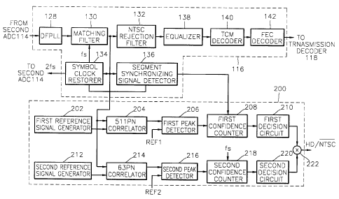
FIG. 2 is a detailed block diagram of the channel decoder 116 and the
15 discriminating circuit 200 shown in FIG. 1. In FIG. 2, a digital frequency
phase
locked loop (DFPLL) circuit 128 of the channel decoder 116 restores a carrier
wave using a pilot signal included in the data provided from the second ADC
114,
and demodulates the restored carrier wave into the baseband signal.
A matching filter 130 controls the symbol rate of the data provided from the
Zo DFPLL circuit 128 in order to remove signal distortion and aliasing from
the
demodulated baseband signal. Namely, the matching filter 130 controls the
symbol rate 2fs of the data provided from the DFPLL circuit 128 to be a symbol
clock fs.
An NTSC rejection filter 132 removes the component of the NTSC TV signal
25 included in the HDTV signal provided by the matching filter 130 since the
NTSC
TV signal operates as an interference when the NTSC TV signal coexists in the
HDTV channel.
A symbol clock restorer 134 restores the symbol clock in response to the
output of the matching filter 130 and the segment synchronizing signal
provided
so from the segment synchronizing signal detector 136 and applies a sampling
clock
having a frequency 2fs two times larger than that of the symbol clock to the
second ADC 114 shown in FIG. 1. The symbol clock fs restored by the symbol
clock restorer 134 is provided to other blocks for processing the digital
signal
4
CA 02256020 1998-12-14
though not shown in the drawings as well as the matching filter 130 and the
HD/NTSC discriminating circuit 200.
The segment synchronizing signal detector 136 detects the segment
synchronizing signal from the output of the matching filter 130. Namely, the
segment synchronizing signal detector 136 inputs the data controlled to have
the
symbol rate fs provided from the matching filter 130, obtains correlation
values in
units of four symbols, accumulates the obtained correlation values in units of
a
segment, and generates the segment synchronizing signal in a position in which
a
maximum accumulated correlation value is detected in every data segment since
the accumulated correlation value of each segment has the maximum value during
four segment synchronizing symbol sections.
An equalizer 138 updates and equalizes coefficients of a filter in the
equalizer using a known sequence inserted in the field synchronizing segment
in
order to remove a multipath distortion passing through the transmission
channel.
,s A Trellis-coded modulation (TCM) decoder 140 Trellis-decodes the output of
the
equalizer 138. A forward error correction (FEC) decoder 142 de-interleaves the
Trellis decoded data, Error-correction-decodes and de-randomizes the de-
interleaved data, and provides the data to the transmission decoder 118 shown
in
FIG. 1.
2o A first input port of a 511 pseudo number (PN) correlator 204 of the
HD/NTSC discriminating circuit 200 provided by the present invention is
connected
to the output port of the matching filter 130. A second input port thereof is
connected to the output port of a first reference signal generator 202. A
first input
port of a 63PN correlator 214 is connected to the output port of the matching
filter
2s 130. A second input port thereof is connected to a second reference signal
generator 212.
A first input port of a first peak detector 206 is connected to the output
port
of the 511 PN correlator 204. A first reference value REF1 is input to a
second
input port thereof. A first input port of a second peak detector 216 is
connected to
so the output port of the 63PN correlator 214. A second reference value REF2
is
input to a second input port thereof. An enable port of a first confidence
counter
208 is connected to the output port of the first peak detector 206. A clock
port
thereof is connected to the output port of the segment synchronizing signal
CA 02256020 1998-12-14
detector 136. An output port thereof is connected to a first decision circuit
210.
An enable port of a second confidence counter 218 is connected to the output
port
of the second peak detector 216. A clock port thereof is connected to the
output
port of the symbol clock restorer 134. An output port thereof is connected to
the
s output port of a second decision circuit 220. A discrimination signal
generator 222
can be comprised of a multiplier or an AND gate. First and second input ports
thereof are respectively connected to the output ports of the first and second
decision circuits 210. An output port thereof is connected to each control
port of
the display processor 122 and the DAC/mixer 124.
The operation of the HD/NTSC discriminating circuit 200 will be described
with reference to FIGs. 3 and 4. In FIG. 3, the HDTV signal provided from the
matching filter 130, i.e., the VSB data is input to each first input port of
the 511 PN
correlator 204 and the 63PN correlator 214.
Here, a VSB data frame is comprised of two fields as shown in FIG. 3.
,5 Each field is comprised of one field synchronizing segment and 312 data
segments. Each data segment is comprised of the segment synchronizing signal
of four symbols and 828 data symbols. The segment synchronizing signal is
inserted into a digital data stream having 8 levels in the front of the field
synchronizing segment and each data segment. The segment synchronizing
2o signal has a uniform pattern in which four symbols have a signal level of
"+5, -5, -
5, and +5". The remaining data of the data segment are randomly comprised of
an arbitrary signal level among eight levels (t1, t3, t5, and t7).
Field synchronizing signal sequences FIELD SYNC #1 and FIELD SYNC #2
showing the beginning of fields are inserted into field synchronizing segments
2s which are the first segments of the respective fields. Namely, as shown in
FIG. 4,
the field synchronizing segment is comprised of 832 symbols. The segment
synchronizing signal is positioned in the first four symbols. A 511 pseudo
number
(511 PN) is positioned in the next 511 symbols. Three 63PNs are positioned in
the
next 189 symbols. The additional information is existed to the remaining 128
so symbols. Here, since the 511 PN is a predetermined signal sequence
represented
by the +5 and -5 level, it is used in a signal processing block using a known
sequence such as equalization. In the second 63PN among the three 63PN,
phases are inverted alternately in every field. The field synchronizing signal
6
CA 02256020 1998-12-14
sequence showing the beginning of the field having the format shown in FIG. 4
is
inserted into the first segment of every field. The field synchronizing signal
sequence always has a uniform pattern.
The first reference signal generator 202 generates a pseudo random
s number in which the length of a reference signal is 511 (a 511 PN reference
signal). Namely, the first reference signal generator 202 locally and
repeatedly
generates the same signal as the 511 PN included in the field synchronizing
signal
sequence shown in FIG. 3. The second reference signal generator 212 generates
a pseudo random number in which the length of a reference signal is 63 (a 63PN
~o reference signal). Namely, the second reference signal generator locally
and
repeatedly generates the same signal as the 63PN included in the field
synchronizing signal sequence. In the present invention, the first reference
signal
generator 202 and the second reference signal generator 212 are separately
constructed in order to facilitate description. However, the 511 PN reference
signal
and the 63PN reference signal may be generated from single reference signal
generator.
The 511 PN reference signal and the 63PN reference signal generated from
the first reference signal generator 202 and the second reference signal
generator
212 are respectively provided to the second input ports of the 511 PN
correlator
20 204 and the 63PN correlator 214. Therefore, the 511 PN correlator 204
obtains
the correlation value of the 511 PN by accumulating the correlation values of
between the VSB data and the 511 PN reference signal in units of the 511
symbol.
The first peak detector 206 detects whether the correlation value of the 511
PN
provided from the 511 PN correlator 204 is no less than the first reference
value
25 REF1 and provides the first peak signal. The first peak signal is detected
in each
field.
The 63PN correlator 212 obtains the correlation value of the 63PN by
accumulating the correlation values of between the VSB data and the 63PN
reference signal in units of 63 symbol. The second peak detector 216 detects
3o whether the correlation value of the 63PN provided from the 63PN correlator
212
is no less than the second reference value REF2 and provides the second peak
signal. The second peak signal is alternately detected in every field two or
three
7
CA 02256020 1998-12-14
times. This is because phases are inverted alternately in every field in the
second
63PN among the three 63PNs.
At this time, the peak value is shown where the 511 PN signal and the 63PN
signal included in the field synchronizing signal sequence are positioned and
a
s value of almost "0" in places other than the field synchronizing signal
sequence.
Here, in order to simplify hardware, the 511 PN correlator 202 and the 63PN
correlator 212 can respectively detect the correlation value of the 63PN and
the
correlation value of the 511 PN by comparing only the sign bit of the input
VSB
data with the 63 PN reference signal and the 511 PN reference signal,
~o respectively.
The first confidence counter 208 verifies the confidence of the peak value
detected by the first peak detector 206 using the segment synchronizing signal
provided by the segment synchronizing signal detector 136. In the case of the
HDTV signal, the first peak signal is provided by the first peak detector 206
whenever the segment synchronizing signal is generated 313 times. Therefore,
the first confidence counter 208 receives the first peak signal as an enable
signal
when the first peak signal is detected by the first peak detector 206 and
counts the
segment synchronizing signal generated by the segment synchronizing signal
detector 136. The first confidence counter 208 counts the 313 segment
zo synchronizing signals and provides a logic "high" signal to the first
decision circuit
210 when the first peak signal is provided from the first peak detector 206.
The second confidence counter 218 verifies the confidence of the peak
value detected by the second peak detector 216. In the case of the HDTV
signal,
as shown in FIG. 4, the two second peak signals with respect to the first and
third
25 63PNs among the continuous three 63PNs are provided by the second peak
detector 216 in every field. Therefore, the second confidence counter 218
receives the beginning second peak signal of the second peak detector 216 as
an
enable signal, counts 126 symbol clocks generated by the symbol clock restorer
134, and provides the logic "high" signal to the second decision circuit 220
when
so the next second peak signal is input. Here, a distance between the first
symbol of
the first 63PN to the first symbol of the third 63PN is 126 symbols.
The first and second decision circuits 210 and 220 determine the logic
"high" signals continuously provided a predetermined number of times by the
first
8
CA 02256020 1998-12-14
and second confidence counters 208 and 218 to be the HDTV signals and provide
the first and second decision signals of the logic "high". Namely, the first
and
second decision circuits 210 and 220 observe the output signals of the first
and
second confidence counters 208 and 218 for a certain time, determine whether
periodicity exists, and determine whether the output signals are the HDTV
signals
or the NTSC TV signals. In the case of the HDTV signal, there is continuous
periodicity.
The multiplier of the discriminating signal generator 222 multiplies the
output of the first decision circuit 210 by the output of the second decision
circuit
220 and provides the discrimination signal HDlNTSC. Namely, the discrimination
signal generator 222 provides a discrimination signal of logic "high" showing
that
the output signals are the HDTV signals when periodicity is detected
simultaneously in both the first and second decision circuits 210 and 220.
When
there is no periodicity is in either of the two circuits 210 and 220, a
discrimination
~s signal of logic "low" showing that the output signals are~the NTSC TV
signal is
provided.
In FIG. 2, two channels exist for the confidence of the discrimination
circuit.
However, one channel may exist. Also, the present invention can be applied to
a
receiver for receiving a digital terrestrial wave HDTV signal to be broadcast
as well
Zo as the simulcast receiver which can simultaneously receive the NTSC TV
signal
and the HDTV signal. Namely, in the HDTV receiver, the channel selected by a
user indicating whether the selected channel is a HDTV channel or a NTSC
channel is displayed by a caption information according to the HD/NTSC
discrimination signal. In the present invention, the NTSC TV signal and the
HDTV
2s signal of a VSB modulation method are respectively described as an example
of
the signal of the analog broadcasting method and an example of the high
definition signal. A standard definition (SD) signal can be included in the
high
definition signal.
As mentioned above, according to the present invention, it is possible to
3o prevent mis-operation of the receiver since the received signal according
to
channel selection is the high definition signal or the signal of the analog
broadcast
method, thus meeting the needs of consumers.
9