Note: Descriptions are shown in the official language in which they were submitted.
CA 022~6~8~ l998- l2- l8
STRUCTURE FOR CONNECTING OPTICAL FIBERS TO OPTICAL WAVEGUIDE
BACKGROUND OF THE INVENTION
1. Field of the Invention
The present invention relates to a structure in which an optical fiber and an
5 optical waveguide are connected to each other, and more particularly, to an optical
fiber and optical waveguide connection structure in which optical fibers and an
optical waveguide are passively connected to each other on an arrangement
plafform.
2. Description of the Related Art
In general, an optical fiber array block module comprised of an array of
optical fibers, as many as the number of inpuVoutput waveguides of an optical
waveguide device, is fabricated to combine the optical waveguide device with theoptical fibers. The optical fiber array block module is formed by mounting an
optical fiber on a block having V-shaped grooves of uniform intervals, coating an
15 adhesive on the optical fiber, fixing the optical fiber with a coverlet, and polishing
the cross-section of the block. The inpuVoutput cross-section of the optical
waveguide device undergoes a polishing process to reduce a junction loss
occurring when coupled to the optical fiber array block module. After light is
waveguided to an input optical fiber of the optical fiber array block module, the
20 optical waveguides are accurately arranged such that a maximum output beam
can be emitted from the output end of the waveguide. While the maximum output
beam is emitted from the waveguide output end, the optical fiber array block
module and the optical waveguide device are fixed and finally coupled.
FIG. 1 shows a conventional optical waveguide device and a conventional
25 optical fiber array block module. Here, the arrangement of optical waveguide
devices 100 and an optical fiber array block module 110 is shown in a state justbefore being combined with one another. Three-dimensional coordinates on the
lower part of FIG. 1 are illustrated to show the direction of a beam to be irradiated
via the input end of the optical fiber array block module 110 and the arrangement
30 direction of each module. When the beam irradiated via the input end slips out of
CA 022~6~8~ l998- l2- l8
the output end of the optical fiber array block module 110 via the optical
waveguide device 100, an arrangement position with a minimum loss is found, to
thus complete the combination.
As described above, when the optical fiber array block module 110 and the
5 optical waveguide device 100 are combined in an active arrangement manner, an
optical source for emitting light is required, and a device such as an optical
detector for loss calculation must be included. Also, it takes much time and effort
to adjust the direction of arrangement.
SUMMARY OF THE INVENTION
To solve the above problems, it is an object of the present invention to
provide an optical fiber and optical waveguide connection structure in which an
optical waveguide device and an optical fiber array block are combined in a
passive arrangement manner so that they can be rapidly connected to each other
without a separate optical source.
Accordingly, to achieve the above object, there is provided an optical fiber
and waveguide connection structure comprising: optical fibers; an optical
waveguide device whose plane including a waveguide core stands out over the
surface of a substrate; and an arrangement platform which is placed so that the
center of each of the optical fibers can face the center of the waveguide core of
the optical waveguide device, and has depressed grooves for the optical fibers
and a depressed groove for the prominent portion of the optical waveguide device.
Preferably, when the optical waveguide device is mounted on the
arrangement plafform, a non-prominent substrate portion serves as a coverlet of
the optical fibers to be mounted on the arrangement platform.
It is preferable that the arrangement platform further comprises a supporter
for supporting an optical fiber portion extending from the depressed grooves when
the optical fibers are mounted on the depressed grooves.
It is preferable that on the arrangement platform, the height from the
surface of the groove etched to a depth where the prominent portion of the
waveguide device can fit to the center of the waveguide core when the waveguide
device is put into the depressed groove is the same as the radius of the cross-
section of each of the optical fibers.
CA 022~6~8~ l998- l2- l8
It is preferable that in the optical waveguide device, the height from the
substrate to the center of the optical waveguide device is the same as the radius
of the optical fiber cross-section.
To achieve the above object, there is provided an optical fiber and
waveguide connection structure comprising: optical fibers; an optical waveguide
device whose plane including a waveguide stands out over the surface of a
substrate; and an arrangement platform which is placed so that the center of each
of the optical fibers can face the center of the waveguide core of the optical
waveguide device, has V-caved grooves for the optical fibers and a depressed
groove for the prominent plane of the optical waveguide device, and includes a
supporter for supporting an extending portion of each of the optical fibers when the
optical fibers are mounted on the V-shaped grooves.
BRIEF DESCRIPTION OF THE DRAWINGS
The above object and advantages of the present invention will become
more apparent by describing in detail preferred embodiments thereof with
reference to the attached drawings in which:
FIG. 1 is a perspective view of a conventional optical waveguide device and
a conventional optical fiber array block module;
FIG. 2 is a perspective view of an optical fiber and optical waveguide
connection structure according to an embodiment of the present invention;
FIG. 3 is a perspective view of an optical fiber and optical waveguide
connection structure according to another embodiment of the present invention;
and
FIG. 4 is a perspective view of an optical fiber and optical waveguide
connection structure according to still another embodiment of the present
invention.
DESCRIPTION OF THE PREFERRED EMBODIMENTS
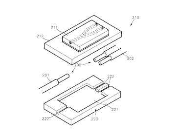
Referring to FIG 2, an optical fiber and optical waveguide connection
structure includes optical fibers 200, an optical waveguide device 210, and an
arrangement plafform 220. FIG. 2 shows an optical fiber 201 to be connected to
the input portion of the optical waveguide device 210 and optical fibers 202
CA 022~6~8~ l998- l2- l8
installed at a portion to which a signal passed through the optical waveguide
device 210 is output. The number of optical fibers 202 at the output portion
depends on the number of branches of the optical waveguide device 210. The
optical waveguide device 210 is etched until a prominent portion 211 including the
5 core of an optical waveguide stands out over the surface of a substrate 212. The
arrangement platform 220, on which the optical fibers 200 and the optical
waveguide device 210 are arranged and connected, has depressed grooves 222
for arranging the optical fibers 200 and a depressed groove 221 for housing the
prominent portion 211 of the optical waveguide device 210, formed on a substrate10 having a predetermined thickness. The depth of the depressed grooves for
arranging the optical fibers 200 must be equal to or a little smaller than the
diameter of the cross-section of the optical fibers. The depth of the depressed
groove 221 into which the prominent portion 211 of the optical waveguide device
210 is to be put is the same as those of the depressed grooves for the optical
fibers 200. When the optical fibers 200 and the optical waveguide device 210 arearranged and connected to each other on the arrangement plafform 220, the
center of each optical fiber, i.e., the center of the core of each optical fiber must
accurately contact the center of the optical waveguide device 210, i.e., the center
of the optical waveguide core. Such a connection must be properly calculated in
advance upon etching the depression of the arrangement plafform, to thus
accomplish accurate etching. The substrate 212 of the optical waveguide device
210 serves as a coverlet for fixing the optical fibers 200 to the optical waveguide
device 210 on the arrangement platform 220.
When the optical fibers 200 and the optical waveguide device 210 are
mounted and connected to each other on the arrangement plafform, the optical
fibers 200 is fixed by the substrate 212 of the optical waveguide device 210, i.e., a
substrate portion 212 which is not etched from the optical waveguide device 210.The prominent portion 211 of the optical waveguide device 210 is inserted into the
depression 221 of the arrangement plafform 220. Here, the height from the
substrate 212 of the optical waveguide device 210 to the center of the waveguidecore must be equal to the radius of the cross-section of the optical fibers 200.FIG. 3 shows an optical fiber and optical waveguide device connection
structure according to another embodiment of the present invention, comprising
CA 022~6~8~ l998- l2- l8
optical fibers 300, an optical waveguide device 310, and an arrangement platform320. The optical fibers 300 and the optical waveguide device 310 are the same
as described in FIG. 2. In the arrangement plafform 320, an arrangement part 322for connecting the optical fibers 300 to the optical waveguide device 310 exists on
5 a plate 321 for supporting the optical fibers, in contrast to FIG. 2. The depth of
the depression of the arrangement part 322 is the same as described in FIG. 2.
FIG. 4 shows an optical fiber and optical waveguide device connection
structure according to still another embodiment of the present invention,
comprising optical fibers 400, an optical waveguide device 410, and an
arrangement platform 420. The optical fiber 400 and the optical waveguide device410 are the same as described in FIG. 2. The arrangement plafform 420 is
comprised of a plate 421 for supporting the optical fibers 400 and an arrangement
part 422. The arrangement part 422 has a V-etched groove (V groove) for
mounting the optical fibers 400 and a depression into which the prominent portion
15 of the optical waveguide device 410 is to be fit. The etching depths of the Vgrooves 423 and the depressed groove 424 for the optical waveguide must be
smaller than or equal to the diameter of the cross-section of each of the optical
fibers 400. The height of the prominence 411 of the optical waveguide device 410must be controlled so that the height from the surface of a substrate 412 to the20 center of the waveguide core can be the same as the radius of the cross-section
of the optical fibers 400. The total height of the prominence 411 of the opticalwaveguide device 410 must be a little smaller than the diameter of the cross-
section of the optical fibers 400.
The characteristics and fabrication method of components for realizing
25 FIGS. 2 through 4 will now be described. A connection of the optical fibers to the
optical waveguide device depending on the combination of the components will be
described as follows. First, the arrangement platform 220, as a basic block in
which the optical fibers 200 and the optical waveguide device 210 are arranged, is
characterized in that it has a groove 221 for mounting the optical waveguide
30 device and grooves 222 for mounting optical fibers at an input and output portion
at predetermined intervals. Anisotropic etching of a silicon substrate can be used
to fabricate the arrangement platform 220. The arrangement plafform 220 of FIG.
2 is manufactured by forming an etch mask pattern of Si3N4, or other material on a
CA 022~6~8~ l998- l2- l8
silicon wafer excluding portions on which a waveguide device chip and an opticalfiber are to be mounted, and etching the pattern using an etch solution of KOH or
other solution. The arrangement plafform 420 of FIG. 4 is the case of
manufacturing the silicon wafer using the anisotropic etch method. The optical
waveguide devices 210, 310 and 410 of FIGS. 2 through 4 have the edge
removed to a predetermined depth so as to be accurately seated, respectively, onthe arrangement platforms 220, 320 and 420. Such an optical waveguide device
is realized by etching the edge of the optical waveguide device using a dry-etchmethod such as reactive ion etching (RIE) or by cutting the edge to a
predetermined depth using an accurate grinder. Here, the cross-section of an
input and output optical waveguide, i.e., the cross-section of an optical waveguide
to be connected to optical fibers at an input and output portion, must be accurately
processed to minimize optical loss upon connecting the optical fiber to the optical
waveguide. Here, the optical fiber also has an accurately-cut cross-section to
minimize optical loss when coupled to the cross-section of the input and output
optical waveguide.
The coupling between the components of FIGS. 2 through 4 will now be
described. In FIGS. 2 through 4, when the optical fiber, the optical waveguide
device, and the arrangement platform are coupled to one another, the optical
fibers are inserted into the grooves for mounting the optical fibers on the
arrangement plafform, and the optical waveguide device is put into the groove for
the optical waveguide device on the arrangement plafform, thereby completing thecoupling. Here, the cross-sections of the optical fibers and optical waveguide
meet and correspond to each other, and particularly, the optical fibers and the
optical waveguide core meet so as to have the same center. When the optical
fibers are mounted on the grooves of the arrangement plafform, about 20 to 30,umof the optical fibers protrudes from the surface extending from the grooves for
mounting the optical fibers on the arrangement plafform. When the optical
waveguide device is mounted on the arrangement plafform, a removed portion
(e.g., a portion of the substrate 212 of FIG. 2) of the edge of the optical
waveguide device serves as a plate for fixing the optical fibers. The diameter of a
typical optical fiber is 125~m, so the depth of the groove for mounting an optical
fiber on the arrangement plafform is about 95 to 105,um. In this way, the substrate
CA 022~6~8~ l998- l2- l8
portion being the etched-out edge of the optical waveguide device is mounted on
the optical fibers on the arrangement plafform upon coupling. When the radius ofeach of the optical fibers is 62.5,um, the center of the waveguide device core must
be 62.5,um high from the substrate surface of the optical waveguide device, i.e.,
5 from where the prominent portion begins to stand out, in order to match the center
of the core of the optical waveguide device with the center of the optical fiber.
Therefore, the optical fibers and the optical waveguide device are arranged
upward and downward, i.e., in the direction where an optical signal travels, on the
arrangement platform. The left-to-right length of the prominence-shaped plate of10 the optical waveguide device based on the input and output portion of the optical
waveguide core must be equal to the left-to-right length of the depression groove
of the arrangement platform, i.e., the length of a direction perpendicular to the
direction in which an optical signal travels. Also, the optical waveguide devicemust be manufactured in advance so that the center of its input and output portion
15 core can face the input and output portion of each of the optical fibers, thereby
allowing arrangement of the optical fibers and optical waveguide device in rightand left directions. As shown in FIGS. 3 and 4, the arrangement plafform plate for
supporting the optical fibers prevents damage to the optical fiber due to removal of
an optical fiber coating layer, when the optical fibers are mounted on the grooves
20 on the arrangement plafform. The aforementioned connection structure between
optical fibers and an waveguide device is achieved using a passive arrangement
method instead of an active arrangement method of attaching optical fibers to anoptical waveguide device, and thus does not require an optical source, an optical
detector, an accurate arrangement device, etc., which are necessary for active
25 arrangement connection.
According to the present invention, an optical source, an optical detector,
etc. are not used to connect the optical fiber to the optical waveguide based on a
passive arrangement structure, thus reducing the costs. Also, a rapid connectioncan be achieved.
, ~ .. . . , . ~ .,_ . , .