Note: Descriptions are shown in the official language in which they were submitted.
CA 022~6618 1998-ll-2~
WO 97/47059 PCT/US97l07549
InP-Based Lasers
with Reducecl Blue Shifts
FIELD OF THE INVENTION
The invention generally relates to semiconductor quantum-well structures. In
5 particular, the invention relates to InP and InGaAs quantum-well diode lasers whose
fabricational variations can be better controlled.
BACKGROUND ART
Many advanced electronic and opto-electronic integrated circuits are based on
compound semiconductors such as the III-V semiconductors. Gallium arsenide (GaAs) is the
10 basis of a fairly well developed technology, but indium phosphide (InP) and related materials
are not so well developed but have received much attention, especially for active opto-
electronic devices, such as lasers and optical modulators, operating in the 1.55~m band of
optical wavelengths which is of great interest for integration with silica optical fibers. Indium
gallium arsenide (InGaAs) is often considered to be an InP-based material because alloys with
15 InP can be made that have little change in lattice constant while providing bandgap control of
the commercially important part of the optical spectrum around 1550nm.
A fundamental advantage of III-V semiconductors is that modern film growth
techniques, such as organo-metallic chemical vapor deposition (OMCVD) and molecular
beam epitaxy (MBE), enable the epitaxial growth of thin films with nearly arbitrary III-V
20 compositions, assuming equality of Group-III cations and Group-V anions, thus allowing
many important semiconductor characteristics such as electronic bandgap to be freely
engineered. Similar freedom is available with II-VI semiconductors. An importantstructure that is so enabled is the single or multiple quantum-well (MQW) structure much
used for lasers and modulators, an example of which is illustrated schematically in FIG. 1
25 with the horizontal axis representing the epitaxial growth direction and the vertical axis
SUBSTITUTE SI~ET (RULE 26)
CA 022~6618 1998-11-2~
Wo 97/470s9 PCTIUSs7/07549
representing the electronic bandgap for the different materials. For example, an electronic
diode structure includes an n-type InP layer 10 and a p-type InP layer 12 sandwiching an
undoped active layer 14 comprising alternating thin layers of InGaAs wells 16 and InGaAsP
barriers 18. The wells and barriers 14 and 16 are thin enough, usually less than 10nm, that
5 one or more quantum mechanical valence states 20 and conduction states 22 form within
the wells 14. The number of quantum wells may be one or more.
The effective bandgap of the between the valence and conduction states 20, 22
within the wells 14 depend both upon the well composition and the thickness of the well.
Although the compositions are generally chosen to be lattice matched to the InP substrate, a
10 controlled amount of strain can be introduced into the wells and barriers to further control
the electronic band structure. The result is an active layer 14 having a high density of
narrow electronic states, assuming the wells 14 have been well fabricated, with the effective
bandgap that determines optical characteristics being easily varied. In a typical opto-
electronic device, electrical leads are connected to the two InP layers 10, 12 and an
15 unillustrated optical waveguiding structure is formed along the active layer 14 in the
directions perpendicular to the illustrated z-direction so as to confine a major portion of the
optical wave within the active layer 14 to there interact with the electrically controlled
carrlers.
However, the process of forming the optical confinement structure tends to the
20 degrade the multi quantum-well structure. A typical though simplified buried
heterostructure MQW laser is illustrated in cross section in FIG. 2. The vertical planar
structure of FIG. 1 is grown and then patterned and etched so as to form a ridge extending
along the y-direction and having a finite width along the x-direction of the active layer 14
including the multiple quantum wells. Thereafter, a semi-insulating InP 24 is epitaxially
25 regrown around the ridge to reduce the contrast of the refractive index of the active layer
14 relative to that of the surrounding material and to confine the biasing current to the
active layer 14. The structure shown in FIG. 2 is simplified for ease of presentation. More
layers may be included to, for example, better confine the light to the core, but the
illustrated structure is sufficient to explain the effect of the invention. More realistic
30 structures for buried heterostructure lasers are described by Odagawa et al. in "High-Speed
SUBSTITUTE SllE~ (RUL~ 26)
CA 022~6618 1998-ll-2~
Wo 97/47059 PCT/USg7/07549
Operation of Strained InGaAs/InGaAsP MQW Lasers Under Zero-Bias Condition," IEEEJournal of Quantum Electronics, vol. 29, 1993, pp. 1682-1686 and by Aoki et al. in
"Monolithic integration of DFB lasers and electroabsorption modulators using in-plane
quantum energy control of MQW structures, Inter~latio~1al Journal of High Speed
Electronics and Systems, vol. 5, 1994, pp. 67-90.
The regrowth of the fairly thick semi-insulating layer 24 imposes a large thermal
budget on the already fabricated quantum wells. Even the after grown upper cladding layer
12 incurs a significant thermal budget. OMCVD of these materials is typically done
between 625 and 650~C so that temperatures between 600 and 700~C should be anticipated.
Even higher temperatures may be required for explicit annealing. The thermal treatment of
the quantum wells in these temperature ranges has been generally observed to shift the
bandgap between the well states to the blue. That is, the effective bandgap of the well
states anneal to larger bandgap energy. Also, the potential wells tend to lose their
rectangular shape. The structure described by Aoki et al., ibid., includes both lasers and
modulators having different well thickness and involves two regrowths, one for the upper,
p-type InP layer and another for the semi-insulating InP. Thus significant blue shifting is
expected, but the amount of blue shift will differ between the laser and modulator because
of the differing well thicknesses.
The size of the blue shift has been observed to shift the photoluminescence peak by
about 10 ~o 40nm at devices designed for 1550nm. However, the shift varies across a wafer
and from wafer to wafer. A shift in the wavelength peak of the photoluminescent emission
presents a problem in fabricating lasers and modulators since, for example, optimum
performance in distributed feedback lasers requires the wavelength of the gain peak to
match the grating pitch. In the case of modulators, a variation of the blue shift between
different ones of the multiple quantum wells will produce a less steep change of absorption
with wavelength, thereby degrading the modulator performance.
Several suggestions have been made to reduce the blue shift. One entails the use of
substrates with high dislocation densities, the dislocation pipes acting as gettering sites for
~ the species, speculated to be phosphorus interstitials, responsible for the blue shift. This
SUBSTITUTE SHEET (RULE ~)
CA 022~6618 1998-ll-2~
WO 97147059 PCT/US97/07549
solution is not attractive because heavily dislocated substrates introduces concerns about
the reliability of devices formed on them.
Another suggestion involves the use of strained quantum wells in which both the
wells and the barriers have the same compositional ratio As/P of the Group-V components,
thereby avoiding any effect from the mobile phosphorus. Although this solution seems
effective, it restricts the device design.
Several groups have reported their understanding of the mechanism for blue shift in
Proceedings of Fifth International Conference on Indiunl Phosphide a~1d Related
Materials, April 19-22, 1993, Paris, France (IEEE Catalog #93CH3276-3). See Glew,
"Interdiffusion of InGaAs/InGaAsP quantum wells," ibid., pp. 29-32; Gillin et al., "Group V
interdiffusion in InO66GaO3lAs/InO66GaO3lAsO7POl quantum well structures," ibid., pp. 33-35;
Camassel et al., "l~xperimental investigation of the thermal stability of strained
InGaAs/InGaAsP MQWs," ibid., pp. 36-39; and Vettese et al., "An investigation into the
effects of thermal annealing on long wavelength InGaAs/InGaAsP multi-quantum well
lasers," Ibid., pp. 40-44. Although diffusion of phosphorus is a recurring theme, there is no
agreement on the responsible mechanism.
Accordingly, a more reliable and less restrictive method is desired for controlling
and reducing the blue shift in InP-based and related quaternary quantum-well structures.
SUMMARY OF THE INVENTION
The invention can be summarized as a quantum-well structure based on compound
semiconductors, particularly InP, InGaAs, and related III-V semiconductors, in which a
barrier layer is formed between the quantum wells and the substrate. Preferably, the barrier
layer contains aluminum, e.g., may be AlGaInAs, and it prevents the diffusion of species
from the substrate into the quantum wells that would otherwise cause a blue shift in the
quantum-well electronic states.
SUBSTITUTE S~IEET (RULE 26)
CA 022~6618 1998-ll-2~
WO 97/470sg PCTtUS97/07549
BRIEF DESCRIPTION OF THE DRAWINGS
FIG. l is a schematical representation of the composition and band structure of a
conventional semiconductor diode having a multi quantum-well active layer.
FIG. 2 is a cross-sectional view of a conventional buried heterostrllcture laser5 incorporating the multi quantum-well structure of FIG. 1.
FIG. 3 is a cross-sectional view of a first embodiment of the invention including an
AlGaInAs barrier layer below multiple InP-based quantum wells and above an InP buffer
layer.
FIG. 4 is a cross-sectional view of a second embodiment of the invention including
10 the AlGalnAs barrier layer below the InP buffer layer.
FIG. 5 is a cross-sectional view of a third embodiment of the invention including a
principal InP buffer layer and in which the AlGalnAs barrier layer is subdivided and
interleaved with additional InP buffer layers.
FIG. 6 is a cross-sectional view of a fourth embodiment of the invention which lacks
15 the principal InP buffer layer of the third embodiment.
FIG. 7 is cross-sectional view of a fifth embodiment of the invention including a
barrier layer formed over the quantum wells.
FIGS. 8 and 9 are cross-sectional view of sixth and seventh embodiments of the
invention is which the barrier layer is patterned to provide laterally varying blue shifts.
20 DETAILED DESCRIPTION OF T~IE PREFERRED EMBODIMENTS
According to the invention, a III-V semiconductor layer including a substantial
aluminum content acts as a diffusion barrier for quantum-well layers grown on its top. In a
particularly important application of the invention, a layer of AlGalnAs is epitaxially
deposited above an InP substrate to act as an effective diffusion barrier against species in
25 the substrate so as to protect quantum wells and barriers formed on the AlGaInAs barrier
layer. The quantum-well structure is composed of compound semiconductors, such as the
III-V material combinations of InGaAsP/InGaAs, InGaAsP/InGaAsP, InP/InGaAs, and
InP/InGaAsP.
SUBSTITUTE SHL~ET (RULE 26)
CA 022~6618 1998-ll-2~
WO 97/47059 PCT/US97/07549
The thickness of the barrier layer preferably lies within the range of 100nm to
500nm. The preferred AlGaInAs barrier material has a composition that is preferably lattice
matched to InP although it can be slightly strained as long as the thickness of a strained
layer does not exceed the pseudomorphic limit beyond which dislocations are generated.
5 Preferably, the AlGaInAs barrier material has an Al content between an AlInAs composition
and an AlGaInAs composition providing a bandgap wavelength of ~-1.3~m. The bandgap
energy of AIxGa~In~ x ~As that is lattice matched to InP is given by
E~,(eV) = 0.75 + 1.548x, (1)
with
l-x-~ = 0.53, (2)
and the bandgap wavelength is given by
~(nn1) = E ( V) (3)
10 The barrier layer may additionally contain other constituents to provide more complete
bandgap and strain engineering. In particular, some phosphorus may be included.
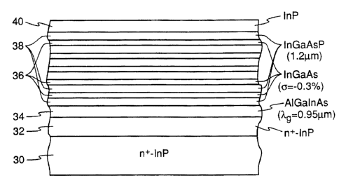
A first embodiment of the invention is shown in cross section in FIG. 3. On an
n+-type InP substrate 30 are epitaxially deposited an n~-type InP buffer layer 32 having a
thickness of 0.5 to 1.011m, over which is epitaxially deposited an AlGaInAs barrier layer 34
having a photoluminescent bandgap of ~L~=0.9511m. Its thickness is the range of 0.1 to
0.5,um. In general, in a diode structure the layers on opposite sides of the active region are
fairly heavily doped to opposite conductivity types. However, the doping is required only if
the layer is relatively thick. If their thickness is 0.1~m or less, undoped or partially doped
layers still provide the required conductivity to the active region. Here, an undoped 1~m-
20 thick AlGaInAs barrier layer 34 becomes part of the adjacent active region.
An undoped multi quantum-well structure is epitaxially deposited over the barrier
layer 34, and it includes 5 periods of alternating quantum-well layers 36 and barrier layers
38 plus an additional end barrier. The quantum-well layer 36 has a composition of
-6-
SUBSTITUTE SI~EET (F~U~E 26)
CA 022~6618 1998-ll-2~
WO 97/47059 PCT/US97/07549
InGaAs with a tensile strain of ~ = -0.3% and a thickness of 7nm. The barrier layer has a
composition of InGaAsP with ~=1.2~m and a thickness of 10nm. Over the quantum-well
~ structure is epitaxially grown an InP undoped protective capping layer 40 having a
thickness of about 0.1 ~m. The composition of the capping layer 40 was chose forexperimental purposes and to provide a close comparison to the comparative example. In
commercial devices, the capping layer may be formed of the quaternary InGaAsP although
it is not clear that would even be required. Other layers may be grown over the capping
layer 40 depending on the requirements of the optical structure. In any case, the AlGaInAs
barrier layer 34 prevents interdiffusion between the quantum-well structure 36, 38 and the
InP substrate 30. The specific structure, compositions, and thicknesses presented both
above and below are understood to be by way of example only. Alternative embodiments of
the invention may differ.
The second embodiment of the invention shown in the cross section of FIG. 4 differs
from that of FIG. 3 in that the AlGaInAs barrier layer 34 is placed beneath the InP buffer
layer 32 and the buffer layer 32 is adjacent to the quantum-well structure 36, 38. This
embodiment recognizes the fact that the l ,um-thick buffer layer 32 contributes little to the
diffusion of Group-V components, if indeed that is the cause of blue shifting, so that the
buffer layer 32 can be placed between the barrier layer 34 and the quantum-well structure
36, 38.
The third embodiment of the invention shown in the cross section of FIG. 5 differs
from the second embodiment of FIG. 4 in that the AlGaInAs barrier layer is divided into five
n+-type AlGaInAs (~g= 1.2~m) barrier sub-layers 44 interleaved with tour n+-type InP buffer
sub-layers 44 in a superlattice structure. The AlGaInAs barrier sub-layers 44 and the InP
buffer sub-layers 46 all have thicknesses, for example, of 0. l ~m. The buffer sub-layers 46
together with the initial InP buffer layer 32 present a high-quality substrate for subsequent
epitaxial growth while the barrier sub-layers 44 prevent interdiffusion of species within the
underlying InP into the quantum-well structure 36, 38. In the third embodiment, the
material immediately underlying the quantum-well structure 36, 38 is one of the barrier sub-
~ layers 44 so that not even a thin InP layer has unimpeded access to the quantum wells.
SUBSTITUTE S~ IFET (~ULE 2~)
CA 022~6618 1998-11-2~
WO 97/47059 PCT/US97/07549
The fourth embodiment of the invention illustrated in cross section in FIG. 6 differs
from the third embodiment of FIG. S in that it lacks the initial InP buffer layer 32, so that
the superlattice of the barrier and buffer sub-layers 44, 46 is grown directly on the substrate
30.
The fifth embodiment of the invention illustrated in cross section in FIG. 7 improves
upon the first embodiment of FIG. 3 in including a barrier layer above the quantum-well
structure. In particular, a thin upper InP protective layer 50 is epitaxially formed over the
quantum-well structure 36, 38 to a thickness of 10nm. This layer 50 was included for
experimental purposes and in commercial devices may be replaced by a quaternary InGaAsP
protective layer or dispensed with completely. Over the thin protective layer 50 are formed
an upper AlGaInAs barrier layer 52 having a thickness of 0.1~m and then the 0.1~1m-thick
InP capping layer 40. The upper barrier layer 52 protects the quantum-well structure 36, 38
from the phosphorus-containing phosphine environment used in an annealing step and also
protects it from interdiffusion from the InP capping layer 40 and whatever layers are formed
thereover, although it is not clear that interdiffusion from overgrown epitaxial layers is a
problem. In any case, the upper lnP protective layer 50 is so thin that it does not present a
signif1cant source of blue-shifting species.
In some of the experimental samples, up to 2,um of InP have been grown over an
quantum-well structure not protected on its upper side by a barrier layer. No blue shifts
have been attributed to this thick InP overlayer. It is thus believed that the species
responsible for blue shifts originates from the much thicker InP substrate.
Experiment
The inventive structure of the first embodiment of FIG. 3 was grown by OMCVD at
76Torr and at a growth rate of about 1.3nm/s. The precursor reagents were
trimethylgallium, trimethylalurninum, arsine, and phosphine in a carrier gas of hydrogen.
Hydrogen sulflde or disilane was used to obtain n-type doping; diethylzinc was used for
p-type doping. A comparative structure was grown with the same general structure and by
the same process, but it lacked the AlGaInAs barrier layer 34.
After the inventive and comparative structures were grown, they were both
subjected to a planar regrowth process typical of forming a buried MQW heterostructure
SUBSTITUTE SHEET (RULE 26)
CA 022~6618 1998-ll-2~
WO 97/47059 PCT/US97/07549
waveguide. Then, the quantum-well structure was tested for its photoluminescence, both
before and after the regrowth. The results are shown in TABLE 1.
Photoluminescence Blue Shift
Peak (nm)
Before Regrowth
(nm)
Inventive 1515 ~2
Example
Comparative1515 13.6-23.2
Example
TABLE 1
These data show that the blue shift of the 1515nm peak was reduced by almost a factor of
ten by use of the invention.
The invention allows the blue shift to be localized to selected areas of the opto-
electronic integrated circuit. Such a process is particularly useful for integrating both lasers
and modulators onto the same OEIC, the two elements requiring somewhat different peaks
in the MQW emission spectra. Similar selective blue shifting has been described by Francis
et al. in "Selective band-gap blueshifting of InGaAsP/InGaAs(P) quantum wells by thermal
15 intermixing with phosphorus pressure and dielectric capping," Journal of Applied Physic.s
vol. 75, 1994, pp. 3507-3510 and by Hamoudi et al. in "Controlled disordering ofcompressively strained InGaAsP multiple quantum well under SiO:P encapsulant andapplication to laser-modulator integration," Journal of Applied Physics, vol. 78, 1995,
pp. 5638-5641. The selective blue shifting of the invention provides more flexibility than
20 the process that described by Aoki et al., ibid., in achieving different characteristic
wavelengths in integrated lasers and modulators.
According to the invention, the selective localization of the blue shift is
accomplished by patterning one or more barrier layers. A sixth embodiment of theinvention utilizing localized blue shifting, illustrated in cross section in FIG. 8, differs from
25 the second embodiment of FIG. 4 in that a bottom AlGaInAs barrier layer 60 partially
SUBSTITUTE SH~I~ (RULE 26)
CA 022~6618 1998-ll-2~
WO 97/47059 PCT/US97/07549
underlying an InP buffer layer 62 beneath the quantum-well structure 36, 38 is patterned
into two sets of regions 64, 66. Except for the patterning, the barrier layer ~0 is same as
barrier layer 34 of FIG. 4 and the buffer layer 62 is the same as buffer layer 32 of FIG. 4,
but the buffer layer 62 additionally acts as a planarizing layer to smoothly cover the
apertured barrier layer 60. The first set of regions 64 include the barrier layer 60 and thus
experience minim~l blue shift; however, the barrier layer 60 does not does extend into the
second region 66, which thus experiences substantial blue shifting.
A related seventh embodiment of the invention patterns a barrier only above the
quantum wells. As illustrated in cross section in FIG. 9, the quantum-well structure 36, 38
is grown directly on the InP buffer layer 32 with no underlying barrier layer. Instead a
barrier layer 68 having the physical characteristics of the barrier layer 34 of FIGS. 3 and 4 is
deposited and patterned so that the barrier layer 68 exists in first regions 70 but is absent in
a second region 72. An InP capping layer 74 is deposited over the patterned barrier layer to
both protect the underlying structure and to planarize its upper surface.
In the seventh embodiment, the barrier layer 68 in the first regions 70 prevent the
further upward migration of the species responsible for the blue shift, which are relatively
free to migrate upwardly from the InP substrate 30. Hence, the species accumulates in the
quantum-well structure 36, 38 within the first regions 70 and a large blue shift is observed
there. However, in the second region 72 unprotected by an upper barrier, the blue shifting
species migrate through the quantum-well structure 36, 38 and continue upwardly from
there. Hence, some of the blue shifting species remains in the second region 72 but to a
lesser amount than in the first regions 74. Therefore, there is some blue shift in the second
region 72 but less than the blue shift in the first regions 70.
Although the patterned cross sections of FIGS. 8 and 9 show a fairly narrow
aperture in the t~arrier, a particularly useful application of the patterned blue shifting using
fairly large patterning and includes a MQW diode laser positioned within the lower-energy,
less blue-shifted region and an MQW optical modulator positioned within the higher-
energy, more blue-shifted region.
Although the examples and described embodiments of the invention have included
multiple quantum-wells, the invention can be applied to structures with single quantum
SUESTITUTE S~ )T (F~U! E 26)
CA 022~66l8 l998-ll-2~
Wo 97/47059 PCT/US97/07549
wells and other devices requiring very thin semiconductor layers where the thickness is
critical.
Although the quantum wells of the described embodiments have been incorporated
into a buried heterostructure laser waveguide, the invention is not so limited. Optical MQW
5 structures can be formed in a number of configurations and for different uses, for example,
the described optical modulators. Indeed, quantum wells can be advantageously used in
non-optical eleclrical circuits.
The invention thus provides an easy and economical method of reducing the blue
shift in quantum-well devices. For unpatterned barriers, an extra deposition step is required
l0 for each barrier layer or sub-layer, but the extra growth incurs little penalty. For patterned
barriers, an extra step of lithographically defining the barrier layer is required, but two
regions of differing bandgap are thereby obtained.
-
SUeST1TUTE S~I~ET (RULE 26)