Note: Descriptions are shown in the official language in which they were submitted.
CA 02256746 2003-O1-15
, 77496-11
ANTENNA MULLTIPLEXER WITH ISOLATION
OF SWITCHING ELEMENTS
FIE7~D OF THE INVENTION
This invention is related to circuitry for
mutiplexing a transmitter signal among a plurality of
antennas, and more particularly to an application of such
circuitry in an electronic article surveillance and
identification system.
BACKGROUND OF THE INVENTION
Copending U.S. Patent 5661457 dated August 26,
1997, which has a common inventor and a common assignee with
the present application, discloses an asset tracking and
control system that is operated to detect, in real time, the
whereabouts within a building of individuals or articles
which carry transponder devices. Tracking of individuals or
articles, by means of attached transponders, is carried out
by antenna configurations installed at selected portals
throughout the building. A preferred antenna configuration
disclosed in the '457 patent includes four antennas,
operated in time-division multiplexed fashion from a single
transmitter.
A known antenna multiplexing arrangement suitable
for application in the above-referenced asset tracking
system is indicated generally by reference numeral 10 in
Fig. 1. The arrangement 10 includes a transmit circuit 12
and antennas 14-1 and 14-2, interconnected by switching
circuitry 16. The switching circuitry 16 includes a switch
18-1 positioned for selectively open-circuiting an LC loop
1
CA 02256746 2003-O1-15
, 77496-11
formed by the transmit circuit 12 and the antenna 14-1, and
a switch 18-2 for open-circuiting a respective LC loop
formed by antenna 14-2 and the transmit circuit 12. (It is
to be understood that Fig. 1 is a simplified diagram,
omitting two of the four antennas that are normally driven
by one transmitter).
For the purposes of the asset identification,
1a
CA 02256746 1998-12-O1
~CT/us 9 7 i 0 9'1'? 9
~p~ 2 4 A P R 1998
tracking and surveillance system of the referenced '946
patent application, high speed switching is required, so
that the switches 18-1 and 18-2 are implemented using
MOSFETs or other transistor switches, rather than
mechanical relays. This known switching arrangement
suffers from a number of disadvantages. For example, the
MOSFET switches have considerable on resistances, and
produce substantial heat which can reduce the operating
life of the equipment. Also, there are significant
limitations on the maximum distance by which the antennas
14-1 and 14-2 may be separated from the transmit circuit
12. Even if expensive wiring using litz wire is used, the
maximum separation is about 25 feet. Although additional
transistor switches, indicated in phantom at 18'-1 and
18'-2, can be provided in parallel to reduce the on
resistance, this approach increases the cost of the
equipment and introduces added switch leakage which makes
it difficult to completely turn off the antennas.
2 0 OHJECTB 1111D 8010dARY OB T88 I~IVB~1TION
It is an object of the invention to provide an
antenna multiplexing arrangement for an article
surveillance system which operates with greater efficiency
than existing multiplexes arrangements.
It is a further object of the invention to provide an
antenna multiplexes arrangement in which switching losses
ass reduced.
It is still a further object of the invention to
provide an antenna multiplexes arrangement which
eliainates coupling between adjacent antennas.
According to a first aspect of the invention, there
is provided a transmitter for an electronic article
surveillance system, including transmit circuitry for
generating a transmit signal, antenna circuitry for
receiving the transmit signal generated by the transmit
circuitry and for radiating the transmit signal into an
interrogation zone as an interrogation signal, and
connecting circuitry for transmitting the transmit signal
2
~E~,ypEp 3HEE'(
CA 02256746 1998-12-O1
WO 97/49075 PCT/US97/09779
from the transmit circuitry to the antenna circuitry, the
connecting circuitry including first coupling circuitry
for coupling the connecting circuitry to the transmit
circuitry, and second coupling circuitry for coupling the
connecting circuitry to the antenna circuitry, the first
coupling circuitry having a f first impedance and the second
coupling circuitry having a second impedance that is
matched to the first impedance.
Further in accordance with this aspect of the
invention, the antenna circuitry may include a first
antenna and a second antenna, and the connecting circuitry
includes switching circuitry for selectively uncoupling at
least one of the first and second antennas from the
transmit circuitry. The first antenna may include a first
antenna coil for radiating the transmit signal in the
interrogation zone, the second antenna may include a
second antenna coil for radiating the transmit signal in
the interrogation zone, the second coupling circuitry of
the connecting circuitry includes a first winding
inductively coupled to the first antenna coil and a second
winding inductively coupled to the second antenna coil,
and the switch circuitry of the connecting circuitry
includes a f first switch connected across the f first winding
for selectively short-circuiting the first winding and a
second switch connected across the second winding for
selectively short-circuiting the second winding. Further,
the first coupling circuitry may be a transformer having
a primary winding and a secondary winding with the
secondary winding having the above-mentioned first
impedance. Furthermore, the second coupling circuitry may
include a first transformer for coupling the connecting
circuitry to the first antenna and a second transformer
for coupling the connecting circuitry to the second
antenna. In that case, the switch circuitry may include
a first switch connected across a winding of the first
transformer for selectively short-circuiting that winding
of the first transformer, and a second switch connected
across a winding of the second transformer for selectively
3
CA 02256746 1998-12-O1
WO 97/49075 . PCT/US97J09779
short-circuiting that winding of the second transformer.
Further, the antenna circuitry may include third and
fourth antennas in addition to the first and second
antennas previously mentioned.
According to another aspect of the invention, there
is provided apparatus for interconnecting a transmitter
and a plurality of antennas, the transmitter having first
and second terminals, the plurality of antennas having a
first antenna having a first antenna coil and a second
l0 antenna having a second antenna coil. The apparatus
includes a step-down transformer having a primary winding
connected across the first and second terminals of the
transmitter and a secondary winding, a first winding
positioned for inductively coupling with the first antenna
coil of the first antenna, a second winding positioned for
inductively coupling with the second antenna coil of the
second antenna, a first switch, wiring for forming a
series loop connection which includes the first winding,
the second winding, the first switch, and the secondary
winding of the transformer, where the first switch is
arranged to selectively open-circuit the series loop
connection, a second switch connected across the second
winding for selectively short-circuiting the second
winding, and a third switch connected across the first
winding for selectively short-circuiting the first
winding. The apparatus may also include a third antenna
having a third antenna coil, with a third winding
positioned for inductively coupling with the third antenna
coil of the third antenna, a fourth switch connected
across the third winding for selectively short-circuiting
the third winding, a fourth antenna having a fourth
antenna coil, a fourth winding positioned for inductively
coupling with the fourth antenna coil of the fourth
antenna, and a fifth switch connected across the fourth
winding for selectively short-circuiting the fourth
winding. The third and fourth windings are connected to
the secondary winding in a second series loop connection
that is in parallel with the above-mentioned series loop
4
CA 02256746 1998-12-O1
WO 97/49075 . PCT/US97/09779
connection, and a sixth switch is provided to selectively
open-circuit the second series loop connection.
According to a further aspect of the invention, there
is provided a method of selectively energizing one of a
plurality of antennas to radiate a signal generated by a
transmitter circuit, each of the plurality of antennas
having a respective antenna coil, and the method including
the steps of providing a plurality of windings connected
in series, each of the windings corresponding to, and
to inductively coupled with, a respective one of the antenna
coils, the series-connected windings being coupled to the
transmitter circuit, and short-circuiting all but one of
the windings to select for energizing the antenna coil
corresponding to the winding that is not short-circuited.
According to yet another aspect of the invention,
there is provided apparatus for interconnecting a
transmitter and a plurality of antennas, the transmitter
having first and second terminals, the plurality of
antennas including a first antenna having a first antenna
coil and a second antenna having a second antenna coil,
the apparatus including a first winding positioned for
inductively coupling with the first antenna coil of the
first antenna, a second winding positioned for inductively
coupling with the second antenna coil of the second
antenna, a first switch, wiring for forming a series
connection of the first winding, the second winding and
the first switch, circuitry for coupling to the
transmitter the series connection of the first winding,
the second winding and the first switch, a second switch
connected across the second winding for selectively short
circuiting the second winding, and a third switch
connected across the first winding for selectively short
. circuiting the first winding.
Further in accordance with the latter aspect of the
invention, the coupling circuitry may include a
transformer for stepping down a level of a signal output
from the transmitter to form a signal to be applied across
the series connection of the first winding, the second
5
CA 02256746 1998-12-O1
WO 97/49075 . PCT/US97/09779
winding and the first switch.
According to still a further aspect of the invention,
there is provided an antenna multiplexes for supplying a
radio frequency signal to a selected one of a plurality of
antennas, including a plurality of transistor switches,
for selecting respective ones of said plurality of
antennas and each having a gate terminal, circuitry for
filtering the radio frequency signal to form a bias
signal, and circuitry for selectively coupling the bias
signal to the respective gate terminals of the transistor
switches.
The plurality of transistor switches may include
stacked pairs of FETs, each pair of FETs corresponding to
a respective one of the antennas. The bias signal may be
selectively coupled to each pair of FETs for de-selecting
the antenna which corresponds to the respective pair of
FETs. The coupling circuitry may include a plurality of
opto-isolators, each for controlling coupling of the bias
signal to a respective one of the pairs of FETs.
The foregoing and other objects, features and
advantages of the invention will be further understood
from the following detailed description of preferred
embodiments and practices of the invention and from the
drawings, wherein like reference numerals identify like
components and parts throughout.
DESCRIPTION OF THE DRAWINGS
Fig. 1 is a block diagram of a conventional antenna
multiplexes arrangement.
Fig. 2 is a block diagram of an antenna multiplexes
arrangement provided in accordance with the invention.
Fig. 3 is another block diagram representation of the
multiplexes arrangement of Fig. 2, including a switching
module provided adjacent to a transmit circuit.
Fig. 4 is a block diagram of an antenna multiplexes
arrangement provided in accordance with a second
embodiment of the invention.
Fig. 5 is a block diagram of an antenna multiplexes
6
CA 02256746 1998-12-O1
WO 97/49075 , PCT/US97/09779
arrangement provided in accordance with a third embodiment
of the invention.
Fig. 6 is a block diagram of an antenna multiplexes
arrangement provided in accordance with a fourth
embodiment of the invention.
Fig. 6A is a block diagram of an antenna multiplexes
arrangement provided in accordance with a fifth embodiment
of the invention.
Fig. 7 is a schematic illustration of a conventional
switch control technique.
Fig. 8 is a schematic illustration of switch control
circuitry provided in accordance with the present
invention.
DESCRIPTION OF PREFERRED EMBODIMENTS AND PRACTICES
Antenna multiplexes circuitry provided in accordance
with a first embodiment of the invention will now be
described with reference to Fig. 2. The arrangement of
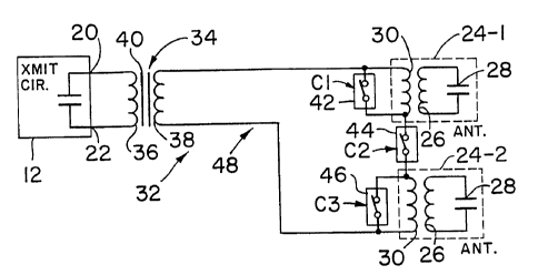
Fig. 2 includes a transmit circuit 12, which may be the
same as the conventional transmit circuit described in
connection with Fig. 1. The transmit circuit 12 includes
a first terminal 20 and a second terminal 22. The
transmit circuit 12 may be of the type used in the TIRIS
radio frequency identification system marketed by Texas
Instruments. In the TIRIS system, the transmit circuit
generates bursts at 134.2 kHz and the signal is
transmitted through antennas to energize transponders that
are attached to objects or individuals to be identified.
The arrangement of Fig. 2 includes antennas 24-1 and
24-2. Each of the antennas includes an antenna coil 26
and a capacitance 28 connected across the coil 26 to form
a resonant circuit with the coil 26. The antenna coil 26
is preferably formed as a planar, rectangular, air-core
coil formed of three turns.
Each of the antennas includes a coupling winding 30
arranged in proximity to the antenna coil 26 for inductive
coupling with the antenna coil 26. For example, the
coupling winding 30 may be formed as a single turn
7
CA 02256746 1998-12-O1
WO 97149075 . PCT/US97/09779
adjacent to, in the plane of , and around the periphery of ,
the planar-rectangular antenna coil 26.
The coupling windings 30 of the antennas 24-1 and 24
2 are connected to the terminals 20 and 22 of the transmit
circuit 12 by means of multiplexing and impedance-matching
circuitry 32. The circuitry 32 includes a step-down
transformer 34. The transformer 34 includes a primary
winding 36 connected between the terminals 20 and 22 of
the transmit circuit 12, and a secondary winding 38
inductively coupled to the primary winding 36 via a core
40.
Also included in the circuitry 32 are switches 42, 44
and 46. Wiring is provided to form a loop series
connection 48 interconnecting in series the secondary
winding 38 of the transformer 34, the respective coupling
windings 30 of the antennas 24-1 and 24-2 and the switch
44. The switch 44 operates so as to selectively open-
circuit the loop series connection 48. Although the
switch 44 is shown in Fig. 2 as being connected between
the respective coupling windings 30 of the antennas 24-1
and 24-2, the switch 44 may also be positioned at any
other point in the loop series connection 48.
Switch 42 is connected across the coupling winding 30
of the antenna 24-1 so that the winding 30 of antenna 24-1
can be selectively short-circuited, and thus effectively
removed from the loop connection 48. Similarly, switch 46
is connected across the winding 30 of the antenna 24-2 so
that the winding 30 of the antenna 24-2 can be selectively
short-circuited and thereby effectively removed from the
loop 48. Control signals C1, C2 and C3 are respectively
provided to the switches 42, 44 and 46 to switch the
switches 42, 44 and 46 between open and closed states.
The- control signals C1, C2 and C3 are provided by a
control circuit which is not shown.
The transformer 34 steps down the high voltage signal
provided at the terminals of the transmit circuit 12, and
the impedance of the secondary winding 38 of the
transformer 34 is matched to the respective impedances of
8
CA 02256746 1998-12-O1
PCT/US 9 7 / 0 9 ? 'l 9
~~~ 2 4 A P R 1998
the windings 30 of the antennas 24-1 and 24-2.
Consequently, current and voltage are in phase in the loop
connection 48, and the current and voltage levels are
relatively low in comparison with the high voltage and
high current signals in the tuned circuits at the transmit
circuit 12 and the antennas 24-1 and 24-2. The switches
42, 44 and 46 can therefore be implemented using
- relatively small, efficient and low cost solid state
switches, thereby providing cost savings and improved
l0 power efficiency in comparison with the conventional
multiplexing arrangement of Fig. 1.
When antenna 24-1 is to be selected for operation,
switch 42 is opened and switches 44 and 46 are closed. As
a result, the antenna coil 26 of antenna 24-1 is
effectively coupled to the transmitter 12 and radiates the
signal generated by the transmitter into the interrogation
zone as a signal which interrogates any transponder
present in the interrogation zone.
When antenna 24-2 is to be selected for operation,
switch 46 is opened and switches 42 and 44 are closed, and
the antenna coil 26 of antenna 24-2 is energized to
radiate the interrogation signal. When switch 44 is
opened, antennas 24-1 and 24-2 are both effectively
disconnected from the transmit circuit 12.
Providing a short-circuit across the respective
coupling winding 30 when an antenna is not selected for
operation, prevents coupling between adjacent antennas,
and crosstalk from the non-selected antenna.
Fig. 3 is another representation of the multiplexing
arrangement of Fig. 2. In Fig. 3, the switches 42, 44 and
46 shown in Fig. 2 are represented by a switching module
50 provided between the transformer 34 and the antennas
24-1 and 24-2. As indicated in Fig. 3, the switching
module 50 preferably is provided adjacent to the
transformer 34, which, in turn, ie preferably located
close to the transmit circuit 12. In this way, the signal
paths for the control signals C-1, C-2 and C-3 can be
relatively short, it being assumed that the control
9
~h~NDED S
CA 02256746 1998-12-O1
WO 97/49075 , PCT/US97/09779
circuit (which is not shown) for generating the control
signals is located in proximity to the transmit circuit
12. On the other hand, because the switches incorporated
in the switching module 50 are such as to provide rather
low losses, the antennas 24-1 and 24-2 may be located at
a considerable distance from the transmit circuit 12 and
its associated transformer 34, and relatively inexpensive
standard wiring can be used instead of the litz wire used
in conventional installations.
A second embodiment of the invention will now be
described with reference to Fig. 4. The arrangement of
Fig. 4 has the same transmit circuit 12, transformer 34
and antennas 24-1 and 24-2 as the arrangement of Fig. 2.
However, the multiplexing and impedance-matching circuitry
32' of Fig. 4 is different from the circuitry 32 of Fig.
2, in that, in the Fig. 4 arrangement, antennas are de-
selected by opening a switch provided in series with the
respective coupling winding 30, rather than closing a
switch connected across the coupling winding, as was done
in the arrangement of Fig. 2. Specifically, the
arrangement of Fig. 4 includes a switch 52 connected to
selectively open-circuit a first loop formed of the
secondary winding 38 of the transformer 34 and the
coupling winding 30 of the antenna 24-1, and a switch 54
provided to selectively open-circuit a second loop which
includes the secondary winding 38 and the respective
coupling winding 30 of the antenna 24-2.
It will be understood that, when an antenna is not
selected to transmit the interrogation signal, neither the
antenna coil nor the coupling winding is short-circuited
in the arrangement shown in Fig. 4. However, as is
suggested by the ellipses 56 in Fig. 4, the antennas 24-1
and 24-2 are assumed to be at a considerable distance from
each other, so that crosstalk and coupling between the two
antennas is not a concern.
A third embodiment of the invention is illustrated in
Fig. 5. The embodiment of Fig. 5 includes the same
transmit circuit 12, transformer 34 and switches 42, 44
CA 02256746 1998-12-O1
-PCT/tfS 9 7 / 0 9 7~7~9
IP'EA~US 2 4 APR 1998
and 46 as the embodiment of Fig. 2. However, in the
embodiment of Fig. 5, antennas 24'-1 and 24'-2 differ from
the antennas shown in Fig. 2, in that~the antennas of Fig.
do not include the coupling winding 30. Instead, the
5 antenna coils 26 are coupled to the transmit circuit 12
by
respective step-up transformers 58-1 and 58-2. Each of
the step-up transformers includes a primary winding 60,
a
secondary winding 62 and a core 64 which inductively
couples the windings of the step-up transformer. A series
loop connection 48' is formed in the arrangement of Fig.
5, with the primary windings 60 of the transformers 58-1
and 58-2 taking the place of the coupling windings 30
shown in Fig. 2. Each of the secondary windings 62 is
coupled to the antenna coil 26 of the respective antenna
24'-1 or 24'-2. The respective impedances of the primary
windings 60 match the impedance of the secondary winding
38 of the transformer 34.
As in the arrangement of Fig. 2, the switches 42, 44
and 46 are in a relatively low current, low voltage loop
and therefore may be smaller, more efficient, and less
costly than transistor switches used in conventional
antenna multiplexing arrangements. Also, as in the case
of the embodiment of Fig. 2, non-selected antennas are
effectively short-circuited (by the short-circuiting of
the primary 60 of the corresponding transformer 58-1 or
58-2) , so that crosstalk and coupling between the antennas
'~-- is prevented.
hig. 6 illustrates a fourth embodiment of the
invention. The embodiment of Fig. 6 is like that of Fig.
2, but with the addition of two more antennas (24-3 and
24-4), bringing the total number of antennas to four. It
will be noted that, in the embodiment of Fig. 6, all four
of the coupling windings 30 are in the same loop
connection (indicated by 48 " in Fig. 6), and that
additional antenna selection switches 66 and 68 are
provided, respectively connected across the coupling
windings 30 of the antennas 24-3 and 24-4. When one of
the antennas is selected to transmit the interrogation
11
AMENDED SHEET
CA 02256746 1998-12-O1
WO 97/49075 PCT/US97/09779
signal, the corresponding one of antenna selection
switches 42, 46, 66 and 68 is opened, while all of the
other antenna selection switches are closed, along with
the loop switch 44.
Fig. 6A illustrates a fifth embodiment of the
invention. As in the embodiment of Fig. 6, four antennas
are multiplexed, but two parallel loops, each for
interfacing to two antennas, are provided instead of a
single loop for interfacing to all four antennas.
Specifically, in the fifth embodiment wiring is provided
to form a loop series connection, indicated by reference
numeral 69, among secondary winding 38 of the transformer
34 and the coupling windings 30 which respectively
correspond to the antennas 24-3 and 24-4. A switch 67 is
provided to selectively open-circuit the loop connection
69. The loop connection 69 is in parallel with the loop
connection 48, which is the same as in the embodiment of
Fig. 2.
According to another aspect of the invention, an
advantageous technique for coupling control signals to the
antenna selection switches is provided. Before this
technique is described, a prior art control signal
coupling technique will be discussed with reference to
Fig. 7. According to the known control technique, three
stacked pairs of MOSFETs {Q1 and Q2; Q3 and Q4; Q5 and Q6)
are provided in parallel in the path to ground from the
antenna to be controlled by the parallel switches. As
indicated in the earlier discussion of Fig. 1, the
parallel switching pairs are provided to reduce the on
resistance. A gate biasing signal for the switching
transmitters is taken from the system 12-volt power supply
through MOSFET Q13 and associated resistors 70 and 72. An
opto-isolator 74 is driven by a switch control signal to
selectively short the gate biasing signal to the source
side of the switching transistors, thereby disabling the
switching transistors and de-selecting the antenna
controlled by the switching transistors.
In the switch control technique provided in
12
CA 02256746 1998-12-O1
WO 97/49075 . PCT/US97/09779
accordance with the present invention, the bias signal
applied to the gate terminals of the switching transistors
is derived from the RF signal to be supplied to the
antennas, and not from the system power supply. This
allows a reduction in component count, while permitting
complete isolation of the switching circuitry from the
balance of the system. This technique takes advantage of
the fact that a reduced number of switching transistors,
suitable for low current applications, is used in the
antenna multiplexing arrangements described in connection
with Figs. 2-6.
Details of this advantageous switch control practice
will now be described with reference to Fig. 8.
The circuitry shown in Fig. 8 includes dual RF buses
76 and 78 for transmitting the RF antenna driving signal
from the secondary winding 38 (Fig. 2). Continuing to
refer to Fig. 8, a stacked pair of MOSFETs Q8 and Q10
correspond to the switch 42 of Fig. 2, and a stacked pair
of MOSFETs Q11 and Q12 correspond to the switch 46 of Fig.
2. The loop switch 44 of Fig. 2 is represented by the
MOSFETs Q7 and Q9 in Fig. 8. Terminals E11 and E12 are
provided to connect the circuitry of Fig. 8 to the
coupling winding 30 of antenna 24-1 and terminals E13 and
E14 are provided to connect the circuitry of Fig. 8 to the
coupling winding 30 of antenna 24-2. The bias signal to
be selectively provided to the gate terminals of MOSFETs
Q8 and Q10 is derived from the RF signal on bus 78 by a
filter network made up of resistor R6, diode CR6, zener
CR13 and capacitor C6.
To select antenna 24-1 for transmission of the
interrogation signal, an antenna select signal
(corresponding to control signal C-1, Fig. 2, and provided
by control logic which is not shown) actuates opto-
isolator 80, which causes the filtered RF signal to be
shorted to the common source connection of the MOSFETs Q8
and Q10, thus disabling the MOSFETs and eliminating the
short-circuit connection which, when the MOSFETs are
operative, removes antenna 24-1 from effective connection
13
CA 02256746 1998-12-O1
WO 97/49075 . PCT/US97109779
to the transmitter. For the MOSFET pair Q11 and Q12,
which control connection to the antenna 24-2, a similar RF
signal filter network is provided, made up of resistor R5,
diode CRS, zener CR14 and capacitor C7. In similar manner
to the above-noted operation of the switches controlling
antenna 24-l, the MOSFETs 11 and 12 are selectively
disabled by application of a control signal C2 applied to
opto-isolator 82.
It will be observed that the signal selectively
supplied to the gate terminals of the MOSFETs Q7 and Q9 is
also derived from the RF signal, filtered through
resistors R7 and R8, diodes CR7 and CR8, zener CR9 and
capacitor C8. A combination of opto-isolators 84 and 86
provides for MOSFETs Q7 and Q9 to be conducting only when
one of the other MOSFET pairs is disabled.
By deriving the gate bias signals from the RF signal
to be supplied to the antennas, complete isolation of the
antennas and the associated switches is accomplished,
thereby reducing component count, and eliminating the need
to reference the antennas and the associated switches to
the transmit circuit power supply.
Although a switching arrangement for only two
antennas is shown in Fig. 8, it will be appreciated that
the four antenna embodiment of Fig. 6 can be implemented
in a similar manner.
In each of the embodiments described up to this
point, a step-down transformer 34 has been provided at the
transmitter side of the multiplexing circuit 32. However,
it is contemplated to replace the step-down transformer
with a suitable impedance-matching network.
Various other changes in the foregoing apparatus and
modifications in the described practices may be introduced
without departing from the invention. The particularly
preferred methods and apparatus are thus intended in an
illustrative and not limiting sense. The true spirit and
scope of the invention is set forth in the following
claims.
14