Language selection

Search

Patent 2257047 Summary

Third-party information liability

Some of the information on this Web page has been provided by external sources. The Government of Canada is not responsible for the accuracy, reliability or currency of the information supplied by external sources. Users wishing to rely upon this information should consult directly with the source of the information. Content provided by external sources is not subject to official languages, privacy and accessibility requirements.

Claims and Abstract availability

Any discrepancies in the text and image of the Claims and Abstract are due to differing posting times. Text of the Claims and Abstract are posted:

  • At the time the application is open to public inspection;
  • At the time of issue of the patent (grant).
(12) Patent: (11) CA 2257047
(54) English Title: AUTO AUDIO/VIDEO OUTPUT CIRCUIT WITH MULTIPLE AUDIO/VIDEO INPUTS
(54) French Title: CIRCUIT DE SORTIE AUDIO/VIDEO AUTOMATIQUE AVEC ENTREES AUDIO/VIDEO MULTIPLES
Status: Expired and beyond the Period of Reversal
Bibliographic Data
(51) International Patent Classification (IPC):
  • G11B 31/00 (2006.01)
  • H04N 05/44 (2011.01)
  • H04N 05/46 (2006.01)
  • H04N 05/775 (2006.01)
(72) Inventors :
  • HO, CHIN-CHI (Taiwan, Province of China)
(73) Owners :
  • JOIN COMPUTER CO., LTD.
(71) Applicants :
  • JOIN COMPUTER CO., LTD. (Taiwan, Province of China)
(74) Agent: SMART & BIGGAR LP
(74) Associate agent:
(45) Issued: 2002-08-27
(22) Filed Date: 1998-12-24
(41) Open to Public Inspection: 2000-06-24
Examination requested: 2001-02-08
Availability of licence: N/A
Dedicated to the Public: N/A
(25) Language of filing: English

Patent Cooperation Treaty (PCT): No

(30) Application Priority Data: None

Abstracts

English Abstract


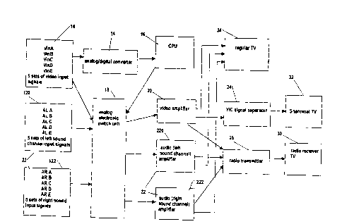
An auto audio/video output circuit with multiple audio/video
inputs, the circuit having an analog/digital converter unit for convert
inputted video signal into digital signal, a CPU for memorizing the
sequence of inputted audio/video signals, permitting the last
inputted audio/video signal to be outputted to audio/video output
amplifiers for amplification and further output to a TV.


Claims

Note: Claims are shown in the official language in which they were submitted.


What the invention claimed is:
1. An auto audio/video output circuit comprising:
a video input interface having a plurality of signal input
terminals for receiving video signal from at least one audio/video
equipment, and a plurality of signal output terminals;
at least one audio input interface each having a plurality of
signal input terminals for receiving audio signal from at least one
audio/video equipment and a plurality of signal output terminals;
at least one analog/digital converter respectively connected
to the signal output terminals of said video input interface for
converting video signal into corresponding digital signal;
a CPU (central processing unit) having a plurality of signal
input pins respectively connected to respective signal output
terminals of said at least one analog/digital converter for receiving
converted digital signals from said analog/digital converter,
permitting received digital signals to be memorized in proper order
in memory means in said CPU, and a control signal output pin;
an analog electronic switch unit having a plurality of signal
input terminals respectively connected to the signal output terminals
of said video input interface and the signal output terminals of said
at least one audio input interface, a plurality of signal output
terminals, and a control terminal connected to the control signal
8

output pin of said CPU to receive a control signal from said CPU for
controlling the closing/opening of the signal output terminals of said
electronic switch unit;
a video output amplifier having a plurality of video signal
input terminals respectively connected to the signal output terminals
of said analog electronic switch unit to receive video signals from
said analog electronic switch unit, and a video signal output terminal;
and
an audio output amplifier having a plurality of signal input
terminals respectively connected to the signal output terminals of
said analog electronic switch unit to receive audio signals from said
analog electronic switch unit and a plurality of audio signal output
terminals;
wherein the video signal output terminal of said video output
amplifier and the audio signal output terminals of said audio output
amplifier are respectively connected to the video input terminal and
audio input terminals of a TV for output.
2. An auto audio/video output circuit comprising:
a video input interface having a plurality of signal input
terminals for receiving video signal from at least one audio/video
equipment, and a plurality of signal output terminals;
at least one audio input interface each having a plurality of
9

signal input terminals for receiving audio signal from at least one
audio/video equipment and a plurality of signal output terminals;
at least one analog/digital converter respectively connected
to the signal output terminals of said video input interface for
converting video signal into corresponding digital signal;
a CPU (central processing unit) having a plurality of signal
input pins respectively connected to respective signal output
terminals of said at least on8 analog/digital converter for receiving
converted digital signals from said analog/digital converter,
permitting received digital signals to be memorized in proper order
in memory means in said CPU, and a control signal output pin;
an analog electronic switch unit having a plurality of signal
input terminals respectively connected to the signal output terminals
of said video input interface and the signal output terminals of said
at least one audio input interface, a plurality of signal output
terminals, and a control terminal connected to the control signal
output pin of said CPU to receive a control signal from said CPU for
controlling the closing/opening of the signal output terminals of said
electronic switch unit;
a video output amplifier having a plurality of video signal
input terminals respectively connected to the signal output terminals
of said analog electronic switch unit to receive video signals from
10

said analog electronic switch unit, and a video signal output terminal;
and
an audio output amplifier having a plurality of signal input
terminals respectively connected to the signal output terminals of
said analog electronic switch unit to receive audio signals from said
analog electronic switch unit and a plurality of audio signal output
terminals; and
a radio transmitter connected to the signal output terminals
of said analog electronic switch unit;
wherein the video signal output terminal of said video output
amplifier and the audio signal output terminals of said audio output
amplifier are respectively connected to the video input terminal and
audio input terminals of a TV, so that an audio/video signal set can
be provided to the connected TV or a radio receiver TV for output
after audio/video signals from audio/video equipment have been
inputted into said video input interface and said at least one audio
input interface.
3. An auto audio/video output circuit comprising:
a video input interface having a plurality of signal input
terminals for receiving video signal from at least one audio/video
equipment, and a plurality of signal output terminals;
at least one audio input interface each having a plurality of
11

signal input terminals for receiving audio signal from at least one
audio/video equipment and a plurality of signal output terminals;
at least one analog/digital converter respectively connected
to the signal output terminals of said video input interface for
converting video signal into corresponding digital signal;
a CPU (central processing unit) having a plurality of signal
input pins respectively connected to respective signal output
terminals of said at least one analog/digital converter for receiving
converted digital signals from said analog/digital converter,
permitting received digital signals to be memorized in proper order
in memory means in said CPU, and a control signal output pin;
an analog electronic switch unit having a plurality of signal
input terminals respectively connected to the signal output terminals
of said video input interface and the signal output terminals of said
at least one audio input interface, a plurality of signal output
terminals, and a control terminal connected to the control signal
output pin of said CPU to receive a control signal from said CPU for
controlling the closing/opening of the signal output terminals of said
electronic switch unit;
a video output amplifier having a plurality of video signal
input terminals respectively connected to the signal output terminals
of said analog electronic switch unit to receive video signals from
12

said analog electronic switch unit, and a video signal output terminal;
and
an audio output amplifier having a plurality of signal input
terminals respectively connected to the signal output terminals of
S said analog electronic switch unit to receive audio signals from said
analog electronic switch unit and a plurality of audio signal output
terminals;
a radio transmitter connected to the signal output terminals
of said analog electronic switch unit; and
a Y/C signal separator connected to the signal output
terminals of said analog electronic switch unit;
wherein the video signal output terminal of said video output
amplifier and the audio signal output terminals of said audio output
amplifier are respectively connected to the video input terminal and
audio input terminals of a TV, so that an audio/video signal set can
be provided to the connected TV, a radio receiver TV, or a S terminal
TV for output after audio/video signals from audio/video equipment
have been inputted into said video input interface and said at least
one audio input interface.
4. The auto audio/video output circuit of claim 1 further
comprising a time delay circuit connected between said at least one
analog/digital converter and said CPU to extend the digital signals
13

transmitted from said least one analog/digital converter to said CPU.
5. The auto audio/video output circuit of claim 2 further
comprising a time delay circuit connected between said at least one
analog/digital converter and said CPU to extend the digital signals
transmitted from said least one analog/digital converter to said CPII.
6. The auto audio/video output circuit of claim 3 further
comprising a time delay circuit connected between said at least one
analog/digital converter and said CPU to extend the digital signals
transmitted from said least one analog/digital converter to said CPU.
14

Description

Note: Descriptions are shown in the official language in which they were submitted.


CA 02257047 1998-12-24
AUTO AUDIU/VIDEO OUTPUT CIRCUIT WITIi MULTIPLE
AUDIO/VIDEO INPUTS
BACKGROUND OF THE INVENTION
The present invention relates to an auto audio/video output
circuit with multiple audio/vidco inputs, and more particularly
such an auto audio/video output circuit which receives inputted
audio/video signals from different audio/video equipment, and
selects the last inputted audio/video signal for output.
A regular audio/video output device, for example a TV, has
only one set of audio/video input terminals. When connecting
different audio/video equipment to a TV, a selector shall be used and
connected between the TV and the audio/video equipment, so that
the user can select one audio/video equipment for output to the TV.
Further, a variety of audio/video equipment including DVD, VDC,
video tape recorder/player, V8, video cassette recorder, etc. have
been developed, and have ' appeared on the market. Various
adapters are known, and used for connection between different
audio/video equipment. These adapters are commonly made from
wave band switches or wave link switches. Because these switches
are passive devices, they cannot automatically set the output signal
channel. When in use, the user have to find the accurate output
channel for signal output. Because these switches are mechanical

CA 02257047 1998-12-24
devices, they wear quickly with use. There are also known
remote-controlled audio/video adapters for controlling the
connection between audio/video equipment. 'These remote-
controlled audio/video adapters are convenient in use, however their
manufacturing cost is high.
SUMMARY OF THE INVENTION
The present invention has been accomplished under the
circumstances in view. It is the main object of the present
invention to provide an auto audio/video output circuit with multiple
audio/video inputs which receives audio/video input signals from
different audio/video equipment, and automatically replaces the
previously inputted audio/video signal with the last inputted
audio/video signal for output, and automatically catches the
previously inputted audio/video signal (if not turned off) when the
last inputted audio/video signal is turned off. It is another object of
the present invention to provide an auto audio/video output circuit
with multiple audio/video inputs which is an electronic circuit
without mechanical switch means.
BRIEF DESCRIPTION OF THE DRAWINGS
Figure 1 is a circuit block diagram of the present invention.
Figure 2 is a detailed circuit diagram of the present
invention.
2

CA 02257047 1998-12-24
Figure 3 shows an output state of the present invention
where only one audio/video equipment is turned on.
Figure 4 shows an output state of the present invention
where multiple audio/video equipment are turned on.
S Figure 5 is a circuit block diagram of an alternate form of the
present invention.
DETAILED DESCRIPTION OF THE PREFERRED EMBODIMENT
Referring to Figures I and 2, an auto auto-video output
circuit in accordance with the present invention is generally
comprised of a video input interface 10, an audio input interface 12
including a left sound channel input interface 120 and a right sound
channel input interface 122, an analog/digital converter 14, a CPU
(central processing unit) 16, an analog electronic switch unit 18, a
video output amplifier 20, and an audio output amplifier unit 22
IS including a left sound channel amplifier 220 and a right sound
channel amplifier 222.
'The video input interface 10 has a plurality of input
terminals VinA;VinB;VinC;VinD;VinE for receiving video signals
from a plurality of audio/video equipment, and a plurality of output
terminals respectively connected to input terminals of the
analog/digital converter 14 and input terminals of the analog
electronic switch unit 18. Video signals from the audio/video
3

CA 02257047 1998-12-24
equipment are respectively transmitted to the analog/digital
converter 14, and converted into corresponding digital signals.
The analog/digital converter 14 is comprised of a plurality of analog
to digital converting ICs (see US in Figure 2). The analog to digital
converting ICs of the analog/digital converter 14 receive video
output signals from the output terminals of the video input interface
10. When one analog to digital converting IC of the analog/digital
converter 14 receives a video output signal from the corresponding
output terminal of the video input interface 10, it provides a high
potential output signal to a~respective video input pin at the CPU 16
(see U6 in Figure 2). When several audio/video equipment are
turned on, the video signals are transmitted in proper order to the
respective video input pins of the CPU 6 through the video input
interface 10 via the analog/digital converter 14, and then stored in
internal memory means in the CPU 6, and the video signal from the
audio/video equipment which was last turned on is selected and
processed for output (this will be described further).
The input terminals of the left sound channel input interface
120 and the right sound channel input interface 122 of the audio
input interface 12 are respectively connected to the left sound
channel output terminals and right sound channel output terminals of
the audio/video equipment. The output terminals of the left sound
4

CA 02257047 1998-12-24
channel input interface 120 and the right sound channel input
interface 122 of the audio input interface 12 are respectively
connected to the respective input terminals of the analog electronic
switch unit 18. Input signals VinA ~ ALA ~ ARA;VinB
ALB ~ ARB;VinC ~ ALC - ARC;VinU - ALU ~ ARU;VinE ~
ALE ~ ARE from the video input interface 10 and the audio input
interface 12 are respectively connected to respective input terminals
of the analog electronic switch unit 18.
The output terminals of the analog electronic switch unit 18
are respectively connected to the input terminals of the video output
amplifier 20, the left sound channel amplifier 220 and the right
sound channel amplifier 222. T'he analog electronic switch unit 18
has a control terminal connected to one output pin of the CPU 16.
When the CPU 16 judges one input signal to be the last input signal,
it immediately outputs a control signal to the control terminal of the
analog electronic switch unit 18, causing the analog electronic
switch unit 18 to select the desired video signal ~ left/right sound
channel signal for output to the video output arnpllfier 20 or the
left/right sound channel amplifier 220(222).
When the user turns on one audio/video equipment, the
signal outputted from the audio/video equipment is detected by the
CPU 16, causing the analog electronic switch unit 18 to open the
5

CA 02257047 1998-12-24
corresponding output terminal, permitting the video signal to be
transmitted to the corresponding amplifier.
Referring to Figure 3 and Figure 2 again, when only one Av
signal (VinA ~ ALA ~ ARA) is inputted to the analog/digital
converter 14, the analog/digita) converter 14 catches one segment of
the video signal VinA from the inputted Av signal and converts it
into a high potential voltage signal, then outputs the high potential
voltage signal to the CPU 16, enabling the CI'U 16 to memorize the
video signal VinA as a first input signal. Alter the first input
signal has been memorized in memory means in the CPU 16, the CPU
16 immediately outputs a high potential to the analog electronic
switch unit 18 (the analog electronic switch unit 18 is comprised of
switching ICs U1;U2;U3;U4), causing it to output the selected
signal VinA ~ ALA ~ ARA to a regular TV 34 through the
amplifiers 20;220;222.
Referring to Figure 4 and Figure 2 again, when different
audio/video equipment are irregularly turned on at different times,
the CPU 16 memorizes the sequences of the inputted video signals
(see Figure 4) and let the last inputted audio/video signals (i.e.,
number 5) be transmitted the regular TV 34 through the amplifiers
20;220;222 (according to the present embodiment, these amplifiers
are transistor amplifier circuits).
6

CA 02257047 1998-12-24
Referring to Figure 1 again a transmitter circuit 26 may be
provided and connected to the output terminals of the video output
amplifier 20, the left sound channel amplifier 220 and the right
sound channel amplifier 222 for signal output by radio to a radio
receiver TV 30. Further, a Y/C signal separator 24 may be installed
to output amplified signals to a S terminal TV 32.
Figure 5 is a circuit block diagram of an alternate form of the
present invention, in which a time delay circuit 28 (RC circuit) is
connected between the analog/digital converter 14 and the CFU 16 to
extend the existing time of the high potential signals by means of a
charging discharging operation.
It is to be understood that the drawings are designed for
purposes of illustration only, and are not intended as a definition of
the limits and scope of the invention disclosed.

Representative Drawing
A single figure which represents the drawing illustrating the invention.
Administrative Status

2024-08-01:As part of the Next Generation Patents (NGP) transition, the Canadian Patents Database (CPD) now contains a more detailed Event History, which replicates the Event Log of our new back-office solution.

Please note that "Inactive:" events refers to events no longer in use in our new back-office solution.

For a clearer understanding of the status of the application/patent presented on this page, the site Disclaimer , as well as the definitions for Patent , Event History , Maintenance Fee  and Payment History  should be consulted.

Event History

Description Date
Inactive: IPC from PCS 2022-09-10
Inactive: IPC expired 2011-01-01
Inactive: IPC from MCD 2006-03-12
Time Limit for Reversal Expired 2004-12-24
Letter Sent 2003-12-24
Grant by Issuance 2002-08-27
Inactive: Cover page published 2002-08-26
Inactive: Cover page published 2002-07-29
Inactive: Acknowledgment of s.8 Act correction 2002-07-24
Inactive: Final fee received 2002-06-14
Pre-grant 2002-06-14
Inactive: Single transfer 2002-05-30
Notice of Allowance is Issued 2001-12-14
Letter Sent 2001-12-14
Notice of Allowance is Issued 2001-12-14
Inactive: Approved for allowance (AFA) 2001-11-28
Letter Sent 2001-07-06
Inactive: Single transfer 2001-06-04
Letter Sent 2001-02-21
Inactive: Entity size changed 2001-02-20
Request for Examination Received 2001-02-08
Request for Examination Requirements Determined Compliant 2001-02-08
All Requirements for Examination Determined Compliant 2001-02-08
Inactive: Cover page published 2000-07-12
Application Published (Open to Public Inspection) 2000-06-24
Inactive: Cover page published 2000-06-23
Inactive: First IPC assigned 1999-02-12
Classification Modified 1999-02-12
Inactive: IPC assigned 1999-02-12
Inactive: Filing certificate - No RFE (English) 1999-01-29
Application Received - Regular National 1999-01-28

Abandonment History

There is no abandonment history.

Maintenance Fee

The last payment was received on 2001-12-21

Note : If the full payment has not been received on or before the date indicated, a further fee may be required which may be one of the following

  • the reinstatement fee;
  • the late payment fee; or
  • additional fee to reverse deemed expiry.

Patent fees are adjusted on the 1st of January every year. The amounts above are the current amounts if received by December 31 of the current year.
Please refer to the CIPO Patent Fees web page to see all current fee amounts.

Fee History

Fee Type Anniversary Year Due Date Paid Date
Application fee - small 1998-12-24
MF (application, 2nd anniv.) - small 02 2000-12-27 2000-12-22
Request for examination - standard 2001-02-08
Registration of a document 2001-06-04
MF (application, 3rd anniv.) - standard 03 2001-12-24 2001-12-21
2002-05-30
Final fee - standard 2002-06-14
MF (patent, 4th anniv.) - standard 2002-12-24 2002-12-18
Owners on Record

Note: Records showing the ownership history in alphabetical order.

Current Owners on Record
JOIN COMPUTER CO., LTD.
Past Owners on Record
CHIN-CHI HO
Past Owners that do not appear in the "Owners on Record" listing will appear in other documentation within the application.
Documents

To view selected files, please enter reCAPTCHA code :


To view images, click a link in the Document Description column. To download the documents, select one or more checkboxes in the first column and then click the "Download Selected in PDF format (Zip Archive)" or the "Download Selected as Single PDF" button.

List of published and non-published patent-specific documents on the CPD .

If you have any difficulty accessing content, you can call the Client Service Centre at 1-866-997-1936 or send them an e-mail at CIPO Client Service Centre.


Document
Description 
Date
(yyyy-mm-dd) 
Number of pages   Size of Image (KB) 
Drawings 1998-12-23 4 111
Description 1998-12-23 7 221
Claims 1998-12-23 7 215
Abstract 1998-12-23 1 13
Representative drawing 2000-07-10 1 12
Filing Certificate (English) 1999-01-28 1 163
Reminder of maintenance fee due 2000-08-27 1 110
Acknowledgement of Request for Examination 2001-02-20 1 179
Courtesy - Certificate of registration (related document(s)) 2001-07-05 1 112
Commissioner's Notice - Application Found Allowable 2001-12-13 1 166
Maintenance Fee Notice 2004-02-17 1 175
Correspondence 2002-06-13 1 45
Fees 2000-12-21 1 41
Fees 2001-12-20 1 49