Note: Descriptions are shown in the official language in which they were submitted.
Dec 0~; 98 1 1: O9a Karl Hormann, Esq. 617-491-8877 p. 3
F5L~, r ~ 'J 11
7 . . '
S TITLE
Digital Optical Switch
Description
The invention relates to a digital optical switch including a first section,
called input section, having a first input waveguide and a second input
waveguide, these waveguides converging toward each other to and
engaging each other at. the point of their coupling range, and a second
15 section, called output section, having a third output waveguide and a fourth
output waveguide, these output waveguides diverging from each other from
this point to a point outside of their coupling range, the waveguides of the
second section connecting to those of the first section, and means for
controlledly influencing the state of light propagation in accordance with the
20 adiabatic mode evolution.
Optical switches are attractive components for the connection of
broad-banded optical signals in optically transparent networks, for the
protection of control circuitry for by-passing a defective system or cable, and
25 for spatial switches in transparent optical network nodes. Switching of a TV
cable in a local area nstwork (LAN), of broad-band optical ports of a computer
or of optical signals in sensors and automobiles constitute further applicationsin the fields of telecommunications, micro system technology and automotive
vehicles. These different applications require distinct switching parameters,
30 such as low cross-talk and low switching power, independence of polarization
and wavelength immunity.
Attorney Docket ~80304
CA 02257533 1998-12-07
Dec 06 98 1 1: OYa Karl Hormann, Esq. 617-491-8877 p. 4
The state of the art from which the invention is proceeding, may be
taken from U.S. Patent 4,775,207 or Appi. Phys. Lett. 51 (16), 19 October
1987, pp. 1230-1~32, and from European Patent 0 457 406.
The first-mentioned publications relate to a digital optical switch
provided with waveguides based upon LiNbO3 and disposed in an X-shaped
arrangement, the width of the two converging waveguides at their input
section being different The output waveguides, commencing at their point of
engagement, are embraced by electrodes. The two input waveguides in the
input section and, in the output section, the two output waveguides extending
from the point of engagement, are disposed relative to each other at an angle
~ where ~3 a ~/y, Q,B being the average difference of the propagation
constants of the two symmetric modes and y being the transverse wave
constant in the vicinity of the waveguides. In this four-gated digital electro-
optical switch, the switching operation is based upon the adiabatic mode
evolution with reference to asymmetric width of the input waveguides. In this
manner only a predetenmined mode can controlledly propagate in the
waveguides at an appropriate switching of the output waveguides.
In European Patent 0,457,406, there is described a digital optical
switch in which the input waveguides in the input section are of asymmetric
shape and in which the output waveguides in the output section are
asymmetric or symmetric relative to each other and rnay be electrically
switched, the asymmetry in the shape of the waveguides in the input and
output sections being realized by a straight and a curved waveguide
converging toward or diverging from each other. The purpose of the curved
shape of the waveguides converging ~oward each other in the input section
and diverging from each other in the output section is to reduce the length o~
the component relative to the previously described digital optical switch
(DOS~.
Attorney Docket 980304 2
_, . .
CA 02257533 1998-12-07
Dec ol; 98 1 1: O9a Kar 1 Hormann, Esg . ri 17-491 -8877 p . 5
In the arrangements of 2x2 DOS's thus far described by the prior art
the asymmetry required for the principle of adiabatic mode evolution has been
~ealized, at least in part, in the input and/or output section thereof during the
its fabrication. Adiabatic light propagation is possible only at small changes of
the waveguide parameters so that the optical ener~y impinging upon the
switch in a given basic mode, is maintained in this mode, i.e., no mode
transformation occurs. If, therefore, optical energy of a low mode order
impinges upon the switch, the light will be conducted through the output
waveguide of the higher refractive index, resulting in a higher extinction ratio if
the optical energy propagates essentially adiabatically in the switch
Furthermore, digital optical switches are known which are constituted
by 1x2-Y-branches. Thus, there was a report about a digital thermo-optical
1x2 switch made of polymer (see: Proc. 21st Eur. Conf. on Opt. Comm.,pp
1063-1065) in which the waveguides are ~uried, the output branches include
an angle of 0.12~, and heating electrodes are arranged completely to co\/er
both branches. Upon heating an c~utput branch light will be conducted into
the unheated branch. An extinction coefficient better than 20 dB at a
switching power between 130 mW and 230 mW was measured in the
unheated branch; at about 180 mW the extinction coefficient reached a value
of 27 dB.
In another report from ECOC'95 - Brussels a 1x8 DOS is described for
the first time which is constructed of three cascades of 1x2 switches (see:
Proc. 21st Eur. Conf. on Opt. Comm., pp. 1059-106Z. This solution, too,
makes use of the thermo-optic effect in polymeric waveguides, which at a low
switching power is capable of effectin~ a large change of the refractive index
and, hence, a controlled conduction of the mode.
It is the task of the invention to provide a digital optical switch havin~
two inputs and two outputs in which the conditions for an adiabatic mode
A~torney Docket 980304 3
-
CA 022'.7'.33 1998-12-07
Dec ori 98 11: lOa Karl Hormann, Esq. 617-~91-8877 p. r
evolution are flexibly adjustable, depending on its application and which may
be fabricated by simple technology.
In accordance with the invention the task is accomplished by a digital
5 optical switch of the kind referred to above in which the first input waveguide
and the second waveguide in the input section and the third output
waveguide and the fourth output waveguide in the output section are
respectively arranged identically to each other as regards their cross-section,
refractive index and symmetrical in their arrangement relative to the direction
10 of propagation, and in which structured electrodes of spatially variable width
are arranged adjacent to the waveguides and in which an electrode arranged
in the input section and an electrode arranged in the output section are
adapted to be electrically energized.
Because of the arrangement of two identical waveguides each in the
input and output sections and because of the electrodes arranged adjacent to
the waveguides and exerting a tapering effect thereupon, the solution in
accordance with the invention, for the realization of an adiabatic mode
evoiution, makes possible a separate adjustability of the parameters in each
waveguide branch. In this manner, an asymmetric waveguide transition may
be realized without any need for preadjustment by way of the waveguide
geornetry in a section of the DOS during its fabrication, since both sections,
the input as well as the output section, in accordance with the invention are
structured as switching sections. The DOS in accordance with the invention
which is based upon adiabatic mode evolution displays a stepped switching
behavior which results in a defined switching state being maintained as long
as an applied switching voltage or a current is above a certain threshold.
Because of the flexible adjustability of its operating mode by the electrodes its
provides for large fabrication tolerances and reduced the need for a precise
~0 setting of the switching voltage or of a precise current control. Moreover, such a DOS is immune from wavelen~ths.
Attorney Docket 980304 4
CA 02257533 1998-12-07
6 1 7 -49 1 -8~77 p . 7
Dec OG 98 1 1: lOa Karl H~rmann, Esq.
Embodiments in accordance with the ;nvention provide for
- the first input waveguide and the second input waveguide converging
toward each other in the input section in straight lines at an angle ~, where ~
~ /\,~ly, wherein ~ connotes the average difference between the propagation
constants of the two symmetrical modes and V connotes the transverse wave
constant in the vicinity of the waveguides vicinity, and the third output
waveguide and the fourth output waveguide diverging from each other in
straight lines at the same angle ~) in the output section or
- the first input waveguide and the second input waveguide converging
toward each other arcuately in the input section and the third output
waveguide and the fourth output waveguide diverging from each other
arcuately in the output section; in a special arrangement of the embodiments
thus far mentioned the input waveguides in the input section being identical
as regards cross-section and refractive index and symmetric in their
arrangement relative to the output waveguides in the output section, or
- the first input waveguide and the second input waveguide converging
toward each other in straight lines at an angle ~, where ~ ~ ~,~ J y and the
third output waveguide and the fourth wave~uide diverging from each other
arcuately in the output section, or
- the first input waveguide and the second input waveguide converging
toward each other arcuately in the input section and the third output
waveguide and the fourth output waveguide diverging from each other in
straight lines at angle ~).
Other embodiments provide for the electrodes arranged adjacent to the
waveguides to cover the waveguides in a tapered manner or to be structured
in a taper-like manner and to be positioned in the same layer as the
waveguides.
In these embodiments the solution in accordance with the invention
comply with the waveguide materials ment;oned in a further embodiment to
Attorney l~ocket 980304 5
CA 02257533 1998-12-07
Dec 05 98 11: lOa Karl Hormann, Esq. 617-491-8877 p. 8
.
be selected from the group~ V-semiconductors, LiNbO3, glass, Si-Ge-hybrid
crystals, S;O2, polymers, in order to realize the deslred effect in any variation,
i.e. the controlled adjustability of the difference in the speed of propagation of
light in both waveguides of the input section based upon the thermo-optical or
5 electro-optical effect as a function of the waveguide material. The ability toselect from a wide spectrum of materials for fabricating the digital optical
switch in accordance with the invention leads to an even wider field of
application .
Further embodiments of the invention relate to control variants of the
electrodes. Thus, the electrode arranged adjacent to an input waveguide in
the input section and the electrode arranged in the output section adjacent to
the output waveguide positioned mirror symmetrically to this input waveguide
or adjacent to the output waveguides positioned point-symmetrically to this
input waveguide are adapted to be electrically energized
These embodiments of the invention which relate to the symmetrical
arrangement of the input waveguides in the input section and of the output
waveguides in the output section as well as to the controlled adjustment of an
asymmetr,v in the light propagation between the waveguides in the input or
output sect;ons by energization of the electrodes and thus to the change in
light propagation in the waveguides arranged adjacent to the energized
electrodes, ensure a great many variations in which the l:)OS irl accordance
with the invention may be realized.
The area in which the electrode exerts a tapering eflect upon the
waveguide ensures the adiabatic waveguide coupling in the input and output
sections. In connection with a first input waveguide and a second waveguide
which approach and engage each other in straight lines at an angle ~3 where
~) ~< ~,B/y in an input section and a third output waveguide and a fourth outputwaveguide which diverge from each other from the point of engagement in
Attorney nocket 98030~1 6
.. . . .
CA 02257533 1998-12-07
Dec 06 98 11: lOa Karl Hormann, ES9. ~17-491-8877 p. 9
straight lines at the same angle ~ in the output section, the condition for the
adiabatic mode evolution may be adjusted by energizing an electrode in the
input section such that a controlled difference ~,B in the speed of propagation
of the light is generated in the two input waveguides of the input section. If
S the angle 13 satisfies the conditions for an adiabatic mode evolution and if the
angle is sufficiently small, either the symmetrical mode or the asymmetrical
m~de, depending on whether the corresponding input wavegulde is heated or
unheated, will be generated in the central region in which the point is located
at which the waveguides in the input section meet and from which the output
10 waveguides in the output section diverge. Accordingly, the symmetrical mode
may be conducted from the central region to the desired output waveguide by
precisely setting the heating power of the electrodes arranged adjacent to the
output waveguides. ~he symmetrical mode will always propagate in the
unheated waveguide and at a sufficient heating power the asymmetric mode
15 will propagate In the heated waveguide. Hence, all waveguides in the input
and output sections realized in accordance with the invention are monomodal.
The condition for the adiabatic mode evolution may be set analogously, if the
waveguide in at least one of the sections, i.e. the input or output section, of
the DOS in accordance with the invention is formed arcuately.
In a matrix consisting of a plurality of prior art digit~l optical switches
arranged in a cascade, taper regions are required because of the differing
dimensions of the input waveguide branches. These taper regions would
increase the structural length of the matrix in an undesirable manner and
25 would not permit an optimum input attenuation. These disadvantages do not
occur in the embodiment of the invention as it relates to the mirror and point
symmetrical configuration of the input waveguides in the input section relative
tt~ the output waveguides in the output section and its realization of a
bidirectionally operable DOS, since the field distribution need only be
30 adiusted to a cross-section which for all waveguides is the same. The DOS
in accordance with the invention is, therefore, ideally suited for use as a
Attorney Docket 980304 7
.
CA 02257533 1998-12-07
Dec 06 98 1 1: 1 la Karl Hormann, Esq. 617-491-8877 p. 10
matrix building block. Furthermore, the DOS in accordance with the invention
represents a very compact arrangement compared to the 1x2-Y-switch
mentioned in the prior art which as a matrix made up of four such switches
would be capable of functioning in the manner of the DOS in accordance with
5 the invention
In a preferred embodiment, the digital optical switch in accordance with
the invention is fabricated on a polymeric basis. The angle O enclosed by the
two linearly converging or diverging waveguides is ~ 0.1~. The electrodes are
l0 arranged in a buffer layer over the waveguides and cover them in a tapering
manner. In this preferred embodiment, the refractive index of a given
waveguide may be adjusted by ~n ~ 0.0015, by energization of the
electrodes. Because of well established fabrication technology the use of
polymeric waveguides makes many different structures possible. Moreover,
15 polymers have a large thermo-optic coefficient, i.e., changes in temperature
result in large changes of the refractive index, coupled with low conductivity.
It is possible by means of polymer technology to integrate, by way of hybrid
technology, a plurality of optical components on a single substrate.
Embodiments of the invention will hereafter be described in greater
detail with reference to the drawings, in which
Fig 1 is a schematic presentation in top elevation of a multi-layer structure of a digital optical switch on a polymeric basis;
Fig. 2 is a section along line A - A' of the multi-layer structure shown in Fig. 1;
Fig. 3 depicts the simulated beam propagation method (BPM) for the bar
state of the digital optical switch shown in Fig. 1;
Fig. 4 Depicts the simulated cross state of the digital optical switch shown in
Fig. 1;
Attorney Docket 9BD3D4 8
CA 02257533 1998-12-07
Dec 06 98 11: 1 la Karl Hormann~ Esq. 617-491-8877 p. 11
Fig. 5 is a measurement trace of the optical efficiency of the waveguides of
the output section as a function of the electrlcal power for energizing
the electrodes of a digital optical switch in accordance with Fig. 1, in its
bar state;
s
Fig. 6 is a measurement trace of the optical efficiency of the waveguides of
the output section as a function of the electrical power for energizing
the electrodes of a digital optical switch in accordance with Fig. 1, in its
cross state; and
lO Fig. 7 is a measurement trace depicting the adjustability of the switching
mode.
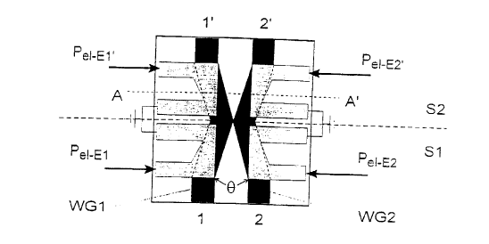
The multi-layer structure of a polymer-based digital optical switch
shown in Fig. 1 is provided in its input and output sections S1 and S2 with
S symmetrical waveguides of identical cross-section and refractive index. Two
input waveguides WG1 and WG2 with corresponding input gates 1 and 2 are
arranged at an angle O = 0.08~ in the input section S1. Waveguides WG1'
and WG2' with corresponding output gates 1' and 2' diverging from each
other at the same angle ~ are shown in the output section S2. The
20 waveguides in the input section S1 are arranged symmetrically with respect tothe waveguides in the output section S2. The waveguides were fabricated
from PMMA on a 3" Si wafer by standard polymer waveguide technology.
There cross-section measures 7 ,um x 7 I~m. The input and output
waveguides are spaced 250 ,um from each other. The overall length of the
~5 digital optical switch is 25 mm. Each of the four waveguides WG1, WG2,
WG1' and WG2' is taperingly superposed by an electrode E1, E2, E1' and
E2'. The propagation properties of light in the digital optical switch in
accordance with the Invention ~re characterized by an adiabatic mode
evolution. The conditions for the adiabatic mode evolution can be realized for
30 each waveguide WG1, WG2, WG1' and WG2' by energizing the
corresponding electrode E1, E2, E1' and E2'. As a result of the invention, a
Attorney Docket 980304 9
~ ..... _ , .. .. . . .
CA 02257533 1998-12-07
Dec Ofi 98 ll:lla Karl Hormann, Esq. 617-491-8877 p.lZ
digital optical switch having two inputs and two outputs can finally be
fabricated on a polymer basis.
In ~ig 2, t~ e 2x2 polymeric digital optical switch described supra in top
5 elevation is depicted in cross-section. A SiOx buffer layer is arranged on a Si
substrate which serves as a heat sink For the reduction of losses and for
protection against moisture, a 3 ,um thick buffer layer TB made of Teflon~ is
arranged on the waveguide layer W in which the waveguides WG1, WG2,
WG1' and WG2' are disposed. As a final layer, a corresponding heating
10 electrode E1, E2, E1' and E2' is arranged in superposition over each
wavegu;de WG1, WG2, WG1' and WG2' such that overlaps the waveguide in
a tapering manner.
The function of the DOS in accordance with the invention which is
15 based upon adiabatic mode evolution, may be described particularly well with
reference to Fig. 3 and Fig. 4. the first partial image of which depicts the input
and output sections S1, and S2 and the waveguides WG1, WG2, WG1' and
WG2' arranged in an X-shaped configuration. It also shows which electrode
is being heated. Th ensuing partial images depict the possible propagation of
20 a lightwave in the individual waveguides WG1, WG2, WG1', and WG2' in their
bar and cross states.
If as shown in Fig. 3, electrodes E2 and E2' are heated, i.e. if they are
energized by a power of Pel E2 and Pe, E2., the digltal optical switch will operate
25 in its bar state. As the light conducted into the unheated waveguide WG1
reaches the central region, the symmetric mode -as shown in the second
partial image- is conducted through waveguide WG1' which has a higher
index of refraction compared to waveguide WG2'. If light is conducted into
the heated waveguide WG2 the asymmetric mode will in the central region be
30 conducted into the waveguide WG2' which has a lower index of refractlon.
Between the unheated waveguide WG1JWG1' and the heated waveguide
Attorney Docket 980304 10
_, _ _ . . . . .
CA 02257533 1998-12-07
De~ O~ Y8 11: 12a Karl Hormann, Esq. 617-491-8877 p. 13
WG2NVG2' the difference in refractive index was found to be ~n - 0.0025.
If, as may be seen in the first partial image of Fig. 4, electrodes E1 and
E2" are heated, i.e., energized at a power of Pel E1 and E~ E2' the DOS in
5 accordance with the invention will operate in its cross state. In this case1 too,
the same difference in refractive index as mention abo\/e, was detected. If
li~ht is conducted into heated waveguide WG1 the asymmetric mode is
excited in the central region and the light will be conducted through the
heated waveguide WG2' which has the lower index of refraction. If light is
10 conducted tllrough the unheated WG2 the symmetric mode is excited in the
central region and light will be conducted through the waveguide WG1'. It
was found that the adiabatic mode can be maintained in the waveguides in
the input section as well as in the waveguides in the output section provided
that at an angle of ~3 s 0.1~ between the waveguides in the input or output
lS section the difference in refractive index is ~n ~ ~.0015
In order to characterize the polymeric digital optical switch in
accordance with the invention, the schematic structure and function of which
were explained in Figs. 1 and 2, and Figs. 3 and 4, respectively, light from a
20 laser diode at A = 1.55 ~Jm was coupled into the input gate 1 and into the input
gate Z, and the optical power POPt was measured at the output gates 1' and 2'.
Since it was found that the TE and TM polarization values were polarization
dependent by ctO,5 dB only, only the results for the TM polarization have
been indicated.
Fig. 5 thus shows the measurement trace of the transfer characteristic
at a wavelength of A = 1.55 ~m as a function of the electrical power P~l E~. i.e.,
in this case it was electrode E2' which was heated. The electrode E2 was
energized at a constant power Pe, E2, which in this case was 65 mW (the
30 energization is depicted in the inserted image). This is necessary in order to
realize the adiabatic mode evolution within waveguides WG1 and WG2 of the
Att~mey D~cket 980304 1 l
_ _ . . ...
CA 02257533 1998-12-07
Dec 06 98 11: lZa Karl Hormann, Esq. 617-491-8877 p. 14
input section 1. In this configuration the switch operates in its bar state. Thevalue measured for cross-talk was measured as c-25 dB at an electric
switching power of P~ E2 2 45 mW. It was found that this value does not
change for switching powers of Pel t2, 100 mW.
The transfer characteristic for a polyn~eric digital optical switch in
accordance with the invention as a function of electric power Pe, E2 for the
cross state is shown in Fig. 6. In the case, electrode E1 is energize~ by a
constant electric power Pel E1 = 45 mW in order again to satisfy the conditions
of adiabatic mode evolution in waveguides WG1 and WG2 of the input
section S1. If the variably adjustable switching power assumes values of
2 45 mW, here, too, the measured cross-talk was c-25 dB. The insignificant
deviation of the powers set as a constant in both described switching states
must be assumed to be the result of insignificant manufacturing differences in
the electrodes and waveguides. This does not, however, affect the principle
of the invention to structure each waveguide such that it is transparent to one
defined mode only
The switching time of the thermo-optical polymer DOS in both
switchlng configurations is c 1 ms.
The defined transfer characteristic in the sarne switch was also
established at A = 1.3 I~m and displays a similar digital switching action (not
shown).
Looking at Fig. 7 which depicts the transfer characteristics of the
polymer DOS in accordance with the invention with the same electrode
configuration as shown in Fig. 5 but at different values for Pel E2, it will be seen
that the switching action of such a DOS may be adjusted by energizing an
electrode in the input section at a ~/ariable switching power and by a constant
basic energization of an electrode in the input section. It can be seen that the"digitality" of the DOS may be adjusted as a function of the constant value
Attorney Docket 980304 12
CA 02257533 1998-12-07
Dec ora 98 1 1: 1 2a Kar 1 Hormann, Esq . 617-491 -8877 p . 15
Pe, E2 for the basic energization of electrode E2 in input section S1, such thatwithin a narrow range of Pe, E2, values a very good extinction ratio is ensured.If this value is changed a "robust" digital switching action at a low extinctionratio will present itself.
s
The described switching action permits tolerances in the technological
fabrication process and eliminates the need for a precise current or voltage
control. Furthermore, the switching action of the presented DOS is stable
against changes in ambient temperature.
Attomey Docket 980304 13
CA 02257533 1998-12-07