Language selection

Search

Patent 2257682 Summary

Third-party information liability

Some of the information on this Web page has been provided by external sources. The Government of Canada is not responsible for the accuracy, reliability or currency of the information supplied by external sources. Users wishing to rely upon this information should consult directly with the source of the information. Content provided by external sources is not subject to official languages, privacy and accessibility requirements.

Claims and Abstract availability

Any discrepancies in the text and image of the Claims and Abstract are due to differing posting times. Text of the Claims and Abstract are posted:

  • At the time the application is open to public inspection;
  • At the time of issue of the patent (grant).
(12) Patent Application: (11) CA 2257682
(54) English Title: FIBRE OPTIC MODULE
(54) French Title: MODULE A FIBRES OPTIQUES
Status: Deemed Abandoned and Beyond the Period of Reinstatement - Pending Response to Notice of Disregarded Communication
Bibliographic Data
(51) International Patent Classification (IPC):
  • G02B 6/42 (2006.01)
  • G02B 6/12 (2006.01)
(72) Inventors :
  • ISAKSSON, JAN (Sweden)
(73) Owners :
  • MITEL SEMICONDUCTOR AB
(71) Applicants :
  • MITEL SEMICONDUCTOR AB (Sweden)
(74) Agent: MARKS & CLERK
(74) Associate agent:
(45) Issued:
(22) Filed Date: 1998-12-31
(41) Open to Public Inspection: 1999-07-31
Examination requested: 1999-04-12
Availability of licence: N/A
Dedicated to the Public: N/A
(25) Language of filing: English

Patent Cooperation Treaty (PCT): No

(30) Application Priority Data:
Application No. Country/Territory Date
9802046.4 (United Kingdom) 1998-01-31

Abstracts

English Abstract


An optical module comprising an optoelectronic board having electrical
connection
sites for connection with an electrical circuit. The module includes a
plurality of
optoelectronic devices on the optoelectronic board and an optical fiber
connector including
a plurality of optical elements each for connection with a respective
optoelectronic device.
Cooperative alignment members on the optoelectronic board and the optical
fiber
connector are provided for aligning the optoelectronic devices on the board.


Claims

Note: Claims are shown in the official language in which they were submitted.

THE EMBODIMENTS OF THE INVENTION IN WHICH AN EXCLUSIVE
PROPERTY OR PRIVILEGE IS CLAIMED ARE DEFINED AS FOLLOWS:
1. An optical module, comprising in combination:
a circuit board having electrical connection means for connection to a further
circuit;
an optoelectronic device mounted on said board, said optoelectronic device
including first alignment means; and
an optical fiber connector including an optical element for connection with
said
optoelectronic device, said connector including second alignment means for
cooperative
engagement with said first alignment means, whereby said optoelectronic device
and said
optical fiber connector are aligned together when said alignment means are
engaged.
2. The optical module as set forth in claim 1, wherein said at least one
optoelectronic device comprises an optical die.
3. The optical module as set forth in claim 1, wherein said optoelectronic
device comprises super luminescence diodes, surface emitting diodes, vertical
cavity
surface emitting diodes and transceiving detectors.
4. The optical module as set forth in claim 1, wherein said second alignment
means comprises guide pins on said fiber connector.
5. The optical module as set forth in claim 1, wherein said module includes
a plurality of optoelectronic devices, said devices arranged in parallel
relation.
6. The optical module as set forth in claim 5, wherein each optoelectronic
device of said plurality of optoelectronic devices includes a semiconductor.
7. The optical module as set forth in claim 1, wherein said optical fiber
connector comprises a fiber ferrule.

8. An optical module, comprising:
a circuit board for receiving components;
an optical die component having a frame therearound and alignment means in
said
frame; and
an optical fiber ferrule component containing optic fibers and including
second
alignment means for cooperative engagement with said first alignment means and
for
ensuring alignment of said die and said ferrule on said board.
9. The module as set forth in claim 8, wherein said optical die includes a
vertical cavity surface emitting laser.
10. The module as set forth in claim 8, wherein said circuit board includes a
plurality of electronic components.

Description

Note: Descriptions are shown in the official language in which they were submitted.


CA 02257682 1998-12-31
FIBER OPTIC MODULE
The present invention relates to a fiber optic module and more particularly,
the
present invention relates to a module where a plurality of optical elements
may be
mounted to an optoelectronic board.
Interconnection of optical fibers to optoelectronic assemblies has always been
problematic in the art. Connection between the fibers and optoelectronic
devices is
important for efficiency in the transmission of wavelength and power.
Imprecise alignment
causes aberrations in these parameters.
In view of the alignment difficulties known in the art, existing modules
present
limitations in terms of high costs and providing alignment and mounting
optoelectronic
devices on a circuit board. The present invention addresses these difficulties
and in
accordance with one aspect provides an optical module, comprising in
combination:
a circuit board having electrical connection means for connection to a further
circuit;
an optoelectronic device mounted on the board, the optoelectronic device
including
first alignment means; and
an optical fiber connector including an optical element for connection with
the
optoelectronic device, the connector including second alignment means for
cooperative
engagement with the first alignment means, whereby the optoelectronic device
and the
optical fiber connector are aligned together when the alignment means are
engaged.
In a further aspect of one embodiment of the present invention, there is
provided
an optical module, comprising:
a circuit board for mounting components;
an optical die component having a frame therearound and alignment means in the
frame; and
an optical fiber ferrule component containing optic fibers and including
second
alignment means for cooperative engagement with the first alignment means and
for
ensuring alignment of the die and the ferrule on the board.

CA 02257682 1998-12-31
2
The present invention facilitates connection of a series of electrical,
optical or other
optoelectronic elements to a circuit board, which board may then be integrated
into a
larger circuit, etc. Alignment between optical fiber connectors and
optoelectronic devices
is ensured by employing optoelectronic devices having a frame or die with
alignment
apertures. These apertures cooperatively engage other alignment members which
may
comprise pins or projections associated with the fiber connector.
It will be understood that the pins/projections may be associated with the
optoelectronic device as an alternative. Further, loose pins may also be
employed for
connection within apertures provided in the optoelectronic device and
connector.
Having thus generally described the invention, reference will now be made to
the
accompanying drawings illustrating preferred embodiments and in which:
Figure 1 is a plan view of one embodiment of an optoelectronic board for use
with
the present invention;
Figure 2 is a plan view of a lead frame for a flip chip mounted optical die;
Figure 3 is a plan view of a lead frame for a flip chip mounted optical array;
and
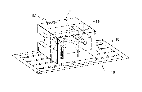
Figure 4 is a perspective view of one embodiment of a module in accordance
with
the present invention.
Similar numerals used in the text denote similar elements.
Referring now to the drawings, the electronic board 10 includes optoelectronic
devices 14 and other circuits (not shown) forming a module. The devices 14
each have
connection sites 18 for connection with an electrical circuit ( not shown ).
The electronic
board 10 includes alignment apertures 22 for alignment with optical elements
26 or 30

CA 02257682 1998-12-31
3
shown in Figures 2 and 3, respectively or for surface mounting of other
optoelectronic
devices.
Optical element 26 includes an optical die, e.g. a laser diode 34, having
contact
pads 38 and 42. A frame 36 surrounds die 34 and includes a lead frame 37. This
configuration facilitates flip chip bonding of the diode 34. Figure 3
illustrates an optical die
array. Each of the elements 26 and 30 include alignment apertures 46 and 48
for ensuring
alignment of the elements 26 and 30 with a fiber ferrule connector 52, shown
in Figure 4.
To this end, connector 52 includes guide pins 56 for cooperative engagement
within
apertures 46 and 48.
In terms of the optical elements, the same may comprise super luminescence
diodes, surface emitting diodes, vertical cavity surface emitting diodes as
well as others
known to those skilled in the art.
In addition to optoelectronic components, non-optical components may be
mounted commonly to the board 10 while facilitating alignment between ferrule
52 and
optical die 26.
In the case where the optical die array 30 is used, the ferrule 52 will carry
sufficient
optical elements for connection to a respective device.
Although embodiments of the invention have been described above, it is not
limited thereto and it will be apparent to those skilled in the art that
numerous
modifications form part of the present invention insofar as they do not depart
from the
spirit, nature and scope of the claimed and described invention.

Representative Drawing
A single figure which represents the drawing illustrating the invention.
Administrative Status

2024-08-01:As part of the Next Generation Patents (NGP) transition, the Canadian Patents Database (CPD) now contains a more detailed Event History, which replicates the Event Log of our new back-office solution.

Please note that "Inactive:" events refers to events no longer in use in our new back-office solution.

For a clearer understanding of the status of the application/patent presented on this page, the site Disclaimer , as well as the definitions for Patent , Event History , Maintenance Fee  and Payment History  should be consulted.

Event History

Description Date
Time Limit for Reversal Expired 2003-12-31
Application Not Reinstated by Deadline 2003-12-31
Deemed Abandoned - Conditions for Grant Determined Not Compliant 2003-02-10
Deemed Abandoned - Failure to Respond to Maintenance Fee Notice 2002-12-31
Notice of Allowance is Issued 2002-08-08
Letter Sent 2002-08-08
Notice of Allowance is Issued 2002-08-08
Inactive: Approved for allowance (AFA) 2002-07-31
Amendment Received - Voluntary Amendment 2002-06-18
Inactive: S.30(2) Rules - Examiner requisition 2002-06-05
Inactive: Cover page published 1999-08-06
Letter Sent 1999-08-03
Application Published (Open to Public Inspection) 1999-07-31
Inactive: Single transfer 1999-07-07
Amendment Received - Voluntary Amendment 1999-05-18
Letter Sent 1999-05-07
Request for Examination Received 1999-04-12
Request for Examination Requirements Determined Compliant 1999-04-12
All Requirements for Examination Determined Compliant 1999-04-12
Inactive: IPC assigned 1999-02-19
Classification Modified 1999-02-19
Inactive: First IPC assigned 1999-02-19
Inactive: IPC assigned 1999-02-19
Inactive: Correspondence - Formalities 1999-02-16
Inactive: Filing certificate - No RFE (English) 1999-02-05
Filing Requirements Determined Compliant 1999-02-05
Application Received - Regular National 1999-02-03

Abandonment History

Abandonment Date Reason Reinstatement Date
2003-02-10
2002-12-31

Maintenance Fee

The last payment was received on 2001-12-18

Note : If the full payment has not been received on or before the date indicated, a further fee may be required which may be one of the following

  • the reinstatement fee;
  • the late payment fee; or
  • additional fee to reverse deemed expiry.

Please refer to the CIPO Patent Fees web page to see all current fee amounts.

Fee History

Fee Type Anniversary Year Due Date Paid Date
Application fee - standard 1998-12-31
Request for examination - standard 1999-04-12
Registration of a document 1999-07-07
MF (application, 2nd anniv.) - standard 02 2001-01-01 2000-10-11
MF (application, 3rd anniv.) - standard 03 2001-12-31 2001-12-18
Owners on Record

Note: Records showing the ownership history in alphabetical order.

Current Owners on Record
MITEL SEMICONDUCTOR AB
Past Owners on Record
JAN ISAKSSON
Past Owners that do not appear in the "Owners on Record" listing will appear in other documentation within the application.
Documents

To view selected files, please enter reCAPTCHA code :


To view images, click a link in the Document Description column. To download the documents, select one or more checkboxes in the first column and then click the "Download Selected in PDF format (Zip Archive)" or the "Download Selected as Single PDF" button.

List of published and non-published patent-specific documents on the CPD .

If you have any difficulty accessing content, you can call the Client Service Centre at 1-866-997-1936 or send them an e-mail at CIPO Client Service Centre.


Document
Description 
Date
(yyyy-mm-dd) 
Number of pages   Size of Image (KB) 
Representative drawing 1999-08-06 1 13
Abstract 1998-12-31 1 14
Description 1998-12-31 3 113
Claims 1998-12-31 2 52
Drawings 1998-12-31 2 48
Cover Page 1999-08-06 1 35
Drawings 1999-02-16 2 40
Claims 2002-06-18 1 40
Filing Certificate (English) 1999-02-05 1 163
Acknowledgement of Request for Examination 1999-05-07 1 179
Courtesy - Certificate of registration (related document(s)) 1999-08-03 1 139
Reminder of maintenance fee due 2000-09-05 1 110
Commissioner's Notice - Application Found Allowable 2002-08-08 1 164
Courtesy - Abandonment Letter (Maintenance Fee) 2003-01-28 1 176
Courtesy - Abandonment Letter (NOA) 2003-04-22 1 166
Correspondence 1999-02-09 1 33
Correspondence 1999-02-16 3 62