Note: Descriptions are shown in the official language in which they were submitted.
CA 02257900 1998-12-10
WO 97/48102 1 PCT/SE97/00979
A method and device for processingsampled analogue signals in
digital BiCMOS process
The present invention relates to a method for processing sampled
analogue signals in a digital BiCMOS process and a device for
processing sampled analogue signals in a digital BiCMOS process.
~ackgrn"nr~ of the invention
The switched current (SI) technique is a relatively new analog
sampled data signal processing technique, that fully exploits
digital CMOS technology, see for example "Switched currents, an
analogue technique in digital technology" by C. Toumazou, J.B.
Hughes and N.C. Battersby, Peter Peregrinius Ltd, 1993. The
ultimate performance of the SI circuits is primarily determined
by the transconductance gm of an MOS transistor and the
capacitance Cg seen by its gate. Although a high speed operation
(around 100 Mhz) is possible, the performance of speed and
accuracy is limited by the technique itself . In order to have
high accuracy, large Cg is usually required, since the clock
feedthrough error is inversely proportional to Cg. Therefore,
increasing g~ is the only way to increase the speed. With the
same bias current, the transconductance of an MOS transistor is
considerably lower than that of a bipolar transistor. Therefore,
utilization of the bipolar transistor could increase the speed
and/or improve the accuracy. BiCMOS technology opens the
possibility of using both MOS and bipolar transistors.
A technique has been proposed for a high speed sampled-data
signal processing in BiCMOS, see for example "A new BiCMOS
technique for very fast discrete time signal processing" by P.
Shak and C. Toumazou in Proc. 1995 International Symposium on
Circuits and Systems pp. 323-326. It breaks the limitation of
gm/Cg of the SI circuits by utilizing bipolar transistors. It
CA 02257900 1998-12-10
WO 97/48102 2 PCTlSE97/00979
first converts a current to a voltage by a transresistor and
then converts the voltage to a current by a transconductor. The
voltage is sampled and held at the input of the transconductor,
whose input device is an MOS transistor. However, the conversior_
accuracy is determined by the absolute value of the components.
For example, the resistor determines the transresistance value,
and the transistor size and the operation condition determine
the transconductance value. Therefore the technique is sensitive
to process variation and another drawback is its complexity.
Patent applications have been filed by John B. Hughes of
Philips, U.K. on a technique, which was referred to as the
switched-current technique, see for example EP 89203067.7, 1989-
12-04. All these applications were concentrated on the technique
for a digital CMOS process.
Summary of the invention
In a digital BiCMOS process the storage capability of MOS
transistors and the large transconductance of bipolar
transistors can be utilized in such a way, that the speed is
primarily determined by the capacitance seen by the MOS
transistor and the transconductance of the bipolar transistor.
The advantages over the prior SI technique in CMOS are higher
speed, smaller errors, and higher accuracy. The advantages over
other techniques in BiCMOS such as mentioned in the background
of the invention are smaller errors and higher accuracy. The
unique feature of the invented technique is the combination of
high input impedance of the MOS devices and high
transconductance of the bipolar devices, where both devices are
only available in BiCMOS process and not in the CMOS process.
CA 02257900 1998-12-10
WO 97/48102 3 PCT/SE97/00979
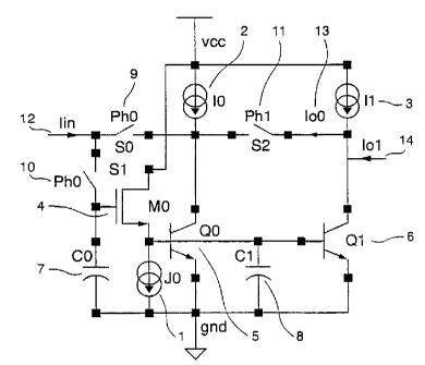
Figure 1 is a circuit configuration of the proposed technique
according to the invention.
Figure 2 is an alternative circuit configuration of the proposed
technique according to the invention.
Figure 3 shows a simulated response of the circuit of figure 1.
Figure 4 shows simulated errors versus input currents according
to the invention.
The proposed new technique utilizes a composite transistor
consisting of an MOS transistor and a bipolar transistor. The
MOS transistor is in common-drain configuration and the bipolar
transistors are in common-emitter configuration as shown in Fig.
1. Current sources JO 1, IO 2 and I1 3 provide bias currents for
transistors MO 4, QO 5 and Q1 6, respectively. A capacitor CO 7
represents all the capacitance at the gate of the transistor MO
and C1 8 represents all the capacitance at the source of the
transistor M0.
All the switches are controlled by a non-overlapping clock.
During clock phase PhO, switches SO 9 and S1 10 are closed, and
S2 11 is open. The input current Iin 12 flows into the collector
of the transistor QO and makes the base-emitter voltage change
correspondingly. Due to the common-drain configuration of the
transistor M0, its gate source voltage does not change, the
potential at the gate of the transistor MO changes
proportionally as well. When the stable condition is reached, a
potential at the gate of the transistor MO is created to change
CA 02257900 1998-12-10
WO 97/48102 4 PCT/SE97/00979
the base-emitter voltage of the transistor QO to sink (or
source) the input current into the transistor Q0. Since the
transistors QO and Q1 have the same base-emitter voltage, the
output current Iol 14 is equal to the input current Iir_, if the
two transistors have the same emitter area.
During clock phase Phl, the switches SO and S1 are open and S2
is closed. The gate of the MOS transistor MO is isolated and the
potential at the gate is held. Since the gate source voltage of
the transistor MO is constant, the base-emitter voltage of the
transistor QO does not change. Therefore, the collector current
of the QO does not change. The output current Io0 13 is equal to
the input current Iin, that was the input into the transistor QO
during the clock phase PhO. Since the transistors QO and Q1 have
the same base-emitter voltage, the output current Iol is equal
to the output current IoO, if the two transistors have the same
emitter area.
Therefore, the output current Io0 is the memory of the input
current Iin and the output current Iol realizes the track-and-
hold function performed on the input current Iin. Since same
devices as MO and QO are used both as input and as output
devices, there is no mismatch between input current Iin and the
output current IoO, just as in a second-generation SI memory
cell. A scaling factor between the output current Iol and the
input current Iin can be realized by choosing a different
emitter area.
The speed of the circuit is determined by the settling time when
the switches SO and S1 are closed. Neglecting the switch-on
resistance of the switch transistors, the system is a two-pole
system. The dominant pole frequency c.~o is equal to gmQo/C0,
1
CA 02257900 1998-12-10
WO 97/48102 5 PCT/SE97100979
where gmQO is the transconductance of the bipolar transistor QO
and CO is the total capacitance at the gate of M0. The non-
dominant pole frequency con is equal to g",r,~o/C1, where g,r,Mois the
transconductance of the MOS transistor MO and C1 is the total
capacitance at the source of the transistor M0.
For SI circuits in the CMOS process, the dominant pole frequency
is determined by the total capacitance seen by the gate of the
MOS transistor and the transconductance of the MOS transistor.
Due to the higher transconductance of bipolar transistor, the
proposed technique has a superior speed performance if the non-
dominant frequency is sufficiently high. This can be satisfied
in circuit design by minimizing the capacitance at the source of
M0, especially when a reasonably large capacitance CO is used to
reduce clock feedthrough errors.
Speed could also be traded off for accuracy by using a large
capacitance C0, since the clock feedthrough error is inversely
proportional to the C0. Also due to the use of the bipolar
transistor, the voltage change at the gate of the MO is small
even with. large input currents, which reduces the signal
dependent clock feedthrough errors. Another source of errors in
the SI circuits in the CMOS process is due to the drain-gate
parasitic capacitance. When the drain potential changes, it
couples into the gate through the drain-gate parasitic
capacitance, which introduces excessive errors, especially for
high frequency applications. In the proposed circuit shown in
Fig. 1, the drain potential of the MOS transistor is tied to Vcc
and, therefore, during switching the gate voltage is not
influenced. Therefore, the proposed technique has much smaller
errors, both signal dependent and signal independent errors.
CA 02257900 1998-12-10
WO 97/48102 6 PCT/SE97/00979
The devices MO and QO are used both as input and as output
devices as in second-generation SI memory cells in the CivIOS
process, mismatch does not introduce any error. However, in most
cases current mirrors are needed to realize different
coefficients as in the case of using transistor Q1 and mismatch
plays an important role. Since the bipolar transistor matching
is better than the MOS transistor matching, the proposed
technique is also superior to the SI technique in CMOS process
concerning accuracy.
Finally, it is worthwhile to note the simplicity. Since bipolar
transistors have larger early voltages and the potential change
at the collector of the QO is small during the input and output
stages, the circuit illustrated in Fig. 1 can function well
without further elaboration. In principle, the SI circuits are
simple in the CMOS process too. However, to deal with different
errors, e.g. clock feedthrough errors, limited input/output
conductance ratio errors, the errors due to the gate-drain
parasitic capacitance, relatively complex circuits and/or
clocking are needed. The proposed technique does not require
linear capacitors as the SI technique in the CMOS process.
Compared with the technique earlier proposed, the new technique
does not demand matching between a transresistor and
transconductor and the circuit scheme is much simpler.
An alternative circuit realization is shown in Fig. 2. It bears
resemblance to the first-generation SI memory cell in the CMOS
process. In Fig. 2 different devices are used for input and
output. The transistors MO 15 and QO 16 are used as input
devices, and the transistors M1 17 and Q1 18 are used as output
devices. Current sources JO 19, IO 20, J1 21 and I1 22 provide
bias currents for transistors M0, Q0, M1 and Q1, respectively.
_ _ ____ ... . . 1
CA 02257900 1998-12-10
WO 97/48102 -7 PCT/SE97/00979
The capacitor CO 26 represents all the capacitance at the gate
of transistor M0. The capacitor C1 27 represents all the
capacitance at the source of transistor M0. The capacitor C2 28
represents all the capacitance at the gate of transistor M1. The
capacitor C3 29 represents all the capacitance at the source of
transistor M1.
Suppose the transistors MO and M1 have the same size and the
transistors QO and Q1 have the same size. During the clock phase
Ph0 when the switch SO 23 is closed, the gate voltage of the M1
is equal to that of the MO and therefore the base emitter
voltages of the transistors QO and Q1 equal. This makes the
collector currents of the QO and Q1 equal. Therefore the output
current Io 24 is equal to the input current Iin 25. During the
clock phase Phl when switch the SO is open, the gate of M1 is
isolated and the potential is held. This makes the base-emitter
voltage of the Q1 constant and therefore the collector current
is constant. The output current Io is held constant. Therefore,
the circuit realizes a track-and-hold function just as the
first-generation SI memory cell in CMOS process. This circuit
shows superior performance over its CMOS counterparts just as
outlined above.
In order to verify the functionality, the circuit shown in Fig.
1 is simulated by using parameters of a 3.3-V digital BiCMOS
process. The supply voltage is 3.3 V. The input current Iin and
output current Iol are shown in Fig. 3. The input current is a
20-MHz 100-uA sinusoidal and the clock frequency is 100 MHZ. It
is evident that a track-and-hold function is realized.
In Fig. 4 the simulated current errors are shown versus input
currents of a fully differential design based on the circuit
scheme shown in Fig. 1. The bias current in each branch is about
CA 02257900 1998-12-10
WO 97/48102 g PCT/SE97/00979
360 uA. It is seen that when the sampling frequency is 100 Mhz,
the error is less 0.55% and the variation is small. This
indicates good linearity. When the clock frequency increases to
250 MHz, the error increases due to the settling error. The
error variation is still small when the input current is less
than 50% of the bias current, indicating good linearity.
While the foregoing description includes numerous details and
specificities, it is to be understood that these are merely
illustrative of the present invention, and are not to be
construed as limitations. Many modifications will be readily
apparent to those skilled in the art which do not depart from
the spirit and scope of the invention, as defined by the
appended claims and their legal equivalents.
T