Note: Descriptions are shown in the official language in which they were submitted.
CA 022~799~ 1998-12-11
WO 97/48241 PCT/EP97/02977
OPTICAL SWITCH MATRIX
The invention pertains to an optical switch matrix comprising n input
channels, branching means for dividing the input channels up into a total of
5 p branched channels, merging means for merging p branched channels
into m output channels, and optical fibres for connecting the output
channels of the branching means with the input channels of the merging
means, wherein n, m, and p are natural numbers greater than or equal to 2.
10 Such optical switch matrices are known. On February 10, 1995, during a
workshop of Eindhoven University of Technology in the Netherlands
Siemens presented an 8x8 optical switch matrix named "8x8 Modulaufbau,"
which consists of an array of sixteen juxtaposed 1x8 switches on a long
rectangular InP-substrate and optical fibres (embedded in a product of
15 AT&T called "OptiflexTM" and bent through an angle of 180~) for connecting
the switches. Eight of said 1x8 switches are each used as an input channel
which branches into in eight channels. Each of these branched channels is
connected to one of the merging channels of the remaining eight 1x8
switches (or, more accurately, 8x1 switches), in such a manner that an
20 input signal in one of the input channels can be switched to any one of the
output channels.
Said optical switch matrix has a length of more than 300 mm and a width of
at least 50 mm, which is very large, especially in an industry where small
25 size is, in many cases, of the essence. A reason for these considerable
dimensions is that the optical fibres, which are usually made of glass, can
only be bent to a certain extent. The minimal bending radius for glass fibres
is about 25 mm. If smaller radii are used, the glass fibre may break or the
optical loss within the fibre may increase to an unacceptably high level. As
30 mentioned, in said optical switch matrix the fibres are bent through an
_ . . . . . . .
CA 022~799~ l998-l2-ll
WO 97/48241 PCT/EP97/02977
angle of 180~. Consequently, the minimum width of the matrix exceeds 50
mm. The present invention has for its object to provide an nxm optical
switch matrix which is relatively small in size. To this end, an optical switch
- matrix as described in the first paragraph is provided wherein the branching
5 means, the optical fibres (preferably p in all), and the merging means are
each attached to a separate sulJsl~dte or a separate group of substrates,
which substrates are optically aligned.
Surprisingly, it has been found that the present invention allows a size
10 reduction of the order of 80%. The use of a separate substrate for the
optical fibres enables very efficient placement thereof, resulting in a
considerable size reduction both in the longitudinal and the transverse
direction, especially if the substrate with the branching means and the
substrate with the merging means are on opposite sides of the substrate to
15 which the optical fibres are attached. Further, owing to the compactness
and rigidity of the elements of the optical switch matrix according to the
invention, said elements can be aligned accurately with relatively little effortand do not suffer from tensions induced by movement of the optical fibres
during operation (as can be the case with structures such as "OptiflexTM").
Usually, switch matrices are packaged in a hermetically sealed unit to
protect them from corrosion. Said small size of the matrices according to
the invention allows the use of a single package unit or box for packaging
the entire switch matrix. In consequence, only n+m fibres have to be fed
25 through the walls of the package. Up until now, the branching means and
the merging means were each packaged in one or more separate boxes,
and the optical fibres emerging from these boxes were spliced together one
by one. In that case, the total number of fibre feedthroughs amounts to
n+m+2p.
CA 022~799~ 1998-12-11
WO 97/48241 rCT/EP97/02977
For a 8x8 switch matrix, the invention makes it possible to reduce the total
number of fibre feedthroughs from 144 (i.e., 8+8+(2x64)) to 16 (i.e., 8+8),
which since the hermetic feedthroughs are responsible for the greater part
of total packaging costs, is a major advantage. Also, instead of the
5 interconnect fibres and the fibres extending from the merging/branching
means being spliced together one by one, the substrates according to the
invention (provided with the interconnect fibres and the merging/branching
means, respectively) can be optically aligned in a few automated process
steps using conventional equipment.
Further, the invention solves another problem inherent to the above
mentioned "8x8 Modulaufbau" which resides in the fact that the dimensions
of the substrates carrying the switches or optical fibres are, of course,
limited by the dimensions of the wafers of which the substrates are made.
15 If, for instance, InP-wafers are used, the maximum length of the InP-
substrates is 2 inches at most because InP-wafers have (at present) a
maximum diameter of 2 inches. Since 8 1x8 switches need a total length of
about 1 inch, the number of juxtaposed 1x8 switches on a single substrate
cannot exceed 16. Consequently, larger matrices, e.g., 16x16 matrices
20 which would comprise 32 juxtaposed switches, cannot be manufactured
using the "8x8 Modulaufbau," whereas they can be manufactured using the
present invention.
It will be understood that, apart from the above example, the invention
25 allows the construction of larger matrices with at least a double switch
capacity irrespective of the material used.
The terms "branching means" and "merging means" include both active
means (e.g., switches) and passive means. Since the invention pertains to
30 a switch matrix, the total number (and the position) of the switches in the
CA 022~799~ 1998-12-11
WO 97/48241 PCTIEP97/02977
branching means and the merging means should be such that at least two
input channels can selectively be connected (for a certain wavelength) to
one of at least two output channels.
Optical switch matrices wherein n (the number of inputs) and m (the
number of outputs) are equal or wherein n equals 2m or ml2 are preferred.
Such matrices can be mass-produced, are very versatile, and, more
importantly, are basic building blocks in telecommunications and Clos
networks. Preferred are those optical switch matrices wherein n equals 2i,
"i" being an integer (preferably in the range of 2-8, at present more
preferably 2-5), and/or wherein said branching means and said merging
means consist of a c~sc~de ortree of 1x2 and 2x1 switches, respectively.
It should be noted that although it is, in some cases, preferred to integrate
all branching or merging means on a single substrate (which allows simple
production and optical alignment of the separate substrates), the invention
does not exclude the use of more than one substrate for each of said
means. For example, a 4x4 matrix comprising 4 branching means (4 1x4
switches) each on a separate subst~dte, an interconnect chip provided with
16 optical fibres, and 4 merging means (4 4x1 switches) arranged in twos
on two substrates, is also within the scope of the present invention. By
doing so, defective switches can be disposed of individually instead of in
combination with the sound switches on the same substrate. Thus, the
production yield is improved.
In a preferred embodiment, the optical fibres are attached to a substrate
with at least p grooves on two opposing sides. This can be achieved, for
instance, by providing short grooves on both sides or by providing grooves
which run the length of the sub~lldte. The substrates can be manufactured
CA 022~799~ 1998-12-ll
WO 97/48241 PCT/EP97/02977
using conventional methods and enable aulo"lated and accurate
placement of the fibres, again using conventional techniques.
In principle, the substrates can be made of any material suitable for
supporting a polymeric waveguide structure or optical fibres. In connection
5 with the alignment of the optical fibres with the channels of the switches, itis preferred to use rigid materials. Examples are thermoset polymers (in
which the desired grooves can be made, e.g., by shaping techniques such
as injection moulding), glass, or other inorganic materials such as silicon,
alloys consisting for the greater part of silicon, or GaAs and the like. In the
10 last of these materials, grooves can be made by etching techniques known
from the semiconductor industry. The grooves preferably are V-shaped,
thus providing two facets vis-à-vis which the optical fibres can be kept very
tightly in place and allowing most accurate positioning in respect of the
waveguide facets.
If use is made of single mode fibres, which have a core diameter of about
10 microns and an outer diameter of about 125 microns, the substrate
preferably is a monocrystalline material exhibiting an anisotropic etching
characteristic, since such materials allow very accurate definition of the
20 dimensions of the V-grooves which will contain the fibres. In this respect
silicon, alloys consisting for the greater part of silicon, and indium
phosphide are examples of suitable and preferred substrate materials.
In order to allow very accurate alignment of the optical fibres with the inputs
25 and outputs of the optical switches, at least the substrate to which the
optical fibres are attached has a surface flatness of less than 3 microns,
preferably less than 2 microns, at least near the endfaces. This can, for
instance, be achieved by using a substrate of which the entire surface
meets said flatness, by polishing the substrate near the endfaces, or by
, . . . . ..
CA 022~799~ 1998-12-ll
WO 97/48241 PCT/EP97/02977
glueing pieces of material having said flatness to the substldte, again at
least near the endfaces of the substrate.
The aforementioned optical switches can, for instance, be thermo-optical
5 (TO), electro-optical (EO), magneto-optical (MO), acousto-optical (AO) or
mechano-optical switches. Suitable examples of thermo-optical switches
are described in European patent applications 95200965.2, 95201460.3,
and 95201762.2, all in the name of Akzo Nobel NV. The invention of
course is not restricted to certain optical materials. However, for an
10 example of a suitable material reference is made to European patent
application 95201761.4 in the name of Akzo Nobel.
It is noted that in R.A. Spanke, "Architectures for Large Nonblocking Optical
Space Switches," IEEE Journal of Quantum Electronics, Vol. QE-22, No. 6
15 (June 1986), 964-967 a drawing is shown of an nxn optical switch matrix
wherein splitter and combiner means are in a direct line. The drawing is of
a purely schematic nature and does not suggest the use of a separate
substrate for the optical interconnect fibres, which substrate is essential to
the present invention.
P. Granestand, et al., "Integrdled Optics 4 x 4 Switch Matrix with Digital
Optical Switches," Electronic Letters, Vol. 26, No.1, 4th January 1990,
discloses a 4x4 optical switch matrix wherein all the elements, i.e. 1x4
switches and interconnect waveguides, are built on a single substrate.
WO 96/08932 describes an 8x8 optical switch matrix only in principle, the
actual construction of the matrix is not disclosed.
The invention will now be illustrated by way of an unlimitative example.
CA 022~799~ 1998-12-11
WO 97148241 PCT/EP97/02977
E)(AMPLE
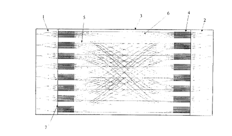
The Figure shows two chips (1,2) each provided with eight 1x8 thermo-
optical switches (ex Akzo Nobel, type Beambox Technology; length: 50
5 mm, width: 27 mm), an "input" chip (1 ) and an "output" chip (2). An
interconnect chip (3) (length: 30 mm, width: 27 mm) is made of silicon 100
and is provided with 64 V-grooves (4) (obtained by anisotropic etching with
KOH-IPA etchant) spaced 250 I~m apart on both of its short sides.
10 To obtain the interconnect chip (3) single mode optical fibres (5) (ex
Corning), of which the acr,vlate coating is removed only in the areas which
are intended to be placed in the V-grooves (4), are mounted on the
subsl~ate (6) as depicted in the Figure and fixed in the V-grooves with a
UV-curing adhesive. A glass plate provided with a UV-curing adhesive on
15 one side is placed on top of the fibres and the thus obtained stack of glass
plate, optical fibres (5), and substrate (6) is cured and then diced in one
step so as to obtain the endfaces (7) of the interconnect chip (3).
Subsequently, the chips (1,2) provided with the 1x8 switches and the
20 interconnect chip (3) are optically aligned in a conventional manner (active
alignment) and fixed.
As is clear from the above Example, the obtained 8x8 optical switch matrix
is extremely compact. Further, none of the optical fibres (5) have a bending
25 radius smaller than 25 mm.