Note: Descriptions are shown in the official language in which they were submitted.
CA 022~8279 1998-12-23
W 097J49987 PCT~US97111211
}-IIGH THROUC~nPUT SCREENING M ETHOD A~nD ~ PARATUS
Field of the Invention
The present invention relates to high throughput screening (HTS) methods, e.g., for
detecting the effect of a given compound or treatment on cell me~aholic activity, and apparatus
for performing such screening.
Back~round nf the Invention
With the advent of combinatorial library methods for generating large libraries of
compounds, there has been a growing interest in high-throughput screening (HTS) methods for
screening such libraries.
The most widely used HTS screening method involves competitive or non-competitive
binding of library compounds to a selected target protein, such as an antibody or receptor.
Thus, for example, to select a library compound capable of blocking the binding of a selected
agonist to a receptor protein! the screening method could assay for the ability of library
compounds to displace radio-labeled agonist from the target protein.
Although such binding assays can be used to rapidly screen large numbers of compounds
for a selected hinding activity, the assay itself may have limited relevance to the actual biologi-
cal activity of the compollnd in vivo, e.g., its ability to interact with and affect the metabolic
behavior of a target cell.
It would theretore be useful to provide high throughput screening methods capable of
testing the eftects of large numbers of lihrary compounds on target cells of interest.
Summary of the Invention
The invention includes, in one aspect~ high throughput screening apparatus, e.g., for
screening the effect ot test coml~ounds on cell metabolic activity, or for screening the effect of
a genetic manipulatinns on cells. The apparatus includes a multiwell device defining a plurality
of discrete microwells on a substrate surface, at a well density of greater than about 100/cm7,
where the well volumes are such as to accommodate at most ahout 106 cells/well, preferably
between 1-100 wells/ce]l, and structure for measuring the conductance in each well. The
measuring structure includes (i) a pair of electrodes adapted for insertion into a well on the
substrate~ and tii) circuitry for applying a low-voltage, AC signal across the electrodes, when
the electrodes are submerged in the medium, and for synchronously measuring the current
across the electrodes, to monitor the level of growth or metabolic activity of cells contained in
the chamber.
In various preferred emhodiments, the signal circuitry is effective to generate a signal
whose peak-to-peak voltage is hetween S and- 10 mV~ and includes feedback means t'or
adjusting the signal voltage level to a selected peak-to-peak voltage between 5 and 10 mV.
CA 022~8279 1998-12-23
WO 97149987 PCT/US97/1121~
In other embodiments, the circuitry is designed to sample the voltage of the applied signal
at a selected phase angle of the signal, or alternatively, to sample the voltage of the applied
signal at a frequency which is at least an order of magnitude greater than that of the signal.
In another general aspect, the invention includes a high-throughput screening method, e.g.,
for screening the effect ot test compounds on cell metabolic activity, or the effect of a given
genetic manipulation. The method includes placing cells in the wells of a multiwell device
defining a plurality of discrete microwells on a substrate surface, at a well density of greater
than about 100/cm2, with the number of cells in each well being less than about 10~, and prefe-
rably between 1-103. The coll~iuct~nce in each well is determined by applying a low-voltage,
AC signal across a pair of electrodes placed in that well, and synchronously measuring the
conductance across the electrodes.
These and other objects and features of the invention will become more fully ap~,arenl
when the tollowing detailed description of the invention is read in conjunction with the
accompanying drawings.
IS Brief Description of the Drawings
Fig. I is a perspective view of a multiwell device that forms part of the apparatus of the
invention;
Fig. 2A is an enlarged, tr~gment~ry cross-sectional view of the device in Fig. 1, with the
wells in the device each containing a small number of cells suspended in a culture medium;
Fig. 2B is a view like that in Fig. 2A, but further showing an electrode cover on the
device;
Fig. 3 illustrates the grid of conductive wires in the electrode plate shown in Fig. 2B;
Figs. 4A-4C illustrate another embodiment of the apparatus, here designed for well-by-well
conductance measurements;
Fig. 5 shows idealized plots of conductance, as a function of time, in the presence and
absence of a library compound that inhibits ce]l growth or metabolism;
Fig. 6 is a block diagram depicting selected portions of the data acquisition board and of
the measurement input/output board in accordance with the present invention; andFig. 7 depicts waveforms for the alternating current voltage supplied for application across
a pair of pins, an output signal produced by a col,-pal a~Or in response to the alternating current
voltage, and a hypothetical output signal from a sample-and-hold amplifier.
Detailed Description of the Invention
A. Screening Apparatus and Method
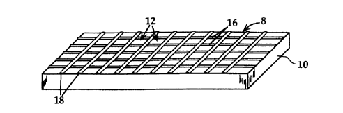
Fig. I shows a perspective view of a multiwell device 8 forrned of a substra~e 10
having a plurality of microwells, such as wells 12, on the upper substrate surface 14. In the
CA 022~8279 1998-12-23
W 097/4g987 rCTAUS97111211
embodiment shown, the microwells are forrned by a grid of hydrophobic lines, such as lines
16 extending lengthwise, and lines 18 extending widthwise. The lines are preferahly formed
of a hydrophobic polymer ma~erial, such as polyethylene or polystyrene, and are laid down in
a conventional manner, e.g., deposition of melted polymer from an applicator, or heat-mediated
5 ~t~chment of a polymer grid fabric directly to the substrate surface.
Spacing between adjacent parallel lines is preferably 20-200 ~m, so that the wells formed
by intersecting lines have area dimensions of between about 400 to 40,000 tlm2. The density
of wells on the substrate is at least 100/cm2 and more preferably 103/cm2 to 10~1cm or greater.
The height (surface relief) of the grid lines, seen best in Figs. 2B and 2B, is typically
between 20-200 ~m. Microwell volumes, defined by the volume that can be held as a discrete
droplet in a microwell, are typically in the range 10-4 to 2 nanoliters.
The microwells in the device may be filled with selected biological cells by applying a
suspension of the cells, at a desired cell density, over the device's surface, and allowing excess
suspension fluid to drain off, e.g., by blotting the edges of the device. This is illustrated in
15 Figs. 2A and 2B which show cell suspension droplets, such as droplet 20, in the microwells
of the device, such a~ microwell 22. It will be appreciated that the droplet meniscus may
extend above the height of the grid lines.
The cell density is adjusted so that the wells are filled, on average, with a selected number
of cells which is pre~erably between 1-~00, but may be as high as 103 per well. As illustrated
20 in Figs. 2A and 2B, the density of the cells is such that the device has an average of about 2
cells/well. A greater number of cells/well, e.g.. an average of 10-100/well provides improved
statistical correlation among events observed in different cells, due to more uniform cell-
number distribution in the microwells of the device. At the same time, a small number of
cells, e.g., 10-100. allows a microwell (microvolume) format in which desired concentrations
25 of test compounds can be achieved with very small amounts of compound, e.g., in the
femptogram to nanogram range. The actual number of cells employed will depend on the
particular type of cell and medium, and the confluency requirements of the cells.
With reference particularly to Fig. 2B, the apparatus of the invention, further includes
means for measuring the cor-duct~nce of the cell medium in each well. In the embodiment
30 shown, this means includes a multi-electrode cover 27 having a plurality of electrodes pairs,
- such as electrode pair 26 made up of electrodes 26a, 26b formed as a grid on the lower side
of the cover. Specifically, the grid of electrode pairs matches that of microwells in device 8,
~ so that placement of the cover on the device places an electrode pair in each microwell.
The measuring means also includes a signal unit 28 electrically connected to the cover as
35 described below with reference to Fig. 3. The operation of the unit to provide a low-voltage
CA 022~8279 1998-12-23
WO 97/4 m 7 PCTrUS97/11211
AC signal to each electrode, and interrogate the electrode to determine the conductance in each
microwell is described below with reference to Figs. 6 and 7.
Fig. 3 is a plan view of cover 27, showing the grid pattern of conductive wires, such as
longitudinal wires 30, and lateral wires 32, connecting the electrode pairs in the cover. Each
5 longitudinal wire is connected to an electrode connector, such as wires 32 connected to cormec-
tors 34, in a multi-connector array 36 along one side of the cover, as shown. Similarly, each
lateral wire is connected to an electrode connector, such as wires 32 connected to connectors
38, in a multi-connector array 40 along another side of the cover. The two arrays are designed
to plug into matching ports in the signal unit.
As seen in Fig. 2B, each longitudinal wire. such as wire 30, is electrically connected to
one of the two electrodes in the longitudinal one-dimensional array of electrode pairs, such as
the array including pair 26, adjacent the wire. Similarly, each lateral wire, such as wire 36,
is electrically connected to one of the two electrodes in the lateral one-dimensional array of
electrode pairs, such as the array including pair 26, adjacent that wire.
Thus, to interrogate a particular microwell in the device, the signal unit applies a low-
voltage signal across the two connectors in cover 27 which are connected to the two electrodes
in that well. For example, to interrogate microwell 26 in Fig. 2B, the signal unit applies a
voltage signal across connectors 34, 38 connected to electrodes 26a, 26b, respectively, forming
the electrode pair in that microwell. To this end, the signal unit includes the basic electronics
20 for applying a low-volta~e signal to the electrodes, and for synchronously measuring the
current across the electrodes, as described helow.
Unit 28 also includes conventional multiplexing or sampling circuitry for alternately and
successively interrogating each microwell, by applying a short duration signal to successively
to each well, and measuring the current across the "5timll1atçd" electrodes in accordance with
25 the signalling and current measuring procedures described below. According to one feature
of the signal unit, the time required accurately interrogate each microwell can be quite short,
on the order of only a few cycles on the applied signal, allowing large arrays to be continu-
ously monitored in real time.
Figs. 4A-4C illustrate a HTS apparatus 42 constructed according to another embodiment
30 of the invention. The apparatus includes a multiwell device 44 similar to above described
device 8, and having a planar array of microwells, such as wells 46, 48. In this embodiment,
however, the measuring means for determining the conductance of each well is carried out by
an electrode arm 50 having a pair of electrodes 52, 54 adapted to be received in a selected
microwell of the device, and connected to a signal unit 56. The electrode arm is movable in
35 the "z" plane between raised and lowered positions in which the electrodes are position above,
.
CA 022~8279 1998-12-23
W O 97/49987 PCT~US97/11211
and in a selected microwell. respectively, as illustrated in Figs. 4A and 4B, respectively. This
movement is produced by a vertical actuator, indicated by arrow 58, which is also under the
control of unit 50.
Also forming part of the apparatus is a stage 60 on which the device is placed during
S operation. The stage is movable, in an "x-y" plane under the control of signal unit 56, to
alternatively and succe~sively bring each microwell in the device to an interrogation position
directly below the electrode arm, as indicated for well 46 in Figs. 4A and 4B. The signal unit
also includes the basic electronics for applying a low-voltage signal to the electrodes, and for
synchronously measuring the current across the electrodes, as described below.
In an exemplary operation, for use in screening combinatorial library compounds, and with
reference particularly to the embodiment shown in Figs. 1-3, the microwells in the device are
filled with a cell suspension, as above, and the library compounds are added to each of wells,
either betore or after cell addition. For example, using microfabrication techniques of the type
described in U.S. Patent No. 5,143,854, a position-addressable planar array of polymer library
molecules is formed on a planar substrate-- in this case having or subsequently prepared to have
a hydrophobic grid forming the microwells, which correspon~l to the individual library-polymer
regions. After addition of the cells, the library compounds may be release~ for interaction with
the cel]s, e.g., by inclusion in the cell suspension of an enzyme capable of cleaving the library
molecules from the substrate surface.
Alternatively, the library compounds may be contained on a grid of pins or the like corres-
ponding to the microwell grid, allowing the compounds to he simultaneously introduced into
the wells, and released into the corresponding wells, e.g., by enzymatic cleavage of a linker.
Alternatively~ the library compounds may be distributed well-hy-well into the microwell
device, either as single compounds or mixtures of library compounds.
After introducing the compound to be tested, the microwells are interrogated to determine
the conductance of medium in each cetl, by measuring the current across the electrodes. In the
present example, it is assumed that (i) a large number of individual library compounds are
added to the device, one per well. and (ii) one or more of the compvunds is able to inhibit
metabolic activity and/or replication of the cells. In the absence of any inhibition, cell metabo-
lism and growth will occur normally, leading to an increase in measured conduct~nce over
time, as illustrated by plot number I in Fig. 5. Since only a few of the test compounds will
be expected to have an inhibitory effect, most or nearly all of the plots will be represented by
the"normal" plot
Where an inhibitory compound is present, this will be evidenced by a lower rate of conduc-
3~ tance change over time, as indicated by curves 2 and 3 in Fig. ~, where curve 2 represents
.
CA 022~8279 1998-12-23
W O 9714gg87 PCT~US97111211
moderate inhibition, and curve 3, nearly complete inhibition. The reduced conductance may
be due to reduced metabolism and/or reduced replication. To confirm the latter possibility, the
microwells of interest may be further examined for cell count, using standard cell counting
methods.
In another general embodiment, the screening method is employed to monitor the success
of a selected genetic manipulation, e.g., transformation of the cells with a selected vector,
t.eat~ with a transforming virus such as EBV, or cell fusion. In this embodiment, the
genetically manipulated cells are distributed on the microwell device as above, and changes in
cell conductance, related to cell replication are monitored. Those wells that show significant
increase in cell conductance over time are then selected as cells which are successfully manipu-
lated. Thus, for example, if the cells are transformed with a vector containing a selectable
antibiotic marker gene, cells which grow in the presence of the antibiotic can be readily
identified by the increased conductance in the corresponding microwell(s).
B. Signal Unit Construction and Operation
Fig. 6 is a block diagram in accordance with one preferred embodiment of the present
invention depicting a portion of the electronic circuit for applying the potential across a pair
of pins or electrodes 26a, 26b, and for moni[oring the current across the pins.
A computer program executed by a computer system included in the cell culture monitoring
and recording system causes a programmable gain amplifier 70 included in a data arqui~itiQn
board 72 to transmit a voltage representative of tha~ applied across a pair of pins 26a, 26b
inserted into a well for digitization by a measuremenl inpuI/output board 74. The measurement
input/output board 74 of the present emhodiment is preferahly a MetraByte DAS-8 Data
Acquisition and Control Board marketed by Keithley Metrabyte Corporation of Taunton,
Massachusetts.
To supply the alternating current voltage that is applied across a selected pair of pins 26a,
26b, the data acquisition board 72 includes a programmable voltage source 76. The program-
mable voltage source 76 includes an alternating current generator 78 that produces a 370 Hz
+20%, 10 volt peak-to-peak sine wave signal. The output signal produced by the alternating
current generator 78 is transmitted to a programmable attenuator 80 also incJuded in the
programmable voltage source 76. Digital excitation level control signals supplied from the
computer system to the programmable attenuator 80 via excitation level control signal lines 82
permit adjustment of the peak-to-peak voltage supplied to a first terminal 84 of a resistor, such
as a 20.04 K ohm resistor 86.
A second terminal 88 of the resistor 86 connects to a bank of switches 90. One of the
switches 90 is selected by the computer system for applying the alternating current voltage
CA 022~8279 l998-l2-23
WO 97/49987 PCTrUS97/11211
supplied by the programmable voltage source 76 to a pair of pins 26a, 26b that extend into the
well being monitored.
The AC voltage applied across a pair of pins 26a, 26b is also supplied to the input of the
programmable gain amplifier 70. The gain of the amplifier 70 may be adjusted by control
5 signals supplied from the computer system via gain control signal lines 92. The output signals
from the programmable atten~lator 80, and from the programmable gain amplifier 70 are both
supplied to a multiplexer 94. Control signals supplied t'rom the computer system to multiplexer
94 via multiplexer control signal lines 96 select one of these three signals for application to an
input of a sample-and-hold amplifier 100 included in the measurement input/output board 74.
The output signal from the sample-and-hold amplifier 100 is supplied to the input of an
analog-to-digital converter 102 also included in the measurement input/output board 74. In
addition to heing supplied to the progtdl.""able attenuator 80, the 10 volt peak-to-peak output
signal from the alternating current generator 7~ is also supplied to the input of a comparator
104. The output signal from the comparator 104 changes state each time the alternating current
voltage produced t y the alternating current generator 78 passes through zero volts.
Thus, while the alternating current voltage produced by the generator 78 has a potential
greater than zero volts, the output signal from the comparator 104 is in one state, and while
that voltage has a potential less than zero volts, the output signal from the comparator 104 is
in its other state. The output signal from the comparator 104 is supplied to a programmable
timer 106 included in the measurement input/output board 74.
As described herein, the voltage present at the second terminal 88 of resistor 86 is applied
across the two pins of a selected well 12 via a switch 90. This "pin voltage", which is propor-
tional to the conductivity of the medium and the current flow between the two pins, is
measured by the programmable gain amplifier 70. To eff~ciently obtain a reliable measurement
of this voltage (and of the underlying current), the pin voltage is preferably sarnpled synchro-
nously with the applied voltage. This can be done in several ways, two of which are described
below.
1. Samplin~ at a selected phase angle. Fig. 7 depicts a sinusoidal alternating current
waveform 110 for the voltage present at the output of the alternating current generator 78
together with the a digital waveform 112 of the output signal produced by the comparator 104.
During initialization of the cell culture monitoring and recording system and at any subsequent
time that it is requested by an operator of the cell culture monitoring and recording system, the
computer program executed by the computer system executes a procedure for establishing a
delay period ("D") of a selected duration that is shorter than one cycle of the sine waveform
110. For example, in Fig. 7, the delay period begins when the sine waveform 110 is rh~nging
CA 022~8279 1998-12-23
W O g7J49987 PCTAUS97/1121~
from a positive potential to a negative potential has a potential of zero volts, and ends when
the sine waveform I 10 has its immediately subsequent maximum positive value.
In measuring the delay period D, the computer program uses the output signal from the
comparator 1~4 in the data acquisition board 72 together with the programmable timer 106
included in the measurement input/output board 74 to determine the duration of one period of
the sine waveform 110. The computer program then establishes the delay period D at
three-fourths of one period of the sine waveform 110. Having determined a proper delay
period D, the computer program then loads that delay period into the programmable timer 106
so that all subsequent measurements of the electrical potential across a pair of pins 26a, 26b
will occur when the voltage supplied to the first terminal 84 of the resistor 86 reaches its
m~ximum value, i.e.~ at the same selected phase angle of each cycle.
In measuring the voltage applied across a pair of pins 26a, 26b, the programmable timer
106 begins measuring each delay period at the instant at which the sine waveform 110 is
changing from a positive potential to a negative potential has a potential of zero volts, i.e.
immediately after the digital value of the output signal from the comparator 104 supplied to the
- programmable timer 106 changes from 0 to I . When the delay period D expires, the program-
mable timer 106 causes the sample-and-hold amplifier 100 to sample and hold the voltage of
the signal supplied from the output of the programmable gain amplifier 70 via the multiplexer
94 as illustrated in the wavetorm 114 depicted in Fig. 7.
The programmable timer lO6 also causes the analog-to-digital converter 102 to convert the
voltage of the analog signal received from the sample-and-hold amplifier 100 into a digital
form. Subsequently, this digital number is transferred from the measurement input/output
board 74 to the computer system for storage as raw data suitable for subsequent analysis and
graphic display.
2. Sampling at a frequency which is at least an order of magnitude ~reater than the
applied voltage. Another way of synchronously sampling the pin voltage, which is proportional
to the current across the electrodes, is to sample and digitize the signal at a frequency which
is at least an order of magnitude greater than the applied voltage (termed "burst samplingn).
In this mode of operation, the pin voltage is sampled and digitized a selected number of times
(e.g., 10-1000) during a sin~le cycle of the applied voltage. This can be accomplished, for
example, by ~riggering the beginning and of storage of a string of digitized current values with
the rising or falling transition of the digital waveform 112 of the output signal produced by the
comparator 104. Such a digitized waveform can be analyzed with respect to the applied voltage
using the computer system to calculate, for example, any phase lead or lag of the underlying
current with respect to the applied voltage, as well as the peak-to-peak and/or RMS current
CA 022~8279 1998-12-23
W O 97t49987 PCTrUS97/11211
values. These current values can in turn be used in the calculation of the conductance of the
medium as described herein. An advantage of this approach is that an accurate estimate of the
conductance can be obtained in a single cycle of the applied voltage, enabling rapid multiplex
sampling of a plurality of samples.
Adjùsting Voltage Applied Across a Pair of Pins. In addition to performing the above, the
program executed by the computer system also determines the alternating current voltage to be
applied from the second terminal 88 of the resistor 86 across the pair of pins 26a, 26b during
such monitoring. To determine this alternating current voltage, the computer program first
adjusts the programmable ~ten~ Qr 80 so a potential of approximately 10 millivolts is present
10 at its output and at the first terminal 84 of the resistor 86. Because the 20.04 K ohm r~sict~nce
of the resistor 86 separates its first terminal 84 from its second terminal 88, and because any
cell growth media held in the well 12 provides some electrical conductivity between the pair
of pins 26a, 26b inserted therein, initially the voltage at the second terminal 88 and across a
pair of pin 26a, 26b must be less than the value of 10 millivolts intended to be used in
15 measuring the conductivity between a pair of pins 26a, 26b. The computer program then
causes the multiplexer 94 to select the output signal from the programmable gain amplifler 70
for application to the input of the sample-and-hold amplifier 100, sets the gain of the program-
mable amplifier 70 so a peak voltage of 10 millivolts at the second terminal 88 of the resistor
86 will result in the analog-to-digital converter 102 producing a digital number that is approxi-
20 mately 83.3% of the full range of the analog-to-digital converter 102, and causes the bank of
switches 90 to select a pair of pins 26a, 26h for application of the alternating. current voltage.
The cell culture monitoring and recording system then measures the peak alternating
current voltage present at the second terminal 88 of the resistor 86 that is applied across the
pair of pins 26a, 26b. If the voltage at the second terminal 88 and across the pair of pins 26a,
25 26b is less than 5 millivolts, the computer program doubles the alternating current voltage
produced hy the programmable ~'tenu~or 80 repeatedly until the voltage measured at the
second terminal 88 exceeds 5 millivolts. Having thus applied and measured an alt~,.,aling
current voltage across the pair of pins 26a, 26b that exceeds 5 millivolts and knowing the
setting for the programmable attenuator 80 which produces that voltage, the computer program
30 then computes a new setting for the programmable attenuator 80 that will apply approximately
a 10 millivolt alternating current voltage to the second terminal 88 and across the pair of pins
26a, 26b, and then transmits control signals setting the attenuator 80 to the computed value.
Having established the value for the alternating currant voltage applied by the
programmable attenuator 80 to the first terminal 84 of the resistor 86, the system is now
35 prepared to monitor and record the electrical conductivity of the well 12. In measuring the
CA 022~8279 1998-12-23
W O 97/49987 PCTAUS97/11211
conductivity of the well 12, the computer program first repetitively measures the voltage
applied across the pair of pins 26a, 26b and at the second terminal 88 of the resistor 86. For
example, applying the method of measuring at a selected phase angle, the computer system
collects 16 successive values for this voltage, and the computer program then computes an
5 average of the 16 values using a box-car filter to obtain a single, average value for the voltage
across the pair of pins 26a, 26b. Alternatively, applying the burst sampling approach, a single,
average value can be obtained from the RMS value of the digitized signal. Using the single
value of the pin voltage, the value of the voltage supplied by the pro~la~.. al,le anenuator 80
to the first terminal 84 of the resistor 86, and the resistance of the resistor 86; the computer
program then computes the conductivity of the cell growth media and cells, if any, between the
pair of pins 26a, 26b.
Having determined the conductivity between the pair of pins 26a, 26b for this well 12! the
computer program first stores the conductivity value for subsequent analysis and ~en proceeds
to measure the conductivity between another pair of pins 26a, 26b extending into another well
12 in the microwell device 8. In determining the conductivity of each well. the cell culture
monitoring and recording system uses the procedures set torth above of first adjusting the
alternating current voltage applied across the pair of pins 26a, 26b, and then measuring and
averaging the voltage applied across the pair of pins 26a, 26b extending into the well 12. This
adiusting of the applied voltage and determining of cell conductivity is repeated over and over
until a conductivity has been determined and stored for all wells 12 in the microwell device 8.
At least one of the wells 12 in the microwell device 8 is preferably a reference well that
holds only cell culture media without cells. Furthermore, this reference well must be specifi-
cally so identified to the analysis computer program because that program uses the conductivity
value for the reference well in anatyzing the conductivity for all the other wells.
Analysis of the conductivity of a well that held both cell growth media and cells included
dividing the conductivity measured for the reference well by the conductivity measured for the
well that held both the cell growth media and cells. Rather than using the electrical conductivity
of the reference well as the numerator of a fraction in analyzing the conductivity of a well that
holds both cell growth media and cells"t has been found more advantageous in analyzing the
conductivity of wells holding both cell growth media and cells to subtract the conductivity
determined for the ret'erence wel~ from the conductivity determined for the well holding both
cell growth media and cells. Subtracting the conductivity measured for the reterence well, i.e.
a well that holds only cell growth media without cells, from the conductivity measured for
wells that holds both growth media and cells removes the electrical conductivity of the cell
growth media from the data for such wells. Removing the cell growth media conductivity from
,, --,. .
CA 022~8279 1998-12-23
w o 97J4 m 7 PCTAUS97/11211
11
the data for the wells results in data values for the wells holding both cell growth media and
cells that more closely represents the electrical conductivity of only the cells themselves, and
the cells' metabolic products.
While the preferred embodiments of the present invention as described above employ a
5 sinusoidal alternating current in monitoring cell cultures, it may be possible to employ any
periodic voltage wavet'orm that is symmetric about zero volts in determining conductivity
between a pair of pins 26a, 26b. Thus, for example, a system for monitoring and recording cell
cultures in accordance with the present invention could employ an alternating current voltage
having a triangular waveform.
Since a triangular waveform alternating current voltage may be easily generated using a
digital logic circuit, in a system employing such a waveform it would be l-nnecess~ry to
directly measure, as described above, the delay period D. Rather the digital circuits used in
generating the triangular waveform alternating current voltage could themselves directly
produce signals for controlling the operation of the sample-and-hold amplifier 100 and the
analog-to-digital converter 102. However, such a system for monitoring and recording cell
cultures would merely employ a dift'erent, well known technique for determinin~ the delay
period for its alternating current voltage that i is equal to an interval of time between the
alternating current voltage having an instantaneous po~ential of zero volts and having an
instantaneous potential equal to the maximum voltage of the alternating current voltage.
Although the invention has been described with respect to particular embodiments and
features, it will be appreciated that various changes and modifications can be made without
departing from the invention. As an example, and in another preferred embodiment, the probes
are inserted into the well from the bottom of the well to allow for easy sterilization of the unit
and minimal media volume.