Note: Descriptions are shown in the official language in which they were submitted.
CA 02258333 1999-O1-11
Doc No: 10-105 B CA Patent
AN N x N NON-BLOCKING OPTICAL SWITCH
Field of the Invention
This invention relates generally to optical communication systems and the
like. In
particular, the present invention relates to optical switches having a greater
number of
switching states than a conventional Generalized Mach-Zehnder interferometer
(GMZI).
One embodiment of this invention relates to an N x N non-blocking optical
switch.
Background of the Invention
As we move towards the realization of widespread fiber optic networks, it is
becoming increasingly important to provide optical switching at the optical
network
nodes. Optical switching is expected to become increasingly important as
wavelength
division multiplexing expands the number of optical paths available. By using
integrated
optical components to perform network node routing functions, advantages in
terms of
functionality, size, speed, and efficiency are achievable.
The integrated optical multimode interference (MMI) coupler has been the
subject
of much attention and research in recent years, see for example: L. B.
Soldano, et al. in a
paper entitled " Planar Monomode Optical Couplers Based on Multimode
Interference
Effects," J. Lightwave Technol., vol. 10, no. 12, pp. 1843-1849, 1992; M.
Bachmann, et
al. in a paper entitled " General self imaging properties in N x N multimode
interference
couplers including phase relations," Appl. Opt., vol. 33, no. 18, pp. 3905-
3911, 1994; and
L. B. Soldano et al., in a paper entitled "Optical mufti-mode interference
devices based
on self imaging: principles and applications," ,I Lightwave Technol., vol. 13,
no. 4, pp.
615-627, Apr. 1995. All references in this document are herein incorporated by
reference. This passive device has been shown to possess a host of desirable
qualities
such as low excess loss, small size, fabrication tolerant behavior, and
relative polarization
and wavelength insensitivity. It has also been shown that MMI couplers can be
used in a
generalized Mach-Zehnder interferometer (GMZI) configuration to actively route
and
switch optical signals, as detailed by: L. B. Soldano et al., in a paper
entitled "Optical
1
CA 02258333 1999-O1-11
Doc No: 10-105 B CA Patent
multi-mode interference devices based on self imaging: principles and
applications," J.
Lightwave Technol. , vol. 13, no. 4, pp. 615-627, Apr. 1995; and R. M.
Jenkins, et al. , in a
paper entitled "Novel 1 x N and N x N integrated optical switches using self
imaging
multimode GaAs/AIGaAs waveguides," Appl. Phys. Lett. , vol. 64, no. 6, pp. 684-
686,
Feb.1994.
An N x N GMZI has a limited switching capacity. The N x N GMZI has N
possible switching states. In view of this, there are many desired switching
states that are
not accessible. Indeed, once a route has been chosen for light launched into a
particular
input port of the N x N GMZI to emerge from a selected output port, routes for
light
launched into all remaining input ports are fixed. For example, if light is
switched from a
first input port to a fourth output port in a 4 x 4 GMZI, light can only be
switched from: a
second input port to a second output port; a third input port to a third
output port; and a
fourth input port to a first output port. This demonstrates blocking switching
capacity
provided by an isolated N x N GMZI.
Switches have been proposed that use a plurality of Mach-Zehnder
interferometers, see, for example, M. Bachmann, et al., " Compact Polarization-
Insensitive Multi-Leg 1 x 4 Mach-Zehnder Switch in InGaAsP/InP," in Proc.
ECIO,
Firenze, Italy, pp. 519-522, 1994, in which a number of independently
controlled 1 x N
GMZI switches are used. While this design is a strictly non-blocking optical
switch, it
requires 4N MMI couplers, 2N'- phase shifters, and numerous waveguide
crossings,
resulting in a large and complex switch with complicated control requirements.
The
waveguide crossings have specific geometrical tolerances that have to be met.
If the
specific geometrical tolerances are not met, " cross-talk" increases
substantially and often
increases attenuation. Control of a 4 x 4 switch using Bachmann's design
requires 16
MMIs and 32 phase shifters. It will be appreciated by one skilled in the art
that both
manufacture and control of such a device is not a simple matter.
There is a need for reliable switches that are not overly complicated to
manufacture and operate.
2
CA 02258333 1999-O1-11
Doc No: 10-105 B CA Patent
Object of Invention
Thus, in an attempt to overcome limitations of known prior art devices, it is
an
object of this invention to provide a new N x N optical switch.
Summary of the Invention
A new generation of optical switches is provided. The optical switches provide
many switch states. A switch state is a specific series of routing connections
formed by
routing light from one set of ports to another set of ports in a particular
optical switch.
The terms input port and output port are used primarily to define structure.
Non-
blocking optical switches commonly function in reverse and those described
herein are no
exception. The terms output port and input port do not signify any restriction
in direction
of light flow in the optical switches of the present invention. For any
singular switch
state, if a beam of light is launched into an input port to emerge from a
particular output
port, a beam of light when launched into the output port will emerge from the
input port.
The optical switches defined in this document :function in both routing
directions.
However, a particular direction of flow may be preferred for some switching
applications.
Obviously, the devices disclosed are able to be made uni-directional such that
they
operate in one or the other direction of flow by incorporation of other
components. As
used herein, each of the terms " first ports" and " second ports" refers to
either input ports
or output ports or input/output ports.
As used herein, the expression "non-blocking optical switch" refers to a "wide
sense non-blocking optical switch" which describes a device with input ports
and output
ports. A signal from any input port is routed to any unoccupied output port. A
new path
is provided from any input port to any output port; however, to provide the
new path,
existing connections of the optical switch are disrupted. A "wide sense non-
blocking
optical switch" is distinct from a "strictly non-blocking optical switch". A
"strictly non
blocking optical switch" describes a device with input ports and output ports.
In a
3
CA 02258333 1999-O1-11
Doc No: 10-105 B CA Patent
"strictly non-blocking optical switch" a signal from any input port is capable
of being
routed to any unoccupied output port, and the new path is capable of being
provided from
any input port to any output port without disrupting existing connections
other than those
necessary to make the change.
The terms "power" and "intensity" as used herein are interchangeable as one
skilled in the art will appreciate power is time dependent intensity.
In accordance with the invention there is provided an optical switch
comprising:
an integrated optical N x N Mach-Zehnder interferometer, N being greater than
2, the
integrated optical Mach-Zehnder interferometer comprising a first N x N
multimode
interference coupler having N first ports and N second waveguides, and a
second N x N
multimode interference coupler having N first waveguides and N second ports,
wherein N
second waveguides of the first N x N multimode interference coupler are
optically
coupled with N first waveguides of the second N x N multimode interference
coupler
thereby forming N waveguide arms; optical path length changers for changing an
optical
path length of at least 2 of the N waveguide arms; and a P x P optical switch
having P
second ports and P first ports, where P is at least 2 and less than N, at
least 2 of the P
second ports optically coupled to at least 2 of the N first ports.
In a preferred embodiment of the optical switch N is greater than 3 and the
switch
comprises a U x U optical switch having U second ports and U first ports,
where U is at
least 2 and less than N, at least 2 of the U second ports optically coupled to
at least 2 of
the N first ports. In another preferred embodiment the optical switch further
comprises a
T x T optical switch having T second ports and T first ports, where T is at
least 2 and less
than N, and at least 2 of the T first ports optically coupled to at least 2 of
the N second
ports. In an even further embodiment the optical switch additionally comprises
a Z x Z
optical switch having Z second ports and Z first ports, where Z is at least 2
and less than
N, at least 2 of the Z first ports optically coupled to at least 2 of the N
second ports.
In other preferred embodiments: P + U = N; P + U = N = Z + T; P + U = N = Z +
T; and N is selected from 4, 6, 8, 10 and 12.
4
CA 02258333 1999-O1-11
Doc No: 10-l05 B CA Patent
In accordance with the invention there is further provided an optical switch
comprising: a splitting region for splitting input light into N sub-beams, the
splitting
region having N first ports; a combining region having N second ports, the
combining
region for combining the N sub-beams and for providing the combined sub-beams
to at
least one of the N second ports; N waveguide arms coupling the splitting
region to the
combining region for providing the N sub-beams from the splitting region to
the
combining region, where N is even and greater than 3; optical path length
changers for
changing an optical path length of at least (N - 1 ) of the N waveguide arms;
a P x P non-
blocking optical switch having P second ports and P first ports, P is at least
2 and less
than N, and at least 2 of the P second ports optically coupled to at least 2
of the N first
ports; a U x U non-blocking optical switch having U second ports and U first
ports, U
being N - P, at least 2 of the U second ports optically coupled to at least 2
of the N first
ports; a T x T non-blocking optical switch having T second ports and T first
ports, T is at
least 2 and less than N, and at least 2 of the T first ports optically coupled
to at least 2 of
the N second ports; a Z x Z non-blocking optical switch having Z second ports
and Z first
ports, where Z is N - T, at least 2 of the Z first ports optically coupled to
at least 2 of the N
second; and a controller for monitoring intensity of a beam of light emerging
from a port
of the optical switch and for providing a signal to the optical path length
changers,
wherein the optical path length changers are for changing the optical path
length of at
least one waveguide arm of the internal waveguide arms in dependence upon the
signal,
the change for maintaining a switch state.
In accordance with the invention there is further provided a method of
extending
an (N - 1 ) x (N - 1 ) non-blocking optical switch which comprises a step of
optically
coupling N - 1 second ports of an integrated optical N x N Mach-Zehnder
interferometer
to N - 1 first ports of a (N - 1 ) x (N - 1 ) non-blocking optical switch.
In many instances, monitoring of a beam of light emerging from the optical
switch is required. A small fraction, or tap, of optical power distributed to
a specified
port is used to monitor and ensure a specified intensity or integrity, i.e.,
switch state.
Under some circumstances a GMZI may drift- the specified intensity or
integrity may
CA 02258333 1999-O1-11
Doc No: 10-105 B CA Patent
change under a specific operational condition. The integrity of a beam of
light may be
compromised by contamination from other light beams giving rise to " cross-
talk" . If
" cross-talk" becomes unacceptable a particular switch state may be reset to
reduce
"cross-talk" . A controller is used for monitoring intensity of the beam of
light emerging
from the optical switch and for providing a feedback signal to the phase
shifters. This
feedback signal is for changing the optical path length of at least one
waveguide arm of
the optical switch, the change for maintaining a particular switch state.
Brief Description of the Drawings
Exemplary embodiments of the invention will now be described in conjunction
with the following drawings, in which:
Figure 1 is a schematic illustration of a general layout of an N x N
generalized Mach-
Zehnder interferometer. Identical N x N MMI couplers are used as sputter and
combiner.
Waveguide arms j are of the same length and have active phase shifting regions
indicated
by the shaded areas.
Figure 2 is a schematic illustration of a general layout of the N x N cascaded
non-
blocking optical switch. The optical switch is composed of smaller GMZIs,
arranged in
descending order.
Figure 3 is a schematic illustration of a 4 x 4 balanced non-blocking optical
switch. The
shaded regions indicate phase shifters. Three active 2 x 2 GMZIs allow 4~2~ =
32 output
permutations to be achieved, with redundancy. Location of a passive 2 x 2 GMZI
is
chosen arbitrarily.
Figure 4 is a schematic illustration of an 8 x 8 balanced non-blocking optical
switch. A
horizontal line bisecting the 8 x 8 GMZI is used to ensure that every possible
number of
crossovers from one side of this line to the other in the 8 x 8 GMZI is
achieved within the
eight available GMZI states. Once this line is drawn, smaller non-blocking
optical
switches are used to connect ports on both sides of the line.
6
CA 02258333 1999-O1-11
Doc No: 10-105 B CA Patent
In the following detailed description of the invention, the same numbering is
used
in different figures to designate similar components.
Detailed Description of the Preferred Embodiments of the Invention
Expanded Capacity Switching and N x N Non-blocking Switching
Referring to Figure 1, the basic layout of an N x N GMZI 5 consists of three
components: an N x N MMI sputter 20; an active phase shifting region 22 having
N
optical path length changers in the form of phase shifters 28 in the active
phase shifting
region 22; and an N x N MMI combiner 24. The MMI sputter 20 is illustrated as
a
substantially rectangular body; one side of the rectangular body having input
ports 4 and
the opposing side of the rectangular body having output waveguides. The MMI
combiner
24 is illustrated as a substantially rectangular body, one side of the
rectangular body
having output ports 6 and the opposing side having input waveguides. In the N
x N
GMZI 5, the output waveguides of the N x N MMI splitter 20 and the input
waveguides
of the N x N MMI combiner 24 are coupled and form waveguide arms 26 between
the
N x N MMI splitter 20 and the N x N MMI combiner 24. Commonly, the waveguide
arms are same waveguide arms absent any coupling therebetween. The waveguide
arms
26 are shown as having substantially equal lengths. The N waveguide arms 26
are
shown numbered sequentially from top to bottom, 1 to N. According to the
embodiment
described herein, the waveguide arms 26 are disposed along a straight path.
Phase shifters 28 are shown intimate with the waveguide arms 26. An individual
phase shifter 28 is shown associated with a single waveguide arm. The phase
shifters 28
when not active provide a passive device. An active phase shifter 28 changes
an optical
path length of its associated waveguide arm 26. The bodies of the MMI splitter
20 and
the N x N MMI combiner 24 are illustrated as having a break line 8. The break
line 8 is
used to indicate that the number N of corresponding input ports 4 and output
ports 6
varies according to design requirements.
7
CA 02258333 1999-O1-11
Doc No: 10-I05 B CA Patent
Phase shifting is well known. For example, changing an optical path length of
a
light medium can perturb the phase of a beam of light passing through the
medium. Many
phase shifting effects may be exploited in the design of GMZIs, for example,
temperature, electro-optic effects, and stress within a medium; information
pertaining to
phase shifting effects is presented in Nishihara, et al. in " Optical
Integrated Circuits ".
New York: McGraw-Hill, l989, ch. 5. Commonly, a heater electrode deposited on
top of
a waveguide arm 26 is used to heat the waveguide arm 26 thereby providing a
thermally
induced phase shift.
An optical field at any of the input ports 4 of the MMI sputter 20 is
reproduced at
all output ports of the sputter resulting in an equal distribution of light
power to all
waveguide arms 26 of the active phase shifting region 22. These distributions
of the light
have equal intensity, but different phase.
The function of the phase shifters 28 is to modify the phase of one or more of
the
distributions such that a specific distribution of relative phases is obtained
at the input
ports to the MMI combiner 24. The phase shifters 28 are indicated in the
figures by
shaded regions on the waveguide arms 26. One of the phase shifters 28 is
operated by
applying a driving signal in the form of a voltage or current, for example, to
shift the
phase of the light in one of the waveguide arms 26 by virtue of any of a
number of
effects, such as the electro-optic or the thermo-optic effect.
The MMI combiner 24 performs the function of combining light from N input
waveguides of the combiner to form combined light signals at the output ports
6 thereof.
The positions and intensities of the combined light signals depend upon
relative phases of
light signals at the input waveguides of the MMI combiner 24. Since the phase
shifters
28 control the relative phases incident on the input waveguides of the
combiner 24,
control of the positions and intensities is performed by activating the phase
shifters 28 to
achieve a required phase distribution at the combiner input waveguides.
The N x N GMZI 5 is capable of variably routing beams of light provided to
each
of a plurality of input ports to a plurality of output ports. However, N
switch states of the
CA 02258333 1999-O1-11
Doc No: 10-105 B CA Patent
N x N GMZI 5 allow only N possible variations of said routing. In contrast, a
non-
blocking optical switch architecture is capable of providing N factorial
variations, an
entire set, of routing of beams of light provided to the input ports to the
output ports.
The switching capacity of the N x N GMZI 5 is increased by optically coupling
at
least two input ports 4 of the N x N GMZI 5 to an optical switch, for example,
an (N - 1 )
x (N - 1 ) optical switch. An example of an expanded capacity optical switch
is a 4 x 4
GMZI having two ports thereon optically coupled to two ports of a 2 x 2 GMZI.
According to a further embodiment, GMZIs of different dimensions are used to
achieve an N x N non-blocking optical switch. Below, two embodiments of non-
blocking
optical switches according to the invention are described: (i) a cascaded
design; and (ii) a
balanced design.
Cascaded Design
The simplest GMZI is a 2 x 2 optical switch, which is non-blocking. The switch
has two input ports and two output ports and light can be routed from either
input port to
either output port. The possible routings are referred to herein as light
routing
permutations. Both light-routing permutations are possible for the 2 x 2
optical switch,
and the light routing permutations are controlled by a single phase shift of
magnitude ~ in
either waveguide arm 26.
To create a 3 x 3 non-blocking optical switch six light routing permutations
are
required. The six light routing permutations are listed in the first column of
Table 1. The
first column of Table 1 lists output light routing permutations for non-
blocking operation,
and the second column lists light routing permutations available from a 3 x 3
GMZI. The
first two rows of the first column are described as follows. The first row of
the first
column of Table 1 describes: a beam of light being routed from an input port
number 1 to
an output port number 1, i.e., ( 1,1 ); a beam of light being routed from an
input port
number 2 to an output port number 2, i.e., (2,2); and a beam of light being
routed from an
9
CA 02258333 1999-O1-11
Doc No: 10-105 B CA Patent
input port number 3 to an output port number 3, i.e., (3,3). The second row of
the first
column of Table 1 describes: ( 1,1 ); (2,3); and (3,2). The remaining rows and
columns are
understood from the preceding description by one of skill in the art.
It is evident from Table 1 that the light routing permutations are divided
into three
sets of two light routing permutations, with routing from one input port kept
constant in
each set. The remaining two ports are arranged either in ascending or
descending order.
The 3 x 3 GMZI is capable of only three distinct light routing permutations,
listed in the second column of Table 1, namely: [(1,1), (2,3), (3,2)]; [(1,2),
(2,1), (3,3)];
and [( 1,3), (2,2), (3,1 )]. Each of these three light routing permutations
corresponds to a
single member from each of the three sets in the first column. A further
capability of
switching light from two latter output ports of the GMZI from ascending to
descending
order, and vice-versa, to obtain the entire set of six light routing
permutations is
advantageous. As noted above, a 2 x 2 GMZI is capable of providing the
function of
switching light from each of two input ports of the GMZI to each of two output
ports
thereof. In one embodiment, the 3 x 3 non-blocking optical switch is therefore
realized
using a 3 x 3 GMZI with two output ports optically coupled to a 2 x 2 GMZI.
Preferably
the ports are adj acent ports.
The same approach is used to create larger non-blocking optical switches. For
instance, in a 4 x 4 non-blocking optical switch, 24 light routing
permutations are
required. A 4 x 4 GMZI has four light routing permutations, and a 3 x 3 non-
blocking
optical switch connected to three of the four GMZI output ports provides at
least six light
routing permutations for each of the four GMZI light routing permutations. In
this
manner, the 4 x 4 non-blocking optical switch is realized by cascading a 4 x 4
GMZI, a
3 x 3 GMZI, and a 2 x 2 GMZI. In general, N - 1 cascaded GMZIs form an N x N
non-
blocking optical switch as shown in Figure 2.
CA 02258333 1999-O1-11
Doc No: 10-l05 B CA Patent
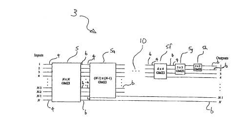
Referring to Figure 2, a generic cascaded configuration of the cascaded N x N
non-blocking optical switch 3 is shown. An N x N GMZI 5 has 1 to (N - 1 )
output ports 6
optically coupled to 1 to (N - 1 ) input ports 4 of an (N - 1 ) x (N - 1 )
GMZI Sa. The
cascaded non-blocking switch is illustrated with a break in structure 10 from
the (N -
1 ) x (N - 1 ) GMZI 5a to a 4 x 4 GMZI Sf. The break in structure 10 after the
(N -
1 ) x (N - 1 ) GMZI Sa is used to indicate that the number of cascaded GMZIs
varies
according to design requirements. The cascaded non-blocking optical switch 3
terminates
with the first three output ports 6 of a 4 x 4 GMZI Sf optically coupled to
three input
ports 4 of a 3 x 3 GMZI Sg, and the first two output ports 6 of a 3 x 3 GMZI
Sg optically
coupled to two input ports of a 2 x 2 GMZI Sh. The N x N GMZI 5 is upstream.
Alternatively, the 2 x 2 GMZI Sh is upstream. Further alternatively, both are
upstream
and downstream when light propagates bi-directionally.
If the N x N GMZI 5 is removed from the N x N non-blocking optical switch 3 an
(N - 1 ) x (N - 1 ) non-blocking optical switch remains. The (N - 1 ) x (N - 1
) non-blocking
optical switch comprises N - 2 GMZI's each having a different number of
waveguide
arms, the number of waveguide arms ranging from 2 to N - 1, where the N - 2
GMZI's are
arranged in descending order by the number of waveguide arms, such that each
GMZI
other than a terminal GMZI with 2 waveguide arms 5h and an initial GMZI with N
- 1
waveguide arms Sa is disposed between two GMZI's - one with one more waveguide
arm
and one with one less waveguide arm - each GMZI having a single free output
port and
each port other than the free output port within a GMZI optically coupled to
one and only
one port of an adj acent GMZI. Of course, it is possible to rearrange the GMZI
order so
long as the available permutations provide for non-blocking operation.
For a desired light routing permutation from the N x N non-blocking optical
switch 3, consider first a beam of light launched into an input port 4 to be
routed to an N
th output port 6, and configure the N x N GMZI 5 such that the beam of light
launched
into input port 4 emerges from the N-th position of the output port 6 of the N
x N GMZI
5. Secondly, consider a beam of light launched into another input port 4 to be
routed to
an (N - 1 )-th output port 6, and configure the (N - 1 ) x (N - 1 ) GMZI Sa
such that light
11
CA 02258333 1999-O1-11
Doc No: 10-105 B CA Patent
from this input port emerges from the (N - 1 )-th position the output port of
the (N -
1 ) x (N - 1 ) GMZI Sa, and so forth. Alternatively, other orderings of the (N
- 2) GMZI's
result in a similar benefit. For example, a 4 x 4, a 2 x 2, and a 3 x 3 a11 in
that order
provide a 4 x 4 non-blocking switch.
In addition, each light routing permutation corresponds to a unique state of
the
optical switch providing an efficient design. Conversely, the number of
possible switch
states is equal to the number of possible light routing permutations, which
ensures that
there is no redundancy in the design. This permits use of a small number of
MMI
couplers, phase shifters, and waveguide crossings to achieve N factorial light
routing
permutations. Specifically, (2N - 2) MMI couplers, (N 2 + N - 2)/2 phase
shifters, and
zero waveguide crossings are required.
Attenuations resulting from paths traversed by optical signals in the cascaded
design are not identical. A signal emerging from the N th output has traversed
two MMI
couplers, while the signal emerging from the (N - 1 )-th output port has
traversed four
MMI couplers, while the signal emerging from the first output port has
traversed a11 (2N -
2) MMI couplers. Since each MMI coupler has a finite excess loss, a signal
emerging
from the N th output port is the least attenuated, while a signal emerging
from the first
output port is the most attenuated. To overcome an imbalance of attenuation,
beams of
light emerging from the output ports are attenuated and/or amplified such that
the beams
of light are of similar intensity.
Balanced Design for Even values of N
Another approach to balancing N x N non-blocking optical switches is by
optically coupling smaller optical switches to each of the input ports 4 and
the output
ports 6 of an N x N GMZI 5. As is evident, additional light routing
permutations
necessary for non-blocking operation are achieved whilst maintaining a
symmetric
balanced design.
12
CA 02258333 1999-O1-11
Doc No: 10-105 B CA Patent
Referring to Figure 3, the basic layout of a balanced 4 x 4 non-blocking
optical
switch 50 is formed from a 4 x 4 GMZI Sf and four 2 x 2 GMZIs Sh. The 4 x 4
GMZI Sf
is constructed in a similar manner as described in Figure 1, in which N = 4.
The 4 x 4
GMZI Sf is shown having four input ports 4 and four output ports 6. The 2 x 2
GMZIs
Sh are also constructed in a similar manner as described in Figure 1, in which
N = 2,
however the 2 x 2 GMZIs Sh only require one waveguide arm 26 to have a phase
shifter
28 in order to function as optical switches. Hence, a 2 x 2 GMZI Sh is capable
of
accessing all of its switch states with only a single phase shifter 28. The
first and second
input ports 4 of the 4 x 4 GMZI are optically coupled to two output ports 6 of
a first 2 x 2
GMZI Sh. The second and third input ports 4 of the 4 x 4 GMZI Sf are optically
coupled
to two output ports 6 of a second 2 x 2 GMZI Sh. The first and second output
ports 6 of
the 4 x 4 GMZI Sf are optically coupled to two input ports 6 of a third 2 x 2
GMZI. The
third and fourth output ports 6 of the 4 x 4 GMZI Sf are optically coupled to
two input
ports 6 of a fourth 2 x 2 GMZI. Preferably, the balanced 4 x 4 non-blocking
switch is
constructed such that no waveguide paths cross.
Three active 2 x 2 GMZIs Sh allow 4~2' = 32 light routing permutations to be
achieved, with redundancy. Therefore, a passive 2 x 2 GMZI may be used in
place of
one of the four 2 x 2 GMZI's. The position of the passive 2 x 2 GMZI may be is
chosen
arbitrarily. The 4 x 4 non-blocking optical switch 50 is balanced, since each
path from an
input port to an output port traverses two 4 x 4 MMIs and four 2 x 2 MMIs.
Also, non-
blocking operation is achieved. Within a resulting 32 light routing
permutations are the
threshold 24 unique light routing permutations required for a 4 x 4 optical
switch to
operate as a non-blocking optical switch. Some of the 32 light routing
permutations are
redundant.
In this design both balanced and non-blocking operation are achieved, but with
the tradeoff that the configuration of the optical switch is more complex. In
the balanced
4 x 4 non-blocking optical switch 50, the 32 possible light routing
permutations are not
unique so in some instances different switch configurations are used to
achieve a given
permutation. Consequently, there are numerous ways to achieve some of the 24
light
13
CA 02258333 1999-O1-11
Doc No: 10-105 B CA Patent
routing permutations required for the balanced 4 x 4 non-blocking optical
switch 50. In
some instances, determination of the GMZI states to achieve a given
permutation are
more complex than for the cascaded design. Of course, when a look up table is
used for
storing the GMZI states, there is no additional complexity.
A set of cross-connects (i, k) for the 4 x 4 GMZI Sf is shown in Table 2. A
configuration state of the GMZI corresponds to a single row. An imaginary
bisection line
(dashed line) drawn in Figure 3 splits the N x N GMZI. This is indicated in
Table 2 by a
dashed line. The set of all possible crossovers of the input ports i from one
side of the
bisection line to the output ports k on the other side is obtained within the
four GMZI
states. Hence, non-blocking operation is possible using a 4 x 4 GMZI Sf. In
Figure 3,
consider an imaginary line that bisects the optical switch symmetrically along
its path.
This line bisects the 4 x 4 GMZI Sf, but does not cross any of the other
components. In
Table 2, this bisection of the 4 x 4 GMZI Sf is represented by shading the
inputs on the
top and bottom portions of the GMZI differently. For non-blocking operation,
the optical
switch must be capable of routing light launched into any possible number of
input ports
from the top half of the optical switch to the same number of output ports
from the
bottom half, and vice-versa. This is because the 4 x 4 GMZI Sf is the only
region in the
optical switch where light launched into input ports within the top half of
the optical
switch is capable of being routed to the bottom half of optical switch, and
vice-versa.
The 2 x 2 GMZIs Sh are confined to routing light within either the top or
bottom half of
the device, and therefore cannot perform this " crossover" function. In this
example, the
4 x 4 GMZI Sf is capable of 0, 1, and 2 crossovers of input signals from the
top half to
output ports in the bottom half, and vice-versa. It is this property of the 4
x 4 GMZI Sf,
which results in non-blocking operation of the 4 x 4 optical switch 50.
To configure the balanced 4 x 4 non-blocking optical switch 50, first consider
the
light routing permutation to determine how many crossovers of the bisection
line are
necessary. Second, set the 4 x 4 GMZI 5f to the corresponding state,
determined from
Table 2. Third, the 2 x 2 GMZIs are each set in either the bar or cross state
to achieve the
desired permutation. In this manner, a control table for the 4 x 4 optical
switch is
14
CA 02258333 1999-O1-11
Doc No: 10-105 B CA Patent
derived. One possible set of control states for the 4 x 4 balanced non-
blocking optical
switch is given in Table 3. The 4 x 4 GMZI state corresponds to the relevant
row in
Table 2, and is abbreviated by the first pair (i, k). In this configuration,
the top left 2 x 2
GMZI is operated in the passive, cross-state, as in Figure 3. The efficiency
of this design
approach, however, is obtained at the expense of driving the fourth 2 x 2 GMZI
switch.
Because only three of the four possible 4 x 4 GMZI Sf states are used, a11
four 2 x 2
GMZIs Sh must now be capable of active operation.
From the above description, it is appreciated that a balanced non-blocking
optical
switch results when a passive 2 x 2 GMZI Sh is replaced by a device that
attenuates light
entering or exiting ports to substantially the sane extent as the passive 2 x
2 GMZI Sh. A
similar attenuation of beam power is found for a beam passing through a
specific
attenuator as that for a beam passing through the 2 x 2 GMZI Sh.
As detailed above, when considering the balanced 4 x 4 non-blocking optical
switch 50 comprising the 4 x 4 GMZI Sf a number of possible configurations
exist. A
first configuration is one in which all four waveguide arms 26 of the 4 x 4
GMZI have a
means for changing their optical length and the 4 x 4 GMZI is optically
coupled to four 2
x 2 GMZIs. Optionally, one of the 2 x 2 GMZIs is passive, i.e., cross-state,
and all
possible switching states are obtainable. Alternatively, one of the 2 x 2
GMZIs has no
means for changing optical path length of connecting waveguide arms 26 between
two
MMIs that make up the 2 x 2 GMZI. In another embodiment one of the 2 x 2 GMZIs
is
replaced by a medium or any device that attenuates a light beam to
substantially the same
degree as a beam passing through the 2 x 2 GMZI.
In a similar manner, the design of balanced non-blocking optical switches is
possible for larger values of N, where N is even. A bisection line is drawn in
the cross-
connect table of the N x N GMZI. The cross-connect capability of the N x N
GMZI
ensures that every possible number of crossovers is achievable within the N
states. The
N x N balanced non-blocking optical switch is formed by connecting the ports
on a given
side of the bisection line to a smaller non-blocking optical switch. In
general, the smaller
CA 02258333 1999-O1-11
Doc No: 10-105 B CA Patent
non-blocking optical switches are operated actively. As an example of a
balanced optical
switch configuration for larger N, referring to Figure 4, the basic layout of
a balanced 8 x
8 non-blocking optical switch 60 is formed from an 8 x 8 GMZI Sj and four 4 x
4 non-
blocking optical switches 50. The 8 x 8 GMZI Sj is constructed in a similar
manner as
described in Figure 1, however, waveguide arms 26 and phase shifters 28 are
not shown.
The 4 x 4 non-blocking optical switches 50 are constructed in a similar manner
as
described in Figure 3. The 8 x 8 GMZI Sj and the four 4 x 4 non-blocking
optical
switches 50 are shown as rectangular boxes with input ports 4 and output ports
6. The
8 x 8 non-blocking optical switch 60 is constructed in a similar manner to the
non-
blocking optical switch described in Figure 3. In Table 4 cross-connects for
the 8 x 8
GMZI Sj are given. Table 4 provides the set of cross-connects (i, k) for the 8
x 8 GMZI
5f in which a given state of the 8 x 8 GMZI corresponds to a single row. The
set of all
possible crossovers about a line that divides the device into two regions
(shown dashed)
is obtained within the eight GMZI states. Hence, non-blocking operation is
possible
using the 8 x 8 GMZI. The input ports and the output ports are bisected as
indicated by
the shading, and the number of crossovers for each state are counted. Since
the ports are
divided into groups of four, it is possible to connect balanced 4 x 4 non-
blocking optical
switches to both sides of the 8 x 8 GMZI to obtain the necessary light routing
permutations for the 8 x 8 balanced non-blocking optical switch.
It is possible to write a software program to determine the GMZI states needed
to
achieve a desired output permutation. Configuration of the GMZIs follows the
procedure
used in the 4 x 4 balanced non-blocking optical switch. The program first
determines
which of the GMZI states yields the number of crossovers indicated by the
desired output
permutation. Once these states are determined, the configuration tables of the
smaller
non-blocking optical switches are used to arrive at the desired permutations.
Optionally,
the software program optimizes the switch to eliminate unnecessary phase
shifters and to
minimise required power for driving the phase shifters where possible. As
mentioned
previously, the configuration states are not unique, and it may be possible to
operate a
number of the smaller component GMZIs in a passive mode.
16
CA 02258333 1999-O1-11
Doc No: 10-105 B CA Patent
From the above described switches, it is evident that by optically coupling
two
GMZIs in series, a greater switching capacity is obtained over an isolated
GMZI.
Numerous other embodiments may be envisaged without departing from the spirit
and
scope of the invention.
17
CA 02258333 1999-O1-11
Doc No: 10-105 B CA Patent
Table 1.
Light Routing 3 x 3 GMZI States
Permutations
1 2 3_
1 3 2 1 3 2
2 1 3 2 1 3
2 3 1
3 1 2
3 2 1 3 2 1
18
CA 02258333 1999-O1-11
Doc No: 10-105 B CA Patent
Table 2.
4 x 4 GMZI Switch State I Crossovers
(1,1) (2,3) (3,2) (4,4) ~ 1
(1',2) (2,1) (3,4) (4,3) ~ 0
(1,3) (2,4) (3,1) (4,2) ~ 2
(1,4) (2,2) (3,3) (4,1) ~ 1
19
CA 02258333 1999-O1-11
Doc No: 10-105 B CA Patent
Table 3.
Light Routing 4 x 4 GMZI State 2 x 2 GMZI States
Permutation
Lower Left ~ Top Right ~ Lower Right
1 2 3 4 (1,2) CROSS BAR $A
1 2 4 3 (1;2) BAR BAR BAR
1 3 2 4 (1,4) CROSS CROSS CROSS
1 3 4 2 (1,4) CROSS CROSS BAR
l 4 2 3 ('1,4) BAR CROSS CROSS
I 4 3 2 (1,4) BAR CROSS BAR
2 I 3 4 (1,2) BAR CROSS CROSS
2 1 4 3 (1,2) CROSS CROSS CROSS
2 3 1 4 (1,1) BAR BAR BAR
2 3 4 1 (1,1) BAR BAR CROSS
2 4 1 3 (1,1) CROSS BAR BAR
2 4 3 1 (1,1) CROSS BAR CROSS
3 1 2 4 (1;4) CROSS BAR CROSS
3 1 4 2 (1,4) CROSS BAR BAR
3 2 1 4 (1,1) BAR CROSS BAR
3 2 4 1 (1,1) BAR CROSS CROSS
3 4 1 2 (1;3) CROSS CROSS CROSS
3 4 2 1 (1,3) CROSS CROSS BAR
4 1 2 3 (1,4) BAR BAR CROSS
4 1 3 2 (1,4) CROSS BAR BAR
4 2 1 3 (1,1) CROSS CROSS BAR
4 2 3 1 (1,1) CROSS CROSS CROSS
4 3 1 2 (1,3) CROSS BAR CROSS
4 3 2 1 (1,3) CROSS BAR BAR
IZ
S
~ ~ ~I'8) ~~'L) ~Z'9) ~S'S) ~~'b) ~L'~) ~9'Z) ~8'T)
b ~Z'8)~i'L)~b'9)~'S) '~9'b)~S') ~8'Z)~G'I)
Z ~'8) ~S'G)~i'9)~L'S)vZ'~b)~8') ~t~'Z)~9'i)
O'8) ~Z'L)Q9'9)~i'S)U8'b)t'E) ~G'Z)~S'i)
i ~S'8)~L'G)C'9)~8'S)ti't~)C9') ~Z'Z)O'I)
Z Q9'8)O'L) Q8'9)~Z'S)EL'~)~I') ~S'Z)~'I)
0 ~G'8)~8'L)~S'9)~9'S)U Ob') O OZ'I)
''b) I'Z)
i Q8'8)~9'G)~G'9)O'S) (S'b)~Z') ~'Z)~i'I)
s.~anosso~~ ~ al~ls uallMs IZL~IJ 8 X 8
'b aI9~,L
~ua~~d H~ 8 SOi-OI ~ol~IaoQ
ii-i0-666l ~~~8SZZ0 ~a