Note: Descriptions are shown in the official language in which they were submitted.
CA 02258360 1999-O1-11
1
TITLE: COUPON MONITOR FOR CATHODIC PROTECTION SYSTEM
BACKGROUND OF THE INVENTION
Field Of The Invention
This invention relates generally to cathodic
protection systems for protecting metal objects, which are
buried in soil, from corrosion. The invention more
particularly relates to a circuit for monitoring electrical
parameters associated with the buried object and a coupon
and reference electrode which are conventionally installed
to provide information about the effectiveness of the
cathodic protection.
Description Of The Related Art
Metal structures such as pipes and tanks, which are
buried in soil, are naturally subjected to an electro
chemical corrosion process in their underground
CA 02258360 1999-O1-11
2
environment. The metal structure acts as an electrode and
the soil an electrolyte so that an electrolytic cell is
formed causing corrosion of the buried structure.
Cathodic protection has commonly been applied to such
S buried objects in order to counteract and thereby mitigate
the electro-chemical corrosion reaction. Such cathodic
protection systems are monitored in order to determine a
level of cathodic protection which is sufficient to
adequately mitigate the corrosion of the buried metal
object. The level considered sufficient is determined by
industry accepted standards, based upon a measurement of
the potential difference between the buried object and a
standard reference electrode also placed in contact with
the soil electrolyte.
IS One problem with measuring this potential arises from
potential differences in the soil resulting from currents
through the distributed resistance of the soil. It is
necessary to turn off the cathodic protection in order to
eliminate the voltage drop arising from the cathodic
protection current flowing through the distributed
resistance of the soil. However, not only does this
interrupt the protection, but it does not eliminate
additional voltage drops in the soil which result from
stray currents from underground power sources, such as
transit systems which cannot be turned off. Additionally,
CA 02258360 1999-O1-11
3
long buried pipelines commonly have a series of several
cathodic protection systems spaced along the pipeline.
Elimination of the IR drop through the soil from the
neighboring cathodic protection systems would require that
a11 cathodic protection systems be turned off during
measurement of the pipe to reference electrode voltage.
In order to avoid these problems, coupons are used to
monitor the level of cathodic protection on buried metal
objects. A coupon is a bare metal electrode having
substantially the same metallurgical, and therefore
electro-chemical, attributes as the buried metal object.
The coupon is buried in the soil near the buried metal
object so that it is subjected to the same corrosive
effects and the same cathodic protection as the buried
metal obj ect . Consequently, the coupon is used to simulate
the buried metal object and potential difference
measurements are taken between the coupon and the reference
electrode. This allows the application of cathodic
protection to the buried metal object to continue
uninterrupted, while only the cathodic protection to the
coupon is interrupted for purposes of taking measurements.
The coupon reference potential therefore simulates the
potential of a coating defect or holiday on the buried
metal object.
In order to evaluate such a cathodic protection system
CA 02258360 1999-O1-11
4
there are three electrical parameters which are commonly
measured. The first is the electrical current between the
coupon and the pipe, the second is the voltage, EoN, between
the pipe and the reference electrode when current is
flowing between the coupon and the pipe, and the third is
the voltage, EpFF, between the coupon and the reference
electrode at some standard time delay after the coupon-pipe
current is interrupted.
These electrical parameters are conventionally
measured by an individual technician travelling into the
field and connecting a strip chart instrument to the
coupon, pipe and reference electrode connections provided
at the site of the coupon and reference electrodes. The
technician connects the instruments, takes readings and
interrupts the electrical connection between the pipe and
the coupon to obtain a measurement of EoFF. The technician
must then examine the strip chart and visually determine
the appropriate values to record.
One difficulty with such manual measurement is that
the values fluctuate with time. The technician must follow
the time line of the strip chart for the time delay of the
standard test utilized by the particular company
responsible for cathodic protection, and estimate the
appropriate EOFF voltage by visual inspection of a
meandering line on a strip chart. This manner of
CA 02258360 1999-O1-11
measurement is not only inherently inaccurate because of
its dependence upon visual inspection and mental
interpolation, but also requires training and skill on the
part of the technician who is going into the field to make
5 the measurements.
It is therefore an object and feature of the invention
to provide a coupon monitor which is capable of making
automated measurements of these corrosion coupon
parameters.
It is a further object and feature of the invention to
allow complex, interrupted potential and current
measurements to be easily detected and recorded in the
field using a simple digital voltmeter giving a direct
reading of the detected potentials and current, so that
these can be reliably recorded by persons who do not
possess as much skill as currently required.
It is a further object and feature of the invention to
provide a coupon monitor which can be attached to a data
acquisition system so that a time sequence of parameters
can be stored, subsequently downloaded, and utilized by a
digital data processing system.
SUN~MARY OF THE INVENTION
The invention is a circuit for monitoring electrical
parameters associated with a buried metal object, a coupon
CA 02258360 1999-O1-11
6
and a reference electrode. A voltage detector circuit is
connected to detect the voltage between the reference
electrode and the coupon and preferably also the voltage
between the reference electrode and the buried object. A
current detector circuit is connected for detecting the
current between the object and the coupon. At least one
sample and hold circuit is connected to the outputs of
these detector circuits for sampling and storing their
measured values of voltage and current. A current
interrupting switch is interposed in series with the
current detector for periodically interrupting the pipe-
coupon current. The interrupter switch, as well as the
sample and hold circuits, are controlled by a controller
circuit. Preferably, there are three sample and hold
circuits, two for sampling and holding the output of the
voltage detector and the other for sampling and holding the
output of the current detector. Additionally, it is
preferred that a low pass filter be interposed between each
detector circuit and the sample and hold circuit connected
to its output, and that the current detector circuit also
be capable of maintaining a substantially zero voltage
between the object and the coupon.
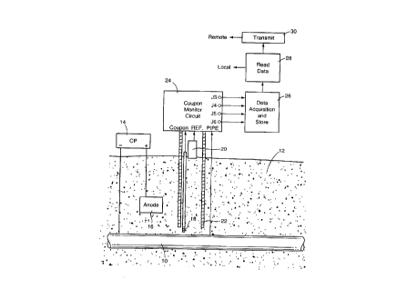
BRIEF DESCRIPTION OF THE DRAWINGS
Fig. 1 is a diagram in vertical section illustrating
CA 02258360 1999-O1-11
7
the connection of the present invention to a cathodically
protected structure, a coupon and a reference electrode.
Fig. 2 is a block diagram illustrating the preferred
embodiment of the invention.
Fig. 3 is a schematic diagram illustrating the details
of the principal circuitry of the preferred embodiment of
the invention.
Figs. 4-10 are schematic diagrams of additional
components of the preferred embodiment of the invention.
In describing the preferred embodiment of the
invention which is illustrated in the drawings, specific
terminology will be resorted to for the sake of clarity.
However, it is not intended that the invention be limited
to the specific terms so selected and it is to be
understood that each specific term includes a11 technical
equivalents which operate in a similar manner to accomplish
a similar purpose. For example, the word connected or
terms similar thereto are often used. They are not limited
to direct connection but include connection through other
circuit elements where such connection is recognized as
being equivalent by those skilled in the art . In addition,
many circuits are illustrated which are of a type which
perform well known operations on electronic signals . Those
skilled in the art will recognize that there are many, and
in the future may be additional, alternative circuits which
CA 02258360 1999-O1-11
8
are recognized as equivalent because they provide the same
operations on the signals.
DESCRIPTION OF THE PREFERRED EMBODIMENT
Fig. 1 illustrates a pipe 10 buried in a soil 12 and
protected by a cathodic protection system, including a DC
power supply 14 electrically connected to the pipe 10 and
to a buried anode 16. For monitoring the level of cathodic
protection, a coupon 18 is buried in the soil 12 near the
pipe 10 and a reference electrode 20 is also positioned in
electrical contact with the soil 12. The coupon 18 and
reference electrode 20 may be of conventional structure, or
may be positioned within a surrounding, non-conductive,
cylindrical tube 22 in accordance with an invention which
is the subject of a separate patent application.
The present invention is a coupon monitor circuit 24
electrically connected to the pipe 10, the coupon 18, and
the reference electrode 20 at suitable input terminals.
Output data from the coupon monitor circuit 24 appears at
output terminals J3, J4, and J5, referenced to ground
terminal J6, in the form of DC voltage levels representing,
and preferably proportional to, the pipe-coupon current,
the pipe/reference voltage, EoN, and the coupon/reference
voltage, EpFF, measured a predetermined time interval after
the pipe-coupon current is interrupted.
CA 02258360 1999-O1-11
9
This output data may be read by simply applying one
probe of a digital multimeter or voltmeter to output
terminal J6 and the other probe sequentially in turn to
terminals J3, J4, and J5. Alternatively, however, these
S output data may be applied to a conventional data
acquisition and storage device 26 where they may be stored
for later transfer through a data reading circuit 28 for
local readings and/or to a transmitter 30 for wire line or
wireless transmission to an area remote from the coupon
monitor circuit 24.
Fig. 2 is a block diagram illustrating the basic
components of the coupon monitoring circuit of the present
invention. The voltage detector circuit 32 has its voltage
detecting input connected between the terminal 34, which is
connected to the reference electrode 20, and the terminal
36, which is connected to the coupon 18. The output of the
voltage detector circuit 32 is applied to sample and hold
circuits 38 and 50, which are capable of sampling and
storing the output of the voltage detector circuit 32.
This output voltage represents the coupon/reference
voltage.
The monitoring circuit also has a zero resistance
current detector circuit 40 series connected to a current
interrupter switch 42. The series current detector circuit
40 and interrupter switch 42 are connected between the
CA 02258360 1999-O1-11
coupon terminal 36 and the terminal 44 connected to the
pipe. A single pole, triple throw, mode switch 46 is
interposed in the series connection between the pipe
terminal 44 and the coupon terminal 36. It is positioned
5 at position 1 for normal monitoring operation. Position 2
represents an inoperative state of the coupon monitoring
circuit which maintains the pipe-coupon connection and
cathodic protection of the coupon. In position 2 the pipe
and coupon are maintained at the same potential by
10 conduction through the circuit. In position 3, both the
monitoring circuit and cathodic protection of the coupon
are inactive. Position 3 is utilized, for example, after
installing a new coupon because it is desirable that the
coupon become settled and tightly surrounded by the soil in
the same manner as the pipe. Furthermore, a new coupon
will generally have a clean, uncorroded surface, and
consequently will be electro-chemically different than a
previously installed pipe, even though the metals are
identical. Therefore, connecting a newly installed coupon
to an older pipe may cause galvanic action or other
problems. As a result, the mode switch is switched to
position 3, while the coupon settles for a period of time
on the order of a month or two before being switched to
position 1 or 2.
A sample and hold circuit 48 is also connected to the
CA 02258360 1999-O1-11
11
output of the current detector circuit 40 for sampling and
storing the output of the current detector circuit 40. The
current interrupter switch 42 periodically interrupts the
current through the current detecting circuit 40 to permit
measurement of the couponJreference voltage, EopF, a
selected time period after the current interrupter switch
42 is opened to prevent current flow through the zero
resistance current detector circuit 40.
A third sample and hold circuit 50 is also connected
to the output of the voltage detector 32. Three sample and
hold circuits are used to assure that a11 outputs (EoN, EOFF
and I) are available at a11 times. It should be apparent
to those skilled in the art that a separate and additional
voltage detector circuit could be connected between the
reference electrode terminal 34 and the pipe terminal 44
for detecting the pipe/reference voltage, EoN, and it could
be connected to the sample and hold circuit 50. However,
instead the circuit may be simplified and the additional
voltage detector circuit avoided by recognizing that, when
the interrupter switch 42 is closed to permit current flow
through the zero resistance current detector circuit 40,
the pipe terminal 44 is essentially short circuited to the
coupon 36 and consequently the voltage appearing at the
input to the voltage detector circuit 32 in this state is
the pipe/reference voltage. However, when the current
CA 02258360 1999-O1-11
12
through the zero resistance current detector circuit 40 is
interrupted by interrupter switch 42, then the input to the
voltage detector circuit 32 is the coupon/reference
voltage, E~pp. This permits the single voltage detector 32
to be used with two separate sample and hold circuits 38
and 50 for respectively sampling both EoFF and EoN.
A microprocessor controller 51, illustrated in more
detail in Fig. 10, is crystal controlled and has outputs
connected to the sample and hold circuits 38, 48, 50 and 42
l0 for switching them between their sampling state and holding
state and controlling timing of current interruption.
The details of the preferred circuitry are illustrated
in Figs. 3-10 with specific component identification shown
in Table 2. Referring to Fig. 3, the voltage detector 32
has a differential amplifier U4 and is connected through a
low pass, active filter circuit 52 to the sample and hold
circuit 50. Similarly, the output at pin 6 of the voltage
detector circuit 32 is also applied through a low pass,
active filter 54 to the sample and hold circuit 38. The
mode selection switch 46 is connected from the coupon
terminal 36 through the interrupter switch 42 and through
the current detector circuit 40 to the pipe. The output
from the current detector circuit 40 is similarly applied
through a low pass filter 56 to the sample and hold circuit
48. Each of the low pass filter circuits 52, 54 and 56 is
CA 02258360 1999-O1-11
13
an analog active filter having a pass band with a cut off
at substantially lOHz. The pass band could also extend
alternatively to other similar low frequencies, such as 5Hz
or lHz. The low pass filter eliminates the effects of
periodic AC variations generated by the cathodic protection
system and stray currents.
The current interrupter switch 42 comprises three pi-
configured switches. These switches are a bridging switch
U5b and switches U5a and U5c which are legs of the pi
configured switches. The current detector circuit 40
includes an op amp Ulb having its non-inverting input
connected through common and ground to the pipe terminal 44
and its inverting input connected through the interrupter
switch 42 and the mode selector switch 46 to the coupon
terminal 36. The op amp Ulb provides a high input
impedance first amplifier stage having an output driving a
second power amplifier stage 58, comprising transistors Q1
and Q2. The current output of the power amplifier 58 flows
through a current sensing resistor R1 so that the output
current of the power amplifier 58 flows through both R1 and
switch U5b to the coupon terminal 36.
Therefore, the voltage difference between the coupon
and pipe is applied to the inputs of the operational
amplifier Ulb. A continuous current path exist from the
coupon through switch USb, resistor R1, the power amplifier
CA 02258360 1999-O1-11
14
circuit 58, and the power supply for the power amplifier
circuit 58 to the pipe. That power supply is illustrated
in Fig. 4, and its filter capacitors are illustrated in
Fig. 5. As known to those skilled in the art, the
operational amplifier Ulb has a very high gain and has
essentially zero voltage difference between its inverting
and non-inverting inputs. Consequently, the current
detecting circuit 40, when connected by interrupting switch
42 between the coupon and the pipe, operates as a negative
feedback control system in which the power amplifier 58 and
its power supply drive sufficient current between the
coupon and pipe to maintain the pipe/coupon voltage, which
is applied to the inputs to differential amplifier Ulb, at
essentially zero volts. Since the coupon/pipe voltage is
maintained at zero regardless of the current through it,
the current detector circuit 40 provides an apparent zero
resistance short circuit between the coupon and pipe, with
the current through R1 being the coupon-pipe current. The
voltage across the resistor R1 is directly proportional to
the coupon-pipe current through resistor R1. That voltage
is applied through differential amplifier U6 to the low
pass filter 56 and the sample and hold circuit 48 to
represent the coupon-pipe current.
Three sample and hold switches, U3a, U3b, and U3d, as
well as the three switches USa, USb, and USc, forming the
CA 02258360 1999-O1-11
interrupter switch 42, are each connected to the micro
controller 51 illustrated in Fig. 10. The micro controller
cycles the states of these six switches through a sequence
of six states which are periodically repeated and are
5 illustrated in Table 1.
Amplifiers U2a, U2b, and U2c, which form a part of the
sample and hold circuits 38, 48 and 50, are impedance
transforming or isolating amplifiers providing a DC output
at output jacks J3, J4, and J5, which is proportional to
10 the voltages of capacitors C9, C10, and C11 at their inputs
without draining any significant charge from those
capacitors. The op amps U2a, U2b, and U2c, are selected to
have an ultra-low droop rate preferably on the order of 0.1
millivolt per second. This prevents any significant
15 discharge of the voltage level maintained on capacitors C9,
C10, and C11 as a sample, despite the use of very low
update frequencies, typically substantially less than
O.lHz.
Turning to the operation of the embodiment illustrated
in Figs. 3-10, Table 1 is a truth table showing the states
of these six switches.
CA 02258360 1999-O1-11
16
TABLE 1
State T~3_aU3b U3d U5a U5b U5c
and
Time
(0 is open,C close d)
is
1. Equilibrium 0 O O O C C
Seconds
10 2. Sample EoN and C 0 C O C C
Pipe-Coupon Current
100 milliseconds
3. Hold Samples 0 0 0 O C C
At End of State 2
100 milliseconds
4. Interrupt Pipe-Coupon 0 O O C O 0
Current
100 milliseconds
5. Sample EoFF 0 C O C 0 O
(current interrupted)
100 milliseconds
6. Hold EoFF Value 0 O O C O O
At End Of State 5
(current interrupted)
0.5-1 second
Return
to
State
1.
In state 1, switches U5b and U5c are closed and
consequently current flows through resistor R1 between the
coupon and the pipe. State 1 continues for a time interval
which is considerably longer than the other states and is
typically 10 seconds so that the entire system comes into
equilibrium and the coupon is maintained in the same
electrical state as the pipe for a time period which is
CA 02258360 1999-O1-11
17
considerably longer than the time period during which
measurements are taken. This assures that the measurement
intervals are considerably shorter than the time intervals
of state 1 so that the measurements will not themselves
cause the coupon to experience different conditions than
the pipe and thereby introduce an error into the
measurements. During the interval of state 1, no
measurements are taken.
The microprocessor control then switches to state 2 by
closing the sample and hold switches U3a and U3d. State 2
provides an updated sample of the pipe/reference voltage,
EoN, and the coupon-pipe current I. State 2 is maintained
for an interval, of, for example, 100 milliseconds to allow
the capacitors C10 and C11 to charge through the coupling
resistors R12 and R10. The coupling resistors R10 and R12
are chosen to have a value which is an engineering
compromise to provide a sufficiently high resistance which
prevents generation of a current surge or spike when the
switches U3 are closed, but a sufficiently small resistance
to permit the capacitors C9-C11 to charge fully within the
time interval of state 2 or state 5.
The micro controller then switches the circuit to
state 3 by opening switches U3a and U3d. This holds the
samples taken in state 2, resulting in the application of
continuous DC level output voltages at output jacks ,T3 and
CA 02258360 1999-O1-11
18
J5 during a11 subsequent states, representing EoN and I.
In the preferred embodiment, state 3 also lasts for
substantially 1o0 milliseconds.
The micro controller then switches to state 4 in which
switches U5b and U5c are opened and switch U5a is closed.
State 4 consequently interrupts the coupon-pipe current.
Switch U5a is closed in order to provide feedback to the op
amp Ulb to maintain its stability so that it does not
oscillate. No measurement is taken in state 4. However,
the duration of state 4, which in the preferred embodiment
is 100 milliseconds, provides a portion of the time delay
from the interruption of the current to the measurement of
the coupon/reference voltage, EoFF, commonly referred to as
"instant OFF"
The micro controller then switches to state 5 in which
the switch U3b is closed to initiate sampling of the
reference/coupon voltage, EoFF, under the continued
condition of interrupted current. In the preferred
embodiment, state 5 continues for 100 milliseconds and then
the micro controller switches the circuit to state 6.
In state 6, switch U3b is opened so that the voltage
on capacitor C9 is then held and represents EoFF. State 6
continues for a total of preferably 0.5 to 1 second. The
reason for this time delay is to provide a check during
testing, to allow manual readings if desired and to allow
CA 02258360 1999-O1-11
19
adjustable interruption period timing.
After the time interval of state 6, the micro
controller 51 then returns the circuit to state 1, and the
cycle is periodically repeated.
The sum total of the time durations of states 4 and 5
represents the time interval from current interruption to
the measurement Of FrOFp. It is desirable that the micro
controller be programmable, such as by appropriate jumpers,
so that this total time interval can be programmably
l0 selected. This allows each user to select the user's
preferred time delay following current interruption until
EQpg is measured. For example, the microcontroller circuit
is desirably configured to permit selection of a total
delay of 100, 200, 300, 400, or 500 milliseconds after the
initiation of state 4.
The reason for the pi configuration of the interrupter
switch 42 arises from the fact that the switches U5, like
the switches U3 , are a11 CMOS analog switches controlled by
the micro controller 51. If they had zero resistance, then
switch U5c would be unnecessary. However, CMOS analog
switches typically have a resistance when closed of
approximately 50 ohms. Consequently, if switch U5c were
omitted, the voltage applied to the input of differential
amplifier Ulb, the voltage which the circuit maintains at
essentially zero, would not be the coupon/pipe voltage, but
CA 02258360 1999-O1-11
2Q
would be offset from that voltage by the IR drop through
switch USb, caused by the significant pipe/coupon current.
Therefore, switch USc, which carries essentially no
current, assures that the coupon voltage itself is
accurately input to the differential amplifier Ulb.
As a result of the operation of the circuit of the
present invention, the DC voltages maintained at output
j acks J3 , J4 , and J5 continuously represent EoN, EQFF, and I ,
and these values are updated periodically, for example
every 11-12 seconds. Because these are simple DC values,
they may be read using a digital multimeter. This permits
an untrained person to connect the multimeter probes
between grounded terminal J6, and in turn each of the
terminals J3, J4, and J5, and to simply read a number from
the digital multimeter and manually record the number.
Alternatively, or additionally, the DC output levels at the
jacks can be recorded by a data acquisition and storage
system, or data logger, in sequential, selected intervals
over a substantial period of time. These data can then be
periodically, locally read or transmitted to a remote
location.
CA 02258360 1999-O1-11
21
TABLE 2
Part Description Value
C1, C3, C6, C9, Polypropylene X7R luf
C10, C11 Capacitor
C2, C4, C5 Polypropylene X7R .47uf
Capacitor
C7, C8, C18, C19 Tantalum Capacitor .luf
C12, C13 Ceramic Disc Capacitor l2pf
C14, C15, C16, C1? Tantalum Capacitor 4.7uf
R1, R4, R7 1% Precision 1/4 44K
Watt Resistor
R2, R3, R5, R6, 1% Precision 1/4 22.1K
R8, R9 Watt Resistor
R10, R11, R12 5% 1/4 Watt Resistor 330ohm
UO Dual Charge Pump Max680
Voltage Converter
U1, U2 4 Picoampere Input AD704
Current Bipolar Op
~P
U3, U5 Monolithic Quad SPDT DG412
CMOS Analog Switch
U4, U6 Low Power AD620AN
Instrumental Amplifier
U7 Programmable Micro Pic16C56
Controller
Q1 NPN Transistor PN2222A
Q2 PNP Transistor PN2907A
Z1 Crystal Oscillator 32.768Khz
CA 02258360 1999-O1-11
22
Table 2 coat.
ar escrigt~on Value
Rnl, Rn2 Resistor Array 10K
J1 8 Pin Jumper Jumper
Q3 4 Volt Low Dropout 711 Reg
Regulator
CA 02258360 1999-O1-11
23
while certain preferred embodiments of the present
invention have been disclosed in detail, it is to be
understood that various modifications may be adopted
without departing from the spirit of the invention or scope
of the following claims.