Note: Descriptions are shown in the official language in which they were submitted.
~ s ~
CA 022~8~40 l998-l2-l6
.; -.
WO 97/49271 PCT/DE97/01234
~L~ E13SAM~NDE~
Description ~ i,'A~LATE~N
Mounting rack for plug-in electrical printed
circuit board assemblies having means for damped
dissipation of electrostatic potentials.
A problem which can occur when inserting an
electrical printed circuit board assembly into a
mounting rack is that external electrostatic voltages
and static voltage potentials can cause interference in
the interior of the mounting rack and, in this case, in
particular in the case of other printed circuit board
assemblies which have already been inserted. In this
case, during the insertion process, an electrostatic
voltage is transferred, in particular from a person,
first of all to an electrically conductive, in
particular metallic front panel of the printed circuit
board assembly to be inserted. As a rule, the
electrostatic voltages are very high and, as a result
of discharge processes, for example as a result of
radio-frequency signals produced by a spark gap or as a
result of a rise in potential, can cause interference
with electrical components on the printed circuit board
assembly itself, or on adjacent printed circuit board
assemblies. This is particularly undesirable if it is
intended to be possible to insert and withdraw printed
circuit board assemblies during operation of other
printed circuit board assemblies in the mounting rack.
The insertion and withdrawal of a printed circuit board
assembly during operation of the other printed circuit
board assemblies is called "live insertionn.
Figure la shows a detail of a side section
through the lower region of one known configuration of
a mounting rack BGT. In this case, a detail is once
again illustrated, by way of example, of an electrical
printed circuit board assembly BG. This has at least
one printed circuit board LP, to the front face of
which an electrically conductive, in particular
metallic, front panel FP is fitted, and to the rear
face of which a plug connector V2 is fitted.
CA 02258540 1998-12-16
- wo 97/49271 - la - PCT/DE97/01234
Furthermore, there is a strip sliding contact K which
extends along the lower edge region of the printed
CA 022~8~40 1998-12-16
., .
WO 97/49271 - 2 - PCT/DE97/01234
circuit board LP. This sliding contact K is
electrically conductively connected to the front panel
FP of the printed circuit board assembly BG. At least
one lower guide rail LS is provided on the mounting
rack BGT for insertion of the printed circuit board
assembly BG in the insertion direction ER, and is
fitted between a front and a rear transverse rail QV,
QH. At least one contact spring element F1 is arranged
in the front region in the interior of the mounting
rack BGT and is electrically conductively connected to
it, preferably via the front transverse rail QV located
underneath. The contact spring element is
advantageously integrated in the guide rail. One
possible embodiment for such integration can be found
in German Patent Specification DE 3 24 883 C2. When the
printed circuit board assembly BG is being inserted,
the contact spring element F1 makes contact with the
sliding contact K at the start of the insertion
process, so that an electrically conductive connection
is produced between the front panel FP and the mounting
rack BGT, which is normally at zero voltage potential.
It is disadvantageous that possible external
electrostatic voltages stored on the front panel FP can
produce a spark gap in the interior of the mounting
rack BGT when contact is made between the sliding
contact K and the contact spring element F1 during
insertion of the printed circuit board assembly BG into
the mounting rack BGT. Such a spark gap produces radio-
frequency interference signals which, for example, can
interfere with the operation o~ adjacent printed
circuit board assemblies which have already been
inserted into the mounting rack BGT.
Figure lb shows the mounting rack BGT, which
has already been illustrated in Figure la, with the
printed circuit board assembly BG in the inserted
state. The plug connector V2 on the rear face of the
printed circuit board assembly BG is now inserted into
a corresponding plug connector V1 such that contact is
made, which plug connector V1 is preferably fitted on a
CA 02258540 l998-l2-l6
., ~
- WO 97/49271 - 2a - PCT/DE97/01234
so-called mother board
CA 022~8~40 1998-12-16
, . .
- WO 97/49271 - 3 - PCT/DE97/01234
in the interior of the mounting rack. Potentials which
are applied to the front panel FP from the outside, for
example an electrostatic voltage applied by touching,
flow via the sliding contact K, the contact spring
element F1 and the transverse rail QV to the mounting
rack BGT, which is normally grounded. A problem is
caused by interference which in this case can possibly
be "emitted" via the "antenna-liken strip sliding
contact K deeply into the interior of the mounting rack
lO BGT, and can thus likewise interfere with the operation
of printed circuit board assemblies in the mounting
rack BGT.
Finally, as a rule, at least one contact screw
SR is fitted at the lower end of the front panel FP.
Once the printed circuit board assembly BG has been
completely inserted, this contact screw SR is screwed,
for example, to the lower transverse rail QV and then
acts as a protective contact, which has an adequate
current carrying capacity.
The object of the invention is to dissipate
electrostatic charges on printed circuit board
assemblies to the mounting rack in such a manner that
interference-free operation is ensured of other printed
circuit board assemblies which have already been
inserted into the mounting rack and are in operation.
The object is achieved by the mounting rack
specified in claim 1. Other, advantageous embodiments
are contained in the dependent claims.
An advantage of the mounting rack according to
the invention is that electrostatic charges which are
applied to the front panel can be dissipated to the
mounting rack, damped by an electrical resistor, not in
the manner of a short circuit and with a definable time
constant. As in the case of a resistor/capacitor
circuit, electrical charges are dissipated from the
front panel of the printed circuit board assembly,
which acts as a capacitor, damped via the resistor. The
CA 022~8~40 l998-l2-l6
WO 97/49271 - 4 - PCT/DE97/01234
invention thus prevents sparks from being formed
between the sliding contact and the contact spring
element while the printed circuit board assembly is
- being inserted into the mounting rack. In consequence,
there is advantageously no need to be concerned about
interference signals caused by flashovers in the
mounting rack.
Further spring elements which may also be
present in the interior of the mounting rack represent
a further advantage in one embodiment. As a result of
this, according to the invention, a sliding contact on
the printed circuit board assembly can also make
contact with the mounting rack in the rear region of
the latter. The possible "antenna effect" of the
sliding contact is thus also prevented if interference
is applied from the outside to the front panel when the
printed circuit board assembly is in the inserted
state.
Further advantageous embodiments of the
invention are specified in the corresponding dependent
claims.
The invention will be described in more detail
below with reference to an exemplary embodiment that is
illustrated in the figures, which are described briefly
below and in which:
FIG la shows, by way of example, a side view of the
already explained embodiment of a known
mounting rack,
FIG lb shows, by way of example, the side view of the
already explained, known mounting rack
illustrated in Figure la, with a printed
circuit board assembly completely inserted,
FIG 2a shows the side view of an exemplary embodiment
of a mounting rack according to the invention,
having a resistor between the sliding contact
and the front panel of a printed circuit board
assembly,
CA 022~8~40 1998-12-16
. . .
~ WO 97/49271 - 5 - PCT/DE97/01234
FIG 2b shows the side view of the mounting rack shown
in Figure 2a, with a printed circuit board
assembly completely inserted,
FIB 3a shows the side view of a further embodiment of
the mounting rack according to the invention,
with an additional contact pin on the inside of
the front panel, and
FIG 3b shows the side view of the mounting rack shown
in Figure 3a, with a printed circuit board
assembly completely inserted.
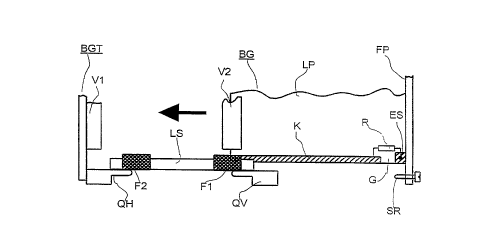
By way of example, Figure 2a shows a side view
of a mounting rack BGT according to the invention, with
an electrical printed circuit board assembly BG which
can be pushed into it. This printed circuit board
assembly BG has an electrically conductive, preferably
metallic, front panel FP and a printed circuit board
LP. At least one lower guide rail LS is advantageously
fitted in the mounting rack BGT in order to allow the
printed circuit board assembly BG to be inserted into
it, and is used to hold and guide the printed circuit
board LP over its edge. An electromagnetically
shielding front face of the mounting rack BGT is formed
in particular by means of the respective front panels
FP of a plurality of printed circuit board assemblies
BG which can be inserted into the mounting rack BGT
alongside one another. On the edge regions, the printed
circuit board LP has at least one strip sliding contact
K with which an electrically conductive contact is
made, during insertion of the printed circuit board
assembly BG, by a means Fl for making electrical
contact between the sliding contact K and the mounting
rack BGT.
According to the invention, the sliding contact
K of the printed circuit board assembly BG is not
directly electrically connected to the front panel FP.
Instead of this, there is an isolation gap G between
the front panel FP and the sliding contact K, which gap
CA 022~8~40 1998-12-16
.. ..
- WO 97/49271 - 6 - PCT/DE97/01234
is bridged by an electrical resistor R which can be
selected. For example, electrostatic charges applied by
a person making touching contact with the front panel
FP are thus dissipated, during insertion of the printed
circuit board assembly BG, virtually without causing
any interference signals at all, by means of a
discharge (which is damped via the resistor) to the
mounting rack BGT, which is normally at ground
potential. The resistor is advantageously connected to
an electrically conductive end piece ES, which is used
to attach the front panel FP to the printed circuit
board LP.
The discharge process in the mounting rack BGT
during insertion of the printed circuit board assembly
BG takes place via the resistor R, the contact strip K
and the means F1 for making electrical contact with the
sliding contact K. This has, in particular, a contact
spring element F1 for making electrical contact with
the sliding contact K and can, for example, be fitted
in the region of the guide rail LS, and/or can be
integrated in it. As soon as the process of inserting
the printed circuit board assembly BG into the mounting
rack BGT starts, the sliding contact K, which is in
general mounted on the printed circuit board LP in the
form of a conductor track, is gripped in a sprung
manner, and made contact with, by the contact spring
element F1.
According to a further embodiment of the
mounting rack BGT according to the invention, this
mounting rack BGT has at least one ~urther means F2 for
making electrical contact between the sliding contact K
and the mounting rack BGT. The means F2 preferably has
a contact spring element F2 for making electrical
contact with the slidlng contact K, which is
electrically conductively connected to the mounting
rack BGT, preferably in the region of the guide rail LS
in the rear region in the interior of the mounting rack
BGT, and corresponds to the contact spring element F1.
Thus, according to the invention, when the printed
CA 02258540 l998-l2-l6
- WO 97/49271 - 6a - PCT/DE97/01234
circuit board assembly BG is being inserted into the
mounting rack BGT, there is also an electrically
CA 022~8~40 1998-12-16
. . .
WO 97/49271 - 7 - PCT/DE97/01234
conductive connection for the strip sliding contact K
in the rear region of the interior of the mounting rack
BGT. The term rear region in this context means that
region of the mounting rack BGT which faces away from
the front panel FP when the printed circuit board
assembly BG is inserted.
The additional contact, according to the
invention, of the sliding contact K in the rear region
of the mounting rack BGT has, in particular, the
advantage that, when the printed circuit board assembly
BG is in the inserted state as is illustrated in Figure
lb, electrostatic charges applied from the outside to
the front panel, in particular, cannot penetrate deeply
into the mounting rack BGT via the strip sliding
contact K. Since the sliding contact K makes contact
with the mounting rack BGT at least on both sides by
means of the contact spring elements F1 and F2, there
are advantageously no long exposed "antenna-liken
regions of the strip sliding contact K. Thus, according
to the invention, possible radio-frequency "emissions"
of interference signals via the sliding contact K are
prevented. The contact spring elements Fl and F2 can be
electrically conductively connected to the mounting
rack BGT in particular by means of a connection to a
~ront and a rear transverse rail QV and QH,
respectively, of the mounting rack BGT.
In a further embodiment of the mounting rack
BGT according to the invention, means are additionally
provided for making electrically conductive contact
between the front panel FP and the mounting rack BGT.
These means are represented by the reference symbol SR
in the figures, and are preferably in the form of a
screw. These means come into play when the front panel
FP is in the inserted state.
Figure 2b shows the mounting rack BGT already
illustrated in Figure 2a, with an inserted printed
circuit board assembly BG and with at least one screw
SR passing through the front panel FP as the means ~or
producing the electrically conductive contact between
CA 02258540 1998-12-16
- WO 97/49271 - 7a - PCT/DE97/01234
the ~ront panel FP and the mounting rack BGT. At least
CA 022~8~40 1998-12-16
- WO 97/49271 - 8a - PCT/DE97/01234
one screw SR in each case preferably passes through the
front panel FP at opposite ends (not illustrated), by
means of which the printed circuit board assembly BG is
screwed to the mounting rack BGT, in particular to a
front transverse rail QV, in the inserted state, such
that electrical contact is made. Thus, according to the
invention, a further contact is made between the
metallic front panel FP and the mounting rack BGT. In
the completely inserted state, this advantageously
results in the capability to discharge electrostatic
charges applied from the outside to the front panel FP,
via the screw SR, directly to the mounting rack BGT, so
that such charges do not reach the interior of the
mounting rack BGT via the contact strip K. Such a
contact means SR, which is preferably like a screw,
bridges the series circuits formed by the resistor R,
the sliding contact K and the electrical contact means
Fl, F2 to the mounting rack BGT.
Figure 3a shows a further embodiment of the
mounting rack BGT according to the invention, in which
case the front panel FP has at least one additional
contact pin KS. This is preferably fitted at the lower
end of the front panel and points into the interior of
the mounting rack, in the insertion direction ER of the
printed circuit board assembly. During the process of
inserting the printed circuit board assembly BG, the
contact pin KS on the front panel FP makes direct
electrically conductive contact with the mounting rack
BGT, via a further contact spring element F4. The
contact spring element F4 is preferably conductively
connected to the lower transverse rail QV.
Such an embodiment according to the invention
is particularly advantageous in the case of printed
circuit board assemblies BG which cannot be screwed to
the mounting rack BGT but, for example, can be latched
to the mounting rack BGT by means of a so-called lever
pulling handle H. In such a case, both the contact pin
KS and the contact spring element F4 are designed to be
suf~iciently mechanically robust that a plurality of
CA 022~8~40 1998-12-16
~ , , .
- WO 97/49271 - 9 - PCT/DE97/01234
~unctions can be carried out at the same time. On the
one hand, the contact pin and contact spring can act as
a mechanical guide ~or the printed circuit board
assembly during the insertion process, so that it is
possible to prevent the printed circuit board assembly
~rom being displaced laterally. Furthermore, when the
printed circuit board assembly is in the completely
inserted state, the two elements can be used as a so-
called protective contact. This facilitates a ground
connection ~or the ~ront panel, in accordance with the
VDE requirements. It is then possible to dispense with
an additional screw SR, as is illustrated according to
the prior art in Figures la and lb. Finally, the two
elements can also produce a mechanical joint between
the printed circuit board assembly and the mounting
rack such that there is no longer any need ~or an
additional screw ~or ~urther ~ixing.
The contact spring element F4 is in this case
preferably ~itted in the ~ront region o~ the mounting
rack BGT, in the region o~ the guide rail LS, and is
electrically conductively connected to the mounting
rack BGT. The contact spring element F4 may be
electrically conductively connected to, for example, a
front transverse rail QV o~ the mounting rack BGT.
When the printed circuit board assembly BG is
being inserted, the contact pin KS makes electrically
conductive contact with the contact spring element F4
be~ore the connection is made between the plug
connector V1 of the mounting rack BGT and the plug
connector V2 o~ the printed circuit board LP of the
printed circuit board assembly BG. Thus, in addition to
the sliding contact, there is a ~urther option ~or
advantageously discharging electrostatic charges
located on the ~ront panel FP via the contact pin KS
and the contact spring element F4 to the mounting rack
BGT be~ore the assembly BG is brought into use by the
mating o~ the plug connectors V1 and V2.
Figure 3b shows the mounting rack BGT already
illustrated in Figure 3a, with an inserted printed
CA 02258540 1998-12-16
~, .
- WO 97/49271 - 9a - PCT/DE97/01234
circuit board assembly BG. According to the invention,
when the printed
CA 022~8~40 l998-l2-l6
WO 97/49271 - lO - PCT/DE97/01234
circuit board assembly BG is in the inserted state,
electrostatic charges applied in particular from the
outside to the front panel FP can advantageously be
discharged via the contact pin KS and the contact
spring element F4 directly to the mounting rack BGT,
and do not pass via the contact strip K into the
interior of said mounting rack BGT.
An advantage of a mounting rack according to
the invention is, in particular, the capability to
insert and withdraw a printed circuit board assembly BG
even during operation of the other, further printed
circuit board assemblies in the mounting rack without
this causing any emission of interference signals which
could adversely affect the correct operation of the
other printed circuit board assemblies in the mounting
rack BGT.