Note: Descriptions are shown in the official language in which they were submitted.
CA 02258673 2004-03-04
WO 98/02830 PCT/US97/13201
- 1-
LOW POWER PARALLEL CORRELATOR FOR
MEASURING CORRELATION BETWEEN
DIGITAL SIGNAL SEGMENTS
BACKGROUND OF THE INVENTION
Field of the Invention
This invention generally relates to spread spectrum
communications systems and, more particularly, to a low-power signal
processing architecture and method for spread spectrum receivers.
Background Description
Spread spectrum communication is advantageous in
communication applications requiring high reliability in a noisy
environment. Often the dominant noise is man-made interference,
either intentional or accidental. In a specific application the
communication environment may include many potential reflectors,
giving rise to severe multi-path interference. Such multi-path
interference typically insinuates deep nulls in the form of frequency
CA 02258673 1998-12-17
WO 98/02830 PCT/US97/13201
-2-
selective fading. Spread spectrum communications is an excellent
countermeasure to these difficulties.
There are several types of spread spectrum systems including
direct sequence spread spectrum systems, frequency hopping systems,
s time hopping systems, pulse frequency modulated (or chirp) systems,
and various hybrids. Of these, the direct sequence spread spectrum
(DSSS) systems and frequency hopping systems are perhaps the more
widely implemented. The following discussion is focused on binary
DSSS systems.
~o In binary DSSS communication, a wide band carrier signal is
modulated by a narrow band message signal. The wide-band carrier is
typically generated by bi-phase modulating a single frequency carrier
using a binary pseudo-random noise (P/N) code sequence. The P/N
code is often generated using one or more high speed shift registers,
is each having modulo-two feedback according to a primitive polynomial.
The generated high-speed PIN code is then applied to a balanced
modulator (multiplier) whose other input signal is the narrow band
carrier. The output signal of the balanced modulator is a wide-band
signal often referred to as a "wide-band carrier". To communicate data,
2o the wide-band carrier is bi-phase modulated by a binary message data
stream. The message data rate is usually much lower than the
P/N-code symbol or "chip" rate, and the data and code-chip edges are
usually synchronized. The ability of the DSSS technique to suppress
interference is directly proportional to the ratio of the code-chip rate to
zs the data rate. In many applications, there are thousands of code chips
per message bit.
A DSSS signal can be received by first shifting the signal down
to baseband by multiplying it with a locally generated replica of the
original narrow-band carrier {e.g., a properly tuned local oscillator). If
3o the frequency (and phase) of the carrier replica is the same as that of
the received original narrow-band carrier, then the multiplier output
signal will be a bipolar "wide-band data" stream that is the product of
the bipolar P/N code and message-data sequences. The P/N code is
SUBST'(TUTE SHEET (RULE 26)
CA 02258673 1998-12-17
WO 98/02830 PCT/US97/13201
-3-
then removed by multiplying the wide-band data stream with a locally
generated replica of the P/N code that is time aligned with the received
PIN code. This is the data de-spreading process and yields the original
message data stream at the multiplier output.
s In the data de-spreading process, the wide-band data power
spectrum is refocused into the original narrower data bandwidth, raising
the data power level well above the background noise in that
bandwidth. The amount that the power level is raised is the so called
processing gain and is directly proportional to the ratio of the code rate
Io to the data rate. Furthermore, any received narrow-band interference is
spread by the code-replica modulation, and this greatly reduces the
interference power level in the data band.
An often difficult task associated with DSSS signal reception is
that of generating the carrier replica with bath proper carrier frequency
is and phase and generating the P/N code replica at the proper rate and
with proper time alignment (offset). In many DSSS communication
systems, the necessary carrier frequency, carrier phase, and P/N code
offset are not known a priori at the receiver and these parameters must
be determined by trying different values until a large signal is observed
2o at the data-filter output. This is known as the search or acquisition
process, and a DSSS signal is said to be acquired when the proper
frequency, phase, and code offset have been determined.
In many DSSS applications, the DSSS signal levels are well
below the background noise and/or interference levels and are not
2s detectable until properly de-spread and low-pass filtered. When the
received signal-to-noise ratio (SNR) is very low, the filter must be very
narrow to achieve the processing gain needed for signal detection and
acquisition. Because a narrow filter requires a long integration period,
the result of multiplying many received PIN code samples by the
3o corresponding replica P/N code samples must be accumulated before
the detection decision can be made. This multiplication and
accumulation is a cross correlation between the received and replica
SUQSTITUTE SHEET (RULE 26~
CA 02258673 1998-12-17
WO 98/02830 PCT/US97/13201
-4-
PIN code sequences, and the sequences may have to be long for low
SNR signals.
Use of the DSSS method enables multiple users to
simultaneously share the same wide-band channel using the
s code-division multiple access (CDMA) technique. With this technique,
each transmitter utilizes a different PIN code such that the cross
correlation between different codes is substantially zero. A receiver
selects and detects a particular transmitted signal by choosing the
appropriate P/N code and performing the acquisition search. In some
~o cases, it is unknown which transmitter may be transmitting and the
acquisition search must include examination of different P/N codes
from a known list. When many different codes, code offsets and carrier
frequencies must be examined and the SNR is low, the acquisition task
can be both time and energy consuming. An important aspect of the
is present invention is the reduction of the time and energy consumed in
the DSSS signal acquisition process.
A description of direct sequence and other types of spread
spectrum communications systems may be found, for example, in
Spread Spectrum Systems, 3'd Ed., by Robert C. Dixon, John Wiley &
2o Sons (1994}, and Spread Spectrum Communications, Vol. II, by M. K.
Simon et al., Computer Science Press (1985). A description of CDMA
techniques may be found, for example, in CDMA Principles of Spread
Spectrum Communication, by Andrew J. Viterbi, Addison-Wesley
( 1995).
2s The popular and ubiquitous Global-Positioning System signals
are an important application of DSSS communications. In recent years,
Navstar Global-Positioning System (GPS) satellites have been
launched into medium-altitude earth orbits in six orbital planes, each
tipped 55° with respect to the equator. The complete GPS satellite
3o constellation comprises twenty-one satellites and several spares.
Signals transmitted from these satellites allow a receiver near the
ground to accurately determine time and its own position. Each satellite
transmits data that provides precise knowledge of the satellite position
SUBSTITUTE SI-IE~T (RU~.E 26)
CA 02258673 1998-12-17
WO 98/02830 PCT/US97/13201
-s-
and allows measurement of the distance from that satellite to the
antenna of the user's receiver. hNith this information from at least four
GPS satellites, the user can compute its own position, velocity and time
parameters through known triangulation techniques (i.e., the navigation
s solution). Typically, seven, but a minimum of four, satellites are
observable by a user anywhere on or near the earth's surface if the
user's receiver has an unobstructed view of the sky, down to very near
the horizon. Each satellite transmits signals on two frequencies known
as L1 (1575.42 MHz) and L2 (1227.6 MHz), and all satellites share
io these frequencies using the CDMA DSSS techniques described earlier.
More particularly, each satellite transmits a single high-resolution
DSSS signal on frequency L2 and the same signal plus another
lower-resolution DSSS signal on frequency L1. The low-resolution
DSSS signal comprises a P/N code with a 1.023 MHZ chipping rate and
is a 1.0 ms repetition period, and a message data sequence (the NAV
data) with a rate of 50 bits per second. The high-resolution DSSS signal
uses a P/N code with a 10.23 MHz chipping rate and a repetition period
longer than a week. The same NAV data stream is used in all DSSS
signals from a given satellite. The NAV message from a given satellite
Zo contains the GPS signal transmission time, ephemeris (position) data
for that satellite, almanac data (a reduced accuracy ephemeris) for all
of the satellites in the constellation, and a hand-over word used in
connection with the transition from low-resolution to high-resolution
code tracking. The low and high-resolution codes are known as the
2s course/acquisition (C/A} and precise (P} codes, respectively.
After acquisition, the offset of each code, together with the
signal-transmission time from the NAV data, enables a receiver to
determine the range between the corresponding satellite and the user.
By including both the P code and the repeating CIA code in the
3o transmitted signal, a more-rapid hierarchical acquisition of the P code is
made possible and a two tiered level of global navigation service can
be provided. The P code can provide positions that are accurate to
approximately 3 meters, while the C/A code yields accuracies on the
'SUBSTITUTE SH~E1' (RJLE 26)
CA 02258673 1998-12-17
WO 98!02830 PCT/US97/13201
-6-
order of 30 meters. Typically, the low-resolution service is unrestricted
while the high-resolution service is restricted to the military by
encrypting or otherwise controlling knowledge of the high-resolution P/N
code.
s In a typical military receiver, the C/A code is acquired first. Then
the hand-over word is read from the NAV data stream. The hand-over
word specifies the approximate offset of the P code relative to GPS
time (as transmitted in the time stamp), and its use will dramatically
reduce the number of different code offsets that must be searched
to during the P code acquisition. Acquisition of the C/A code is
substantially easier than direct acquisition of the P code because the
C/A code repeats every 1.0 ms and there are, therefore, only 1023
different code offsets to search (twice this if the search is performed in
the usual half-chip steps).
~s Received GPS signals are usually shifted in frequency from the
nominal L1 and L2 carrier frequencies because the GPS satellites
move in orbit at several kilometers per second, yielding a substantial
Doppler shift. The satellite trajectories are usually known a priori and
the Doppler shifted carrier frequencies are therefore predictable if the
2o GPS receiver location is known. Unfortunately, the receiver location is
not known a priori, and there is often substantial local oscillator error
with inexpensive receivers. The resulting uncertainty in received carrier
frequency (i.e., in needed replica carrier frequency) can be large (e.g.,
~7.5 kHz), and this frequency range may have to be searched during
2s the GPS signal-acquisition process. The frequency or Doppler search is
usually done by repeating the cross correlation of the received sample
and local replica PIN sequences for different local oscillator (carrier
replica) frequencies. The spacing between frequency steps is made
small enough to avoid missing the signal when long cross-correlation
3o integration times (narrow filter bandwidths} are used. Long integration
times improve detection of low SNR signals. With typical civilian GPS
applications, 1.0 millisecond cross-correlation integrations are used (a
single C/A code cycle), yielding an equivalent Doppler filter bandwidth
SUBSTITUTE SHEET (RULE 26)
CA 02258673 1998-12-17
WO 98/02830 PCTIUS97/13201
_7_
of approximately 500 Hz. A ~7.5 kHz frequency range can be searched
with thirty 500 Hz steps. The GPS acquisition then entails a search over
satellite code, code offset, and Doppler frequency.
A master control station (MCS) and a number of monitor stations
s comprise the control portion of the GPS system. The monitor stations
passively track all GPS satellites in view, collecting ranging data and
satellite clock data from each satellite. This information is passed to the
MCS where the satellites' future ephemeris and clock drift are
predicted. Updated ephemeris and clock data are uploaded to each
~o satellite for re-transmission in each satellite's NAV message.
In operation, a typical GPS receiver performs the following for
each of at least four satellite signals:
1 ) acquires the DSSS signal,
2) synchronizes with the NAV data stream and reads the
is satellite time-stamp, clock-correction, ionospheric-delay and
ephemeris data,
3) calculates the satellite position from the ephemeris data,
4) reads its own receiver clock to determine the receiver time
associated with the reception of the time-stamp epoch, and
20 5) estimates the signal travel time by subtracting the
time-stamp value from the associated receiver time.
This time difference is multiplied by the speed of light to obtain an
estimated range to the satellite. If the GPS receiver had a clock that
was perfectly synchronized with the clocks of the satellites (or the error
2s was known), only three such range estimates would be required to
precisely locate the receiver. There is, however, a clock-bias (slowly
changing error) due the fact that GPS receivers typically use
inexpensive crystal clocks, whereas the satellites are equipped with
atomic clocks. This clock bias is learned and its effect eliminated by
3o measuring the range (travel time) from four GPS satellites and using
these measurements in a system of four equations with four unknowns
(receiver x, y, and z, and time). For general information on GPS, the
SUBSTITUTE SHEET {MULE 26~
CA 02258673 1998-12-17
WO 98/02830 PCT/US97/13201
_g_
reader is referred to the book by Tom Logsdon entitled The Navstar
Global Positioning System, by Van Nostrand Reinhold (1992).
A preferred application of the present invention is the locating
and tracking of assets such as rail cars, shipping or cargo containers,
s trucks, truck trailers, and the like, using the GPS. In this application,
the
GPS receivers are usually battery powered since an independent
source of power is generally not available. It is advantageous to
increase the operating life of the batteries by reducing energy
consumed by the GPS receiver.
to In a typical spread spectrum receiver, the receiver front end (i.e.,
RF and IF electronics) consumes a large amount of power while it is
turned on. This results in high energy consumption if the signal acquisition
and synchronization take a long time. Most prior-art GPS receivers do not
have signal storage (memory) and must process the received signals in
3s real time. Furthermore, they use either a sequential search or search a
small number of satellite/code-offset/Doppler (SCD) bins simultaneously
to achieve signal acquisition. Such receivers must contiriually receive and
process each satellite signal until its SCD bin is identified and the
necessary NAV data is decoded. With a sequential search the energy
2o consumption is high because substantial time is elapsed before the SCD
bin associated with each GPS signal is identified. Alternatively, multiple
SCD bins can be searched in parallel to reduce the elapsed time, but the
energy consumption is still high because the existing processing methods
are not very low power methods. Furthermore, the degree of parallelism is
zs very limited with existing .processing methods due to the large amount of
circuitry involved.
In one system of the invention, a central facility or station must
track multiple assets (e.g., railcars). Each tracked object carries a GPS
receiver that processes data from several of the visible GPS satellites;
3o however, an accurate position determination is not made at the
receiver. Instead, only partial processing is done at the receiver and
intermediate results are transmitted from the asset to the central
station. These intermediate results do not require decoding of
SUBSTITUTE SHEET (RULE 26~
CA 02258673 1998-12-17
WO 98/02830 PCT/US97/13201
-9-
navigational or other data from the GPS signals. This system thus
allows the GPS receiver and signal processor to be powered only long
enough to acquire the satellite signals (determine the SCD bins). With
this system, the dominant energy consumer is the acquisition process,
s and the GPS receiver energy used at each tracked asset will be
dramatically reduced if the signal acquisition time and energy are
dramatically reduced.
U.S. Patent No. 5,420,593 to Niles uses a memory to store an
interval of the received signal containing multiple GPS satellite signals.
~o The received signal is sampled and written into the memory at one rate
and then read from the memory at another, faster rate. Upon reading,
the signal is digitally processed to acquire and synchronize with the
received GPS satellite signals. 'This allows a shorter elapsed time for
the acquisition of the GPS signals. However, the receiver is not turned
~s off immediately after signal storage, and low-power signal acquisition is
not used. Furthermore, substantially reduced energy consumption is
not achieved.
U.S. Patent No. 5,225,842 to Brown describes a GPS based
centralized asset tracking system that reduces the cost of the GPS
2o receivers on each tracked asset by avoiding calculation of the
navigation solution at the asset. Each asset carries a GPS receiver that
processes the signal from several of the visible GPS satellites and
relays the processed result to the central station where accurate asset
navigation solutions are calculated. This system does not substantially
2s reduce the energy consumed by the GPS receiver at the asset and
does not substantially extend asset battery life or reduce time between
service to replace batteries. Furthermore, low-power parallel correlation
is not used.
3o SUMMARY OF THE INVENTION
One object of the present invention is to provide a direct
sequence spread spectrum (DSSS) signal processing architecture
which permits the receiver to be turned off during most of the
SUBSTITUTE SHEET (RULE 26~
CA 02258673 1998-12-17
WO 98/02830 PCT/US97/13201
- 10-
acquisition phase of reception, thereby permitting the on time of the
associated receiver front end to be significantly reduced.
Another object of the invention is to provide a signal processing
architecture which permits low power consumption during the
s acquisition phase of DSSS signal reception.
A further object of the invention is to provide a tow-power parallel
correlation method that is readily manufactured with available
integrated circuit processes and utilizes low energy to acquire DSSS
signals.
~o Another object of the invention is to provide a GPS signal
processing architecture which permits P/N code and Doppler searches
(associated with the acquisition process) to be performed with a
standard sequential processor (i.e., relatively slowly and with a small
processing resource) without requiring the receiver front end to be
is turned on during the search process.
Yet another object of the invention is to provide a GPS signal
processing architecture that requires little energy to track an asset
using the GPS.
Still another object of the invention is to provide a signal
2o processing architecture that can dynamically exchange coherent and
non-coherent integration times as is needed for a particular received
signal-to-noise ratio (SNR).
A still further object of the invention is to employ a low receiver
output sampling rate in obtaining accurate sub-chip DSSS signal
2s acquisition timing.
Yet another objective of the invention is to provide a GPS signal
processing architecture exhibiting rapid acquisition of GPS satellite
signals.
Still another objective of the invention is to provide a GPS signal
3o acquisition method that allows rapid and low-energy signal acquisition
even when the GPS receiver uses an inexpensive local oscillator that
may be inaccurate.
~!IBSTITUTE SHEET (RULE 26~
CA 02258673 1998-12-17
WO 98/02830 PCT/US97/13201
According to one aspect of the invention, a low-power high-
speed parallel correlator is used during DSSS signal-acquisition to
reduce the acquisition energy consumption. Receiver energy
consumption is further reduced because the time that the receiver must
s be in the on condition is reduced due to the speed of the parallel
correlator.
According to another aspect of the invention, a time interval of
receiver output data is sampled and stored in a memory and then the
receiver is turned off. The tirne interval is long enough to allow
~o acquisition of any of the received CDMA DSSS signals contained in the
stored receiver output data. The stored receiver output data is
re-played from memory as many times as may be required to acquire
each desired CDMA signal. To keep processing energy consumption
low, a low-power parallel (partial analog) correlator may be used in the
~s acquisition process. This approach uses much less energy than
existing digital cross-correlators.
The centralized GPS tracking system according to the invention
allows the tracked assets to consume very low power and use a
receiver with an inexpensive local oscillator. The use of a parallel
2o correlator allows the local oscillator to be inaccurate because many
frequencies are readily searched during the acquisition process using
low power. Furthermore, use of the parallel correlator allows reception
and demodulation of the GPS NAV data to be avoided, further reducing
the average on time of the receiver. The almanac is no longer needed
2s to support a reduced satellite search time because the parallel
correlator can quickly search over all satellite codes. Since the
navigation solution is not needed at the tracking units, only limited
processing consuming very low power is needed, the navigation
solution being generated at a central station.
BRIEF DESCRIPTION .OF THE DRAWINGS
The features of the invention believed to be novel are set forth in
the appended claims. The invention, however, together with further
SUBSTITUTE SHEET ('RULE 26)
CA 02258673 1998-12-17
WO 98/02830 PCT/US97/13201
-12-
objects and advantages thereof, may best be understood by reference
to the following description taken in conjunction with the accompanying
drawings) in which:
Figure 1 is a block diagram of a remote tracking system in
s accordance with the present invention;
Figure 2 is a block diagram of a tracking unit on an object to be
tracked in accordance with the invention;
Figure 3 is a block diagram of a conventional sequential
acquisition architecture;
to Figure 4 is a block diagram of the sequential signal processing
architecture according to one embodiment of the invention;
Figure 5 is a block diagram of the parallel signal processing
architecture according to another embodiment of the invention;
Figure 6 is an illustration of the parallel correlation process
is between the stored-data and sliding replica waveforms.
Figure 7 is a block diagram showing a structure for generating
the replica sequence;
Figure 8 is a block diagram showing a short segment of an
embodiment of the data memory, replica register, and parallel
2o correlator that uses the replica generation method of Figure 7;
Figure 9 is a block diagram showing one embodiment of one
stage of the two-sequence parallel correlator of Figure 8;
Figure 10 is a block diagram showing a method for generating
separate code and Doppler replica sequences;
2s Figure 11 is a block diagram showing an embodiment of the data
memory, code-replica register, Doppler-replica register, and parallel
correlator that uses the replica generation method of Figure 10;
Figure 12 is a block diagram showing one embodiment of one
stage of the three-sequence parallel correlator of Figure 11;
3o Figure 13 is a schematic diagram illustrating the principles of the
differential digital-to-analog converter and summation according to one
aspect of the invention;
SUBSTITUTE SHECT (RULE 26)
CA 02258673 1998-12-17
WO 98/02830 PCT/US97/13201
- 13-
Figure 14 is a graph showing the noiseless and noisy
auto-correlation waveform for a short section of the 1.0 ms C/A-code
P/N sequence near the correlation peak;
Figure 15 is a block diagram showing a low-power
parallel-correlator based acquisition system with full I/Q processing in
which the RF/IF section generates two quadrature outputs;
Figure 16 is a block diagram of one embodiment of a squaring
A/D converter;
Figure 17 is a block diagram of a combined data-memory,
to replica-generation, parallel-correlator organization that reduces the
number of code register shifts per code/Doppler combination.
Figure 18 is a schematic diagram of a three-sequence multiplier
digital-to-analog converter cell;
Figure 19 is a schematic diagram of a Ping-Pong data-memory
is organization;
Figure 20 is a schematic diagram of a parallel correlator with
data-Doppler pre-multiplication;
Figure 21 is a block diagram of a full I-Q processor with data-
Doppler pre-multiplication; and
2o Figure 22 is a block diagram of a full I-Q processor with data-
Doppler complex pre-multiplication.
Figure 23 is a block diagram of the low-energy register writing
method using a scanner shift register.
DETAILED DESCRIPTION OF PREFERRED EMBODIMENTS
2s OF THE: INVENTION
Figure 1 illustrates a plurality of GPS satellites 12, an object
{asset) being tracked, such as a rail car carrying a tracking unit 14, and
a central station 16. As described earlier, each satellite 12 transmits a
signal that a GPS receiver in tracking unit 14 uses to measure the
3o propagation delay (and delay rate, if asset velocity is desired) from that
satellite to the receiver antenna. The satellite signals also include the
periodically repeating NAV data that is needed to determine a
navigation solution from the measured time delays. Because of the low
SU3STITUTE SHEET (~;.!! E 26)
CA 02258673 1998-12-17
WO 98/02830 PCT/US97/13201
- 14-
rate (50 bits per second) of the NAV data in the GPS signal, a receiver
must be active for a substantial period of time (from one to several
minutes) if the NAV data is to be collected. Furthermore, a particular
satellite's NAV data changes over time and the GPS MCS monitors
s these changes and provides nearly hourly updates to the NAV data. To
insure accurate navigation solutions, any GPS based navigation system
must use NAV data that is no more than about four hours old. If the
asset positions are to be monitored more frequently than every four
hours, then new NAV data will have to be collected at least every four
~o hours. NAV data maintenance then requires an approximate average of
fifteen seconds of receiver operation per hour, and this entails a
significant energy requirement if done at each tracked asset.
According to one aspect of the present invention, the navigation
solution is calculated at the central station instead of at the asset. None
~s of the NAV data is needed at the tracked asset. Only data relating to
the GPS signal propagation delay between each satellite and the asset
need be measured at the asset, and this data is then sent to the central
station. The NAV data can be determined at central station 16 by
utilizing a standard GPS receiver there, or by communicating with an
2o appropriately located standard GPS receiver. If desired, the NAV data,
or the navigation solutions, can be communicated to the tracked assets
via a higher rate communication link that requires less energy to receive
at the asset. With no NAV data decoding needed at the asset, GPS
signal acquisition becomes the main GPS processing task at the asset,
2s and the feasibility of the centralized tracking system is greatly
enhanced by the low-energy acquisition methods of the invention.
As shown in Figure 2, a rail car tracking unit 14 is comprised of a
receiver 2 responsive to the signals received at an antenna 5 from the
GPS satellites, a processor 3, and a transmitter 4. The received signals
3o are processed in processor 3 to ascertain and utilize propagation time
differences among the signals received from the GPS satellites. By
utilizing time differences, the need for knowledge of the GPS signal
time-stamps at the asset is alleviated, and data stream decoding is
SUBSTITUTE SHEET (RULE 26~
CA 02258673 2004-03-04
WO 98/02830 PCT/US97/13201
- 15-
therefore unnecessary at the asset. With no need for GPS data stream
decoding, the receiver process reduces to acquisition of the GPS
signals and calculating the relevant time differences (and Doppler
frequency differences, if asset velocities are to be determined) from the
acquisition results. The calculated time differences, and data identifying
the satellites associated with the differences, are transmitted by
transmitter 4 from an antenna 6 to the central station.
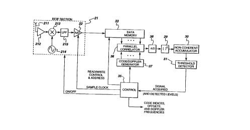
Figure 3 shows a conventional serial acquisition architecture that
uses a serial correlator. In a conventional GPS receiver, signal
acquisition is followed by carrier and PIN code synchronization and
NAV data demodulation, but modules for these processes are not
shown in Figure 3. The signal acquisition architecture comprises an
RF/IF (radio frequency/intermediate frequency) section 21 including an
antenna 211, an RF amplifier 212, a mixer 213 and local oscillator 214,
and a low pass filter 215 which supplies a received and down-
converted signal to analog-to-digital (AID) converter 22. AID converter
22 typically samples and converts at an integer multiple of the replica
CIA code chip rate and supplies a digital sequence to a serial digital
correlator 23. Correlator 23 serially computes the inner product of a
digitized receiver-output sub-sequence from A/D converter 22 and a
C/A replica code sub-sequence originated from a code/Doppler (or
replica) generator 24. The inner product is performed serially by first
multiplying the first terms of the two sub-sequences in a multiplier 231
and storing the result in a coherent accumulator 232, then multiplying
the second terms of the two sub-sequences and adding their product to
coherent accumulator 232, etc. The inner product is performed in real
time, as sub-sequence terms become available from AID converter 22.
As is conventional, the sub-sequences usually span a single period of
the repeating C/A code. After an inner product has been computed, the
CA 02258673 1998-12-17
WO 98/02830 PCT/US97/13201
- 16-
coherent accumulator contains a sample of the cross correlation of the
received sub-sequence with one CIA code cycle of the replica signal,
for the particular C/A code, code-offset and Doppler frequency
generated by the replica generator. The inner product operation is
s repeated with several following sub-sequences from AID converter 22
while using the same replica C/A code sub-sequence. The subsequent
inner product results are then squared by a squarer 29 and summed in
a non-coherent accumulator 30, yielding a non-coherent integration of
the coherent processing results. The output signal of non-coherent
~o accumulator 30 is examined by a threshold detector 31 and a "signal
acquired" command is generated if the signal level in non-coherent
accumulator 30 is sufficiently high. When a signal is acquired, a control
27 monitors the associated CIA code index (satellite index), code
offset, and Doppler frequency, and commands code/Doppler generator
~s 24 to either change to a different C/A code (for a different GPS
satellite) and begin another search, or to stop if sufficient satellite
signals have been acquired. If a signal is not acquired after the several
sub-sequences from AID converter 22 have been processed, then
control 27 commands code/Doppler generator 24 to change to a
2o different C/A code, code offset, or Doppler frequency. As each satellite
signal is acquired, control 27 supplies the associated code index, code
offset and Doppler frequency to GPS signal synchronization and NAV
data processing units (not shown).
Provision for searching all feasible CIA codes, code offsets and
2s Doppler frequencies must be provided. Control 27 selects the desired
CIA code and code offset through commands to a satellite-code
generator 243 and 'offset generator 244. Offset generator 244 provides
for a time offset of the generated code replica from satellite-code
generator 243, relative to the bit stream from AID converter 22. A
3o Doppler I/Q generator 242 generates a digital representation of the
sinusoid representing the combination of Doppler shift and
local-oscillator frequency error assumed by control 27. The replica
signal is generated by a multiplier 241 as the product of this sinusoid
SUBSTITUTE SHEET (RULE 26~
CA 02258673 1998-12-17
WO 98/02830 PCT/US97/13201
- 17-
and the C/A code replica. To insure detection of the GPS signal, the
RF/IF section 21 must generate both an in-phase (I) and a quadrature
(Q) output signal (not shown in Figure 3), and the two signals must be
processed for signal acquisition. Furthermore, each of the I and Q
s RF/IF output signals must be processed with both the I and Q Doppler
sinusoidal components, as is known by those skilled in the GPS art.
The conventional approach shown in Figure 3 requires the
receiver output data from RF/IF section 21 to be processed as soon as
it is available, and processing is constrained by the code rate in the
to received signal. The architecture for an improved sequential signal
acquisition processor according to one aspect of the invention is shown
in Figure 4. The architecture is similar to that of Figure 3 except that a
signal-storage memory 33 is added and power to RF/IF section 21 is
now controlled by control 35. The GPS signal supplied by RF/IF section
Is 21 is converted to digital format by A/D converter 22, but now the A/D
sampling rate may be set at a low non-integer multiple of the C/A code
rate. Memory 33 stores a length of input signal sufficient for signal
acquisition and allows the RF/IF section to be turned off after storage.
The acquisition process then proceeds by reading and possibly re-
2o reading the data stored in memory. Energy consumption is thereby
significantly reduced because the RF/fF section 21 consumes
significant power. Furthermore, acquisition processing is no longer
constrained by the code rate of the received signal, as noted in prior
art. The non-integer input A/D sampling rate allows the acquisition
2s processor to determine accurate GPS signal propagation time
differences (needed for determining the location solution) while using a
much lower sampling rate. Also, when the input SNR is not too low, or
when accuracy requirements are not too high, the low non-integer
sampling rate allows the time differences to be determined with
3o sufficient accuracy that the conventional carrier and PIN code
synchronization processes normally needed (e.g., the Costas phase-
locked loop for carrier tracking, and the early-late delay-locked loop for
code tracking) can be avoided.
SUBSTITUTE SHEET RULE 26)
CA 02258673 1998-12-17
WO 98/02830 PCT/US97/13201
- I8-
An advantage of storing the received signal segment in memory
and re-reading the memory as needed to process different SCD bins is
that the correlation process can take place over a period of time without
loss of signal-acquisition accuracy due to local oscillator instability or
s inaccuracy. Furthermore, if the stored signal is also used to derive the
time delays needed for the navigation solution, there is no need to
maintain accurate timing between the acquisition and tracking phases
of GPS reception. For applications where the navigation solution is not
needed immediately after measurement (e.g., asset tracking), a very
to low power GPS receiver can be constructed by using a very low-power
integration process for the sequential correlator (and other circuits) in
combination with a low-power data storage memory. Very low power
large-scale integration processes are being developed in the industry
(e.g., 1.5v, 0.35 micron complementary metal-oxide-semiconductor or
Is CMOS process).
With the GPS system, as in most DSSS systems, the SNR is
very low before signal processing, and a substantial period of the
received signal must be processed to yield the high SNR correlation
peak needed for reliable signal detection by threshold detector 31. For
zo normal civilian GPS applications, approximately 20ms of signal from the
RF/IF section 21 must be stored and processed. To keep the memory
size small, the signal from RF/IF section 21 is sampled at a low rate
and is quantized to only a few levels. For civilian applications,
conventional GPS receivers typically achieve a GPS fix (location)
2s accuracy of 30 meters. GPS fixes with this accuracy can be calculated
from signal code offsets that are measured with an error of less than
one tenth of a C/A code chip. The signal code offset is measured by
noting the replica-signal code offset associated with the
cross-correlation peak. In one embodiment of the invention, a
3o sequence of results from non-coherent accumulator 30 are generated
in order of increasing replica code-offset while holding the code index
and Doppler frequency constant. If a large correlation result is
observed, an interpolation algorithm is applied to the sequence of
'SUBSTITUTE SHEET (RUtE ~6"~
CA 02258673 1998-12-17
WO 98/02830 PCTIUS97/13201
- 19-
results and the code-offset associated with the correlation peak is
estimated. A code-offset accuracy of one-tenth of a code chip is
achieved while sampling the signal at approximately twice the C/A-code
chip rate. Some conventional GPS receivers don't achieve the desired
s one-tenth chip accuracy during signal acquisition; instead, some do so
during code synchronization by sampling the signal at twice the
C/A-code chip rate and tuning the sampling phase as part of the
early-late delay-locked loop. Alternatively, other conventional GPS
receivers achieve one-tenth chip timing accuracy by sampling the signal
io at ten times the C/A-code chip rate and noting the code offset, in one-
tenth chip increments, that yields the largest correlation peak. A
reduced sampling rate requires less memory and lower processing
rates.
The SNR at the input to A/D converter 22 is well below zero, so
is little signal degradation is suffered when the A/D converter uses just
three appropriately chosen representation levels. Each sample can be
conveniently encoded in sign-magnitude format using only two data
bits. To insure signal detection, bath I and Q RF/IF output signals must
be generated, stored, and processed (only one RF/IF channel is shown
2o in Figures 3 and 4). The use of three or more representation levels can
provide substantial resistance to interference by non-GPS signals, as is
known by those skilled in the GPS art. However, a smaller data
memory is required if only two representation levels (one bit) are used
for the I and the Q signals, and this has a cost advantage in some
2s applications. In one embodiment of the invention, the I and Q RF/IF
output signals are digitized and stored simultaneously, and the data
memory length is sufficient to hold the entire data sequence needed to
achieve acquisition (e.g., 20 ms). With 1023 CIA code chips per
millisecond and both I and Q RF/IF signals being sampled at
3o approximately two samples per code chip with two bits per sample,
approximately 170,000 bits of storage are required for the 20ms signal
segment. For convenience, the I and Q data can be considered as
stored in separate i and Q memories. When the required data has been
SUBSTITUTE SHEET (RULE 26~
CA 02258673 1998-12-17
WO 98/02830 PCT/US97/13201
-20-
sampled, converted, and stored, the receiver can be turned off and the
recorded data can be processed.
In the sequential method of this invention, the stored data is
replayed (read) once during the correlation process for each
s combination of code, code offset, and Doppler shift. In the system of
Figure 4, the sequence of stored digital data samples are read from
memory 33, one at a time. Each sample of the sequence from memory
33 is multiplied by the corresponding sample of the sequence from the
code/Doppler generator 24 in multiplier 231, and the result is
to accumulated in coherent accumulator 232. The sequence or data
segment from the code/Doppler or replica generator is crafted for a
particular code, code offset, and Doppler frequency under test. The
length of the memory sequence so processed is the coherent
integration length, and is typically chosen as one full cycle of the C/A
~s code, which is 1.0 milliseconds (ms). Several (e.g., twenty) adjacent
l.Oms memory data segments are processed in this manner without
changing the replica sequence. After each l.Oms segment is
processed, the value stored in coherent accumulator 232 represents
the cross correlation between the l.Oms replica and data segments
20 (sequences). This value is squared by squarer 29 and added to
non-coherent accumulator 30. Before the first l.Oms segment is
processed for a given replica signal, non-coherent accumulator 30 is
reset to zero so that the final accumulated result represents the total
correlation score for the particular code, code offset, and Doppler
2s frequency specified by the replica signal. Similarly, the coherent
accumulator is reset before each l.Oms segment is processed.
Threshold detector 31 monitors the correlation score and produces a
"signal acquired" signal if the score is larger than a specified threshold.
Upon receipt of a "signal acquired" signal, control 35 performs a simple
3o peak-search and interpolation algorithm (described subsequently) to
find the best estimate of the code offset associated with the given code
index and Doppler frequency under examination. Control 35 then
selects another code, code-offset, and Doppler frequency combination
SUBSTITUTE SHEET (RULE 26)
CA 02258673 1998-12-17
WO 98/02830 PCT/US97/13201
-21-
and commands replica generator to alter the replica signal to reflect this
change. The signal acquisition process is repeated for multiple replica
signals corresponding to the codes, code offsets, and Doppler
frequencies to be searched, and is stopped when the desired number
s of GPS signals (different C/A codes) have been acquired. Control 35
then produces as an output signal the code indices, estimated offsets,
and Doppler frequencies associated with the acquired signals.
The I and Q memory data can be processed sequentially, (e.g.,
process all I data, then process all C~ data) using one digital correlator
~0 23 as shown in Figure 4. Alternatively, the I and Q memory data can be
processed simultaneously using separate digital correlators. In any
event, to insure signal acquisition, I and Q Doppler processing must be
performed on both the I memory data, and the Q memory data. Thus
there are four I-Q combinations and they can be processed sequentially
~s with a single digital correlator, or simultaneously with multiple
correlators. In one sequential method, the correlation result for the full
memory data sequence with a given replica code index, code offset,
and Doppler frequency is calculated as follows: First, the coherent and
non-coherent accumulators are reset to zero. Then the I memory data
2o is processed with the I Doppler replica and the correlation result is
accumulated in the coherent accumulator. The Q memory data then is
processed with the Q Doppler replica and the correlation result is
further accumulated in the coherent accumulator. The total
coherent-accumulation result is then squared by squarer 29 and added
2s to non-coherent accumulator 30. The coherent accumulator is then
reset. Next the Q memory data is processed with the I Doppler replica
and the correlation result accumulated in the coherent accumulator,
then the I memory data is processed with the Q Doppler replica and the
correlation result is inverted (multiplied by -1 ) and further accumulated
3o in the coherent accumulator. The total coherent-accumulation result is
then squared by squarer 29 and added to non-coherent accumulator
30. This process is repeated for each l.Oms memory data segment,
without resetting the non-coherent accumulator between segments, and
SUBSTITUTE SHEET (RULE 26)
CA 02258673 1998-12-17
WO 98/02830 PCT/US97/13201
-22-
requires two full read cycles of both the I and Q memory data.
Acquisition time and energy can be reduced by using separate I and Q
Doppler generators 242, multipliers 241, and digital correiators 23 to
process all four I-Q combinations simultaneously.
s In one convenient rendition, code/Doppler generator 24 is
comprised of Doppler I/Q generator 242, satellite code generator 243,
offset generator 244, and multiplier 241, as shown in Figure 4. Doppler
I/Q generator 242 generates a digital sequence representation of a sine
or cosine wave at the desired frequency relative to the sample rate, and
~o can, for example, be implemented with a Read Only Memory (ROM)
driven by an address counter. The frequency and phase (I or Q) of the
sinusoid can be selected by control of the order in which the stored
sinusoidal samples are read (e.g., by address decimation and by
selection of the starting address, respectively). Other digital sinusoid
Is generators are also known to those skilled in the art. For the GPS C/A
codes, a well known state machine can be used to generate the C/A
code bits in the proper order. The Doppler sinusoid and C/A code
values are multiplied by multiplier 241 to yield the replica signal.
Provision for searching all feasible code offsets is provided by a time
20 offset of the stored code replica from satellite code generator 243 using
offset generator 244. With the state-machine implementation of
satellite-code generator 243, a particular code offset is effected by
presetting the state machine to the associated state before starting the
correlation process. The initial states, corresponding to different code
2s offsets, can be stored in a ROM and indexed by a simple binary
address counter.
In practice, the acquisition search is conveniently performed by
first selecting a code and a Doppler frequency, and then indexing
through different code offsets. Then the Doppler frequency is changed
3o and the different code offsets are re-examined. Non-coherent
accumulator 30 can be implemented as an array of accumulators, one
for each candidate code offset in a sequence of adjacent offsets. This
accumulator organization allows the scores for adjacent offsets to be
SUBSTITUTE SHEET (RULE 26~
CA 02258673 1998-12-17
WO 98/02830 PCT/US97/13201
-23-
simultaneously examined so that an interpolation algorithm can be
applied to find the sub-chip offset value associated with the actual
score peak. if a sequential interpolation algorithm is used, the peak
offset value can be interpolated while using only a single accumulator
s element.
The total acquisition time can be reduced by processing multiple
code offsets simultaneously. For example, multiple digital correlators 23
can be used, each driven with a differently delayed version of the
replica signal. The different delays can be implemented with a tapped
io delay line coupled to the output of code/Doppler generator 24. The
different taps can then each drive a separate serial digital correlator 23,
and the results from each correlator can be separately squared and
accumulated in associated elements of a non-coherent accumulator
a rray.
is An alternative GPS receiver architecture that provides for both
low-power and fast signal acquisition, according to another aspect of
the invention, is shown in Figure 5. The acquisition architecture is
similar to that of Figure 4, except that the serial digital correlator, serial
Doppler and P/N code generators, and serially read memory are now
2o replaced with a parallel correlator 36, parallel Doppler and P/N code
generators 37, and a parallel read memory 33, respectively. One
aspect of the invention is a method for massively parallel analog
summation in the parallel correlator. The analog summation, in
combination with the massively parallel organization of the memory,
2s replica-generator, and correlator elements, provides for the dramatic
time and energy reductions in the correlation process. The analog
summation result is converted to digital form by A/D converter 38 which
may be combined with squarer 29, as described subsequently. The
parallel architecture also takes advantage of conventional low-power
3o complementary metal oxide semiconductor (CMOS) integrated circuit
technology to achieve low-energy use. Energy use in CMOS circuits is
dominated by the charging and discharging of circuit node
capacitances; little energy is used at nodes whose voltages are static
SUBSTITUTE SHEET (RULE 26~
CA 02258673 1998-12-17
WO 98/02830 PCT/US97/13201
-24-
(unchanging) or whose capacitance is small. With this invention the
Doppler and P/N code replica generators and registers, data memory,
and parallel correlator are organized to minimize the number of CMOS
nodes being charged and discharged during the correlation process.
s Figure 6 illustrates the parallel correlation concept and shows
waveforms for the case where the received and replica signals have no
Doppler shift. Digitized signal data is written sequentially into the data
memory as it becomes available from the RF/IF section 21 and A/D
converter 22. Data memory 33 is organized for a massively parallel
to output so that a long sequence of data is available at the output
simultaneously. Also, a shift register 1004 is loaded with the chosen
replica signal and is organized for a massively parallel output with the
same length as that from the data memory. A sample of the cross-
correlation (i.e., the inner product) between the parallel data sequence
is and parallel replica sequence for a given Doppler frequency, code
index and code offset is generated all at once by parallel correlator
1000. In parallel correlator 1000, each element of the memory data
sequence is multiplied by the corresponding element of the replica
sequence using a corresponding multiplier in an array of multipliers.
2o The multiplier output signals are simultaneously summed to form the
coherent processing result at the correlator output. The coherent
processing result for an adjacent code offset is generated by shifting
the replica register one step while holding the memory data stationary.
Alternatively, the replica signal can be held stationary while the memory
25 data is shifted.
In one attractive embodiment of the invention, the parallel-output
data and replica sequences are l.Oms long and span a single cycle of
the C/A code. The data sequence is generated from the RF/IF output
signal by sampling at the rate of approximately two samples per C/A
3o code chip and digitizing to three levels with an AID converter using a
two-bit sign-magnitude format. This sampling rate and number of levels
avoids abasing, avoids substantial SNR degradation if the A/D
threshold levels are properly chosen, and yields sequence lengths on
SUBSTITUTE SHEET (RULE 26)
CA 02258673 1998-12-17
WO 98/02830 PCT/ITS97/13201
-25-
the order of 2100 samples. The sign-magnitude format allows a simple
multiplier to be used in the multiplier array described above. Other
attractive data representations, sampling rates, and parallel-output
sequence lengths are possible, as will become apparent to those skilled
s in the art.
Figure 7 shows one method for generating the parallel-output
replica sequence. In a code/Doppler generator 1008, a C/A code
generator 1001 generates the desired C/A code sequence and a
digitized sinusoid generator 1002 generates the digitized sinusoid
io sequence with the desired phase and Doppler frequency. A multiplier
1003 sequentially multiplies the code and sinusoid sequences provided
by code/Doppler generator 1008 to generate the replica sequence, and
this sequence is shifted into a parallel-output code/Doppler (replica)
register 1004.
~s The replica sequence is preferably represented in three level
(two-bit) sign-magnitude format, or a two-level (one-bit) sign format, as
these formats reduce the complexity and power consumption of the
parallel correlator with respect to a format that uses more bits. With
only three or fewer levels, the Doppler component in the replica
2o sequence will have high harmonic content and these harmonics can
falsely correlate with an input signal. This problem can be avoided by
choosing the RF/IF local oscillator frequency so that the RF/IF output
signal is substantially offset from zero frequency. By choosing the offset
large enough, the harmonics of all resulting necessary Doppler-replica
2s frequencies will be well above the highest Doppler replica frequency.
The harmonic problem is known by those skilled in the design of
superheterodyne receivers. If desired, the Doppler-replica harmonic
levels can be reduced by using more bits in the Doppler and replica
sequence representation and more bits per sample in the replica
3o register. However, this will increase the power consumption and
complexity (size) of the signal-acquisition implementation.
Figure 8 shows a short segment of an embodiment of the data
memory 33, replica shift register 1004, and parallel correlator 1000 that
SUBSTITUTE SHEET (RULE 26)
CA 02258673 1998-12-17
WO 98/02830 PCT/US97/13201
-26-
uses the replica generation method of Figure 7. Both the data and
replica sequences use a two-bit sign-magnitude representation, and
since the rows of elements in each of memory 33, shift register 1004,
and correlator 1000 are aligned with each other in columnar fashion the
s sign (S) and magnitude (M) bits of corresponding samples from the two
sequences can be conveniently fed, in each column, to a
corresponding multiplier 1200. With sign-magnitude input values of, for
example, either -1, 0, or 1 from the two input sequences, each
multiplier 1200 generates either -1, 0, or 1 as an output signal. A
io separate digital-to-analog converter 1300 converts each digital
multiplier output signal to analog form. All D/A converter output signals
are summed by being furnished to a common output that represents
the analog correlation result. The analog summation is conveniently
implemented using charge summation, but alternative analog
~s summation forms are also possible. This summation method is spatially
efficient, requires very low power, does not require any analog memory,
and is very fast. Another advantage of this parallel correlator
architecture is that the code and Doppler sequences are
programmable, allowing a single correiator to rapidly search over
2o multiple code indices, offsets, and Doppler frequencies in the
acquisition process.
Figure 9 shows one embodiment of one stage of the
two-sequence parallel correlator of Figure 8. Multiplier 1200 generates
sign and magnitude output bits that control switches 1400 and 1500 in
2s a D/A converter 1300. The switches connect one end of a charge
summation capacitor 1100 to either a positive reference voltage rail or a
negative reference rail, or to an output reference voltage rail (e.g.,
ground). The sum is generated by a two step procedure. Fiirst the
charge-reset line is set low, closing a charge reset switch 1600 and
3o forcing switch 1400 in each parallel correlator stage to connect the
associated capacitor to the output reference rail (ground in Figure 9).
This discharges all capacitors. Then the charge reset line is set high,
opening charge reset switch 1600 and allowing the data and replica
SUBSTITUTE SKEET (RULE 26~
CA 02258673 1998-12-17
WO 98/02830 PCT/US97/13201
-27-
values in each parallel correlator stage to control the associated sign
and magnitude switches, 1500 and 1400, respectively. This two-step
process insures that excess charge does not accrue on the charge
summation capacitors over time. It is advantageous that this parallel
s correlator can be implemented in low-cost digital processes by using,
for example, metal-metal "cross-aver" capacitors and binary electronic
switches. Finally, it is advantageous that the charge summation can be
extended across multiple integrated circuits by simply extending the
summation lines.
io Figure 10 shows another method for generating the replica
signal. With this method, the code and Doppler replica sequences are
stored in separate parallel-output registers. C/A code generator 1001 of
code/Doppler generator 1010 generates the desired CIA code
sequence and this sequence is shifted into a code replica register
Is 1005. Similarly, a digitized sinusoid generator 1002 of code/Doppler
generator 1010 generates the digitized sinusoid sequence with the
desired phase and Doppler frequency, and 'this sequence is shifted into
the Doppler replica register 1006.
Figure 11 shows an embodiment of the data memory 33,
zo code-replica register 1005, Doppler-replica register 1006, and parallel
correlator 1000 that uses the replica generation method of Figure 10. A
separate code register 1005 and Doppler register 1006 are used,
yielding separate memory-data, code, and Doppler sequences. Sign (S)
and magnitude (M) bits of corresponding samples from the three
2s sequences are fed to corresponding multipliers 1201. With
sign-magnitude input values of, for example, -1, 0, or 1 from the data
and Doppler sequences, and -1 or 1 from the code sequence, each
multiplier 1201 generates either a -1, 0, or 1 as an output signal. The
different multiplier output signals are all simultaneously summed using
3o analog summation as previously described for the two-sequence
parallel correlator.
- Figure 12 shows one embodiment of one stage of the
three-sequence parallel correlator of Figure 11. The correfator stage
SUBSTITUTE SHEET (RULE 26)
CA 02258673 1998-12-17
WO 98102830 PCT/US97/13201
_?g_
shown is similar to that of the two-sequence parallel correlator of Figure
9 except that the multiplier has an extra exclusive-or gate 1205 to allow
the separate code register bit to impact the sign of the multiplication
result.
s The two and three sequence parallel correlators of Figures 8 and
11 can be generalized to plural sequence parallel correlators. With
respect to the two sequence correlator, the three sequence correlator
has had one of the cross-correlation sequences (the replica)
decomposed into two separate sequences. This decomposition can be
~o applied to both the data and replica sequences in general to provide a
plural sequence parallel correlator or inner-product machine.
"Differential" analog summation in the parallel correlator may
have lower noise susceptibility and other advantages. Figure 13 shows
one convenient differential summation configuration. In each stage of
~s the parallel correlator, two D/A converters are driven in parallel by the
same sign and magnitude output signals from the associated multiplier.
One converter is labeled as positive and its capacitor connects to a
positive summation line and the other converter is labeled as negative
and its capacitor connects to the negative summation line. The
2o switches shown in each converter are implemented as electronic
switches, as is well-known in the art. The two converters operate
identically except that the sign switch 1500 in the negative converter is
connected in the reverse sense with respect to the sign switch of the
positive converter. With the differential method, the difference between
2s positive and negative summation results must be taken to determine
the final coherent correlation result. This can be performed by, for
example, using a high-speed linear or switched capacitor difference
amplifier, as is known by those skilled in the art. Alternatively, the
positive and negative summation results can be separately A/D
3o converted and then their difference computed digitally prior to squaring
and non-coherent accumulation.
The three-sequence parallel correlation method of Figure 11
uses less power than the two-sequence method of Figure 8 because
~SUBST1TUTE SHEET (RULE 26)
CA 02258673 1998-12-17
WO 98/02830 PCT/US97/13201
-29-
only the 1-bit deep code register needs to be shifted when developing
correlation results for subsequent code offsets; the sequence in the
separate Doppler register can be held fixed. Shifting a register that is
two bits deep consumes approximately twice the power as shifting a
s register that is one bit deep. Because register shifting is a dominant
power consumer with the parallel correlation approach, the
three-sequence method is advantageous. On the other hand, the two
sequence method uses fewer shift register elements (bits) and fewer
exclusive-or gates in the multipliers and therefore has a smaller
io implementation. The implementation size difference diminishes as the
number of bits of Doppler replica representation is increased.
D/A converters 1300, shown in Figures 9 and 12, utilize series
switches to control charging of the charge summation capacitors. An
alternative embodiment for the multiplier and analog converter (D/A) is
is shown for the three-sequence case in Figure 18. An advantage of this
embodiment is that digital logic functions directly drive the charge-
summation capacitors and a series connection of switches is not
needed. This multiplier-D/A combination is readily implemented in a
standard digital CMOS process. Capacitors 1101 and 1102 are of
zo substantially the same value and together provide for a three-level D/A
conversion, e.g., -1, 0, and +1. The -1 level is invoked by driving both
capacitors low (digital ground), the +1 level is invoked by driving both
capacitors high (digital Vdd), and the 0 level is invoked by driving one
capacitor high while driving the other low. In a multiplier 2001, exclusive
2s NOR gate 1210 and AND gate 1211 multiply the two-bit data and
Doppler values to form the sign-magnitude product. Exclusive NOR
gate 1212 then converts the two-bit product to A and B signals that
drive the two capacitors in either the same or different directions.
Finally, exclusive NOR gates 1213 multiply the A and B signals by the
3o binary code value, while NOR gates 1214 provide for grounding the
capacitors so as to discharge them during the reset phase.
For a given length of stored GPS signal, a tradeoff exists
between the length of coherent and non-coherent processing. As the
SUBSTITUTE SHEET (R!!l..F 26)
CA 02258673 1998-12-17
WO 98/02830 PCT/US97/13201
_30_
coherent correlation length is increased, the SNR of each coherent
processing result is increased but the number of coherent processing
results available for squaring and non-coherent accumulation
(integration) decreases. It is known by those skilled in the art that the
s SNR improves by 10 dB per decade of coherent processing length
increase, but increases by only about 5 dB per decade of non-coherent
processing length. Thus, for a given memory data length, the
pre-detection SNR is maximized by performing one long coherent
correlation. However, unpredicted receiver motion or local oscillator
io fitter will limit the feasible length of coherent processing. Also, as the
coherent correlation length is increased, the bandwidth of the Doppler
bins is reduced and this yields more Doppler bins that must be
searched. The architectures of Figures 4 and 5 readily allow dynamic
trading of coherent and non-coherent processing length through control
is of the replica generator, resetting of the coherent and non-coherent
accumulators, and bypassing of the squaring functions.
It is usually true that the pre-detection SNR needed for reliable
detection is lower than the SNR needed for accurate correlation peak
localization (i.e., interpolation). Thus the acquisition time and energy
2o can be minimized by using shorter coherent correlations (and thus
searching over fewer Doppler bins that are as wide as the detection
reliability constraints will allow) until a correlation detection is observed,
and then reprocessing the data with longer coherent correlation using
code offsets and Doppler shifts near the values that yielded the
2s detection event, to increase the SNR and perform superior code offset
interpolation. The architectures of Figures 4 and 5 readily allow this two
step process.
Figure 14 shows a section of the noiseless auto-correlation
waveform for a 1.0 ms CIA-code PIN waveform (not sampled). The
3o auto-correlation value is very near zero for all offsets of magnitude
greater than one chip width and is a triangle function (of the offset) for
offsets between -1 and +1 chip width. In another aspect of the
invention, accurate sub-chip correlation-peak time estimation is
SUBSTITUTE SHEET (RULE 26)
CA 02258673 1998-12-17
WO 98/02830 PCT/US97/13201
-31-
achieved without using sampling rates that are substantially higher than
twice the CIA chip rate by using a sampling rate that is a non-integer
multiple of the CIA chip rate. With an integer number N of samples per
ClA code chip, the discrete-time auto-correlation sample value remains
s substantially constant over an input-signal time offset variation of 1/N of
a C/A code chip period when the receiver bandwidth is substantially
wider than the GPS signal bandwidth. This is a form of quantization and
yields substantial quantization error if N is not large. For example, an
offset measurement accuracy of one-tenth of a C/A code chip would
~o require a sampling rate of N=10 times the CIA code chip rate. With a
more-limited receiver bandwidth, the auto-correlation sample value
varies with input-signal time offset, but not necessarily linearly with
input offset. If a non-integer multiple sampling rate is used, then the
sample instants precess or roll in chip-relative position as a sequence
is of signal C/A code chips is sampled. This precession allows the
calculated auto-correlation value to change substantially linearly with
input-signal time shift, and with much smaller time shifts. Although the
above discussion has focused on the auto-correlation of the binary CIA
code, the sample precession method is applicable to multiple-level
2o signals in general.
With a replica code index and Doppler frequency that matches
that of a noisy input signal, the serial or parallel correlator will calculate
noisy samples of the shown auto-correlation function. By choosing the
signal sampling rate so that there is an integer number of samples
zs (e.g., 2183) per l.Oms CIA code period, correlation results from, for
example, twenty consecutive 1.0 ms data memory sequences (using
the same replica code offset) will yield twenty noisy samples of the
same point on the CIA-code auta-correlation waveform. During signal
acquisition, the replica Doppler frequency and phase rarely match that
30 of the signal exactly so that squaring of the coherent correlation result
is necessary to guarantee a positive correlation result. Figure 14 also
shows typical squared l.Oms coherent correlation sample points (x)
calculated for several code offsets near that of the received signal, and
SUBSTITtlTE SHEET (RULE 26)
CA 02258673 1998-12-17
WO 98/02830 PCT/US97/13201
-32-
with code index and Doppler frequency and phase that match that of
the input signal. By averaging the squared samples from the same
code offset, a lower-noise estimate of the corresponding
auto-correlation value is generated. Typical averaged auto-correlation
s samples are also shown in the figure. This averaging is the so-called
non-coherent accumulation. The phase of.the sample grid, relative to
the triangle function, depends on the phase of the received waveform
relative to the input AID sampling clock.
In the waveform of Figure 14, the time of the auto-correlation
to peak is a parameter of interest, and this peak time is usually not on the
sampling grid. However, using the averaged auto-correlation values
surrounding the peak time, the peak time can be estimated by
interpolation. Various interpolation methods are known to those skilled
in the art, but one method involves ordering the averaged
is auto-correlation samples according to increasing code offset and then
searching for the two largest adjacent entries. The left entry (the earlier
one) and its left neighbor (points B and A respectively in the figure)
together define a line, while the right entry and its right neighbor (points
C and D respectively in the figure) together define another line. These
2o two lines intersect somewhere between the two original end points (A
and D in the figure) when the SNR is high enough, and the time
associated with this intersection is the estimated correlation peak time.
This method requires solution of two simultaneous equations, may be
used with either the serial or parallel correlator methods, and would be
2s computed by control 35 shown in Figure 4 or Figure 5.
Figure 15 shows a low-power parallel-correlator based acquisition
system with full I/Q processing in which the RF/IF section (not shown)
generates two quadrature output signals which are passed to input AID
converters 22 and 56. Control 35 applies power to the RF/IF section and
3o to input AID converters 700 and 701. A/D converter 56 generates
sampled I data which is stored in the data I memory, while AID converter
22 generates sampled Q data which is stored in the data Q memory.
SUBSTITUTE SHEET (RULE ?6)
CA 02258673 1998-12-17
WO 98/02830 PCT/US97/13201
-33-
In one embodiment of the system, the input A/D converters
sample the I and Q input signals periodically at approximately 2.183
million samples per second, yielding 2183 samples per C/A code cycle
and approximately 2.1 samples per C/A code chip. The samples are
s quantized to 3 levels and use two-bit sign-magnitude representation, as
described earlier. The I and Q data-storage memories are each large
enough to store the entire data segment needed for signal acquisition.
For nonmilitary utilization, this is usually 20 ms. After 20 ms (2183 x 20
samples) of I and Q data have been stored, power is removed from the
to RF/1F section and from the input A/D converters, and acquisition
processing is begun. The I and Q data memories are each organized as
twenty rows of 2183 two-bit samples, with 2183 simultaneous outputs
(one full row). Four separate three-sequence parallel correlators are
used, labeled II, IQ, QI, and QQ. Together these comprise a complex
~s parallel correlator 70. The parallel correlators each use sequence
lengths of 2183 samples. The I data memory drives the II and IQ
correlators, while the Q data memory drives the QI and QQ correlators.
Also, the I Doppler register drives the II and QI correlators while the Q
Doppler register drives the IQ and QQ correlators. The order of data
2o processing is set so that all desired replica code offsets are examined
for a given replica code index and Doppler frequency before the code
index or Doppler frequency is changed. Furthermore, all desired code
offsets are processed for a given row of stored I and Q data before the
row is changed. This will most likely minimize the combined memory
2s reading and code-register shifting energy use. Other memory-row,
code-index, and Doppler frequency processing orders are also possible,
and the order can be chosen to minimize energy consumption. The II
and QQ coherent processing results are summed to form II+QQ by
connecting the associated summation lines, and the Ql and IQ coherent
3o processing results are summed by connecting their associated
summation lines. For proper I-Q processing, either the QI or the IQ
result must be inverted, and this can be accomplished by, for example,
SUBSTITUTE SHEET (RULE 26)
CA 02258673 1998-12-17
WO 98/02830 PCT/US97/13201
- 34 -
reversing the sense of all sign switches in all analog converters of the
chosen parallel correlator. In this embodiment, IQ-QI is formed.
With GPS signals, the SNR of each II+QQ and IQ-QI signal is
typically 0 to 4 dB. These signals are adequately represented with only a
s few levels (e.g., -1, 0, 1 ) and are converted to digital form by A/D
converters 700 and 701, and then separately squared by squarers 702
and 703. The squared signals are summed by digital adder 46 and
stored in accumulator 44. Accumulator 44 has a separate storage
position associated with each candidate code offset, and correlation
io results for each code offset with different received data segments are
accumulated in the associated storage position.
Figure 16 shows one embodiment of a squaring flash A/D
converter that combines the A/D and squaring functions. Here two
comparators 61 and 62 determine if the analog value is above, below, or
is between the two threshold values associated with analog representation
levels -1, 0, +1. A logic unit 63 then maps the comparators' joint output
state to the appropriate squared digital value. If desired, this squaring
flash converter is readily generalized to more than three representation
levels by adding more comparators and threshold voltages.
2o The sampling rates, stored sequence lengths, and simultaneous
memory outputs lengths can be chosen to best fit the GPS application.
For example, by storing the entire data segment needed for signal
acquisition, the RF/IF section can be turned off after the shortest
possible time (commensurate with receiving the needed data segment).
2s The stored data set can then be used for the processing of all SCD bins
in the acquisition search. Alternatively, a shorter memory can be used at
the expense of having to keep the RF/IF section on for a longer time.
For example, another attractive embodiment uses a "Ping-Pong"
memory organization and is illustrated in Figure 19. Here, the I and Q
3o data-storage memories 192 and 194, respectively, are each only 2.0 ms
long and are organized as two parallel-output 1.0 ms rows (e.g., 2183
samples in each row, as before). In both the I and Q data channels, one
data row is accessed in parallel, for parallel correlation, while the other
SUBSTITUTE SHEET {RULE 26)
CA 02258673 1998-12-17
WO 98/02830 PCT/US97113201
-3s-
data row is being written with digitized data arriving from the RF/IF
section. The entire I and Q data sequence lengths are each processed
in 1.0 ms segments. The entire 20 ms data set is then processed for a
single SCD bin in approximately 20 ms. Because the entire data
s sequence was not stored, the RF/IF section must be energized and
produce another entire sequence if another SCD bin is to be tested. On
the average, this increases the time that the RF/IF section must be kept
energized during signal acquisition. However, the reduction in memory
size can be dramatic. In some applications (e.g., military receivers under
io severe jamming conditions), the GPS SNR is very low and the data
sequence length needed for acquisition may be so long that storage of
the entire sequence is impractical. Under such circumstances, the Ping-
Pong acquisition architecture is advantageous.
In some applications it wilt be advantageous to further reduce the
Is size of the data-storage memories. With the two-segment (Ping-Pong)
memory organization, a long continuous stream of receiver-output data
can be processed. At the expense of a longer time to acquisition, the
two-segment I and Q data memories 192 and 194 (Figure 19) can be
reduced to single-segment memories by eliminating one of the 1.0 ms
2o sections from each memory. With this reduction, time-adjacent 1.0 ms
receiver-output segments are not processed. Instead, only every other
1.0 ms segment is captured in memory and processed, and this
lengthens the time elapsed for processing a given number of received
signal segments.
2s To further reduce the memory size and the complexity of the
parallel correlator, the length of the parallel correlator and the
associated registers and memory segments can all be made smaller
than the desired coherent processing length. The desired coherent
processing length can be achieved by processing multiple shorter data
3o segments and coherently combining their results. For example, a 1.0 ms
coherent processing length can be achieved by using a single 0.5 ms
long parallel correlator on two adjacent 0.5 ms data segments and
adding their results digitally, after AID conversion. Various combinations
SUBSTITUTE SHEET (RULE 26~
CA 02258673 1998-12-17
WO 98!02830 PCT/US97l13201
-36-
of correlator length, coherent processing length, numbers of memory
segments, and code-offset search width are possible.
When the cost, size, and power dissipation of a standard serial
input serial-output (SISO) memory are sufficiently low, it may be
s advantageous to store the entire necessary I and Q data sequences in
such memory, turn off the RF/IF receiver section, and use this memory
in combination with the Ping-Pong or single-segment memory
architectures to examine all desired SCD bins. The entire I and Q data
sequences are read from the SISO memory once for each SCD bin
~o tested, and this reading process will consume energy. However,
because the RF/IF section is turned off, the system energy use will be
reduced if the power dissipation of a SISO memory is sufficiently low
relative to that of the RF/IF receiver section. Other stored sequence
lengths, simultaneous memory output lengths, and sampling rates are
~s also attractive.
In the two-sequence or three-sequence parallel correlator
embodiments of Figures 8 and 11, the product of associated data and
replica samples is performed in parallel within the correlator. This allows
different Doppler bins to be tested for acquisition without having to
zo collect new received data. Figure 20 shows an alternative embodiment
of one stage of a parallel correlator and the associated parallel memory
where the data and Doppler samples are multiplied together by
multiplier 2001 prior to storage in the parallel memory 2002. This is
advantageous because the multipliers in the parallel correlator are thus
2s simplified. Each correlator multiplier now multiplies its associated stored
sample by just a single associated code bit. The combined multiplier and
D/A converter for this correlator embodiment is similar to that shown in
Figure 18, except that the data-Doppler multiplier and A-B signal
converter, comprised of exclusive NOR gates 1210 and 1212 and AND
3o gate 1211, is moved out of the correlator and ahead of the data
memory. The disconnected inputs .to exclusive NOR gates 1213 are
coupled to the data memory outputs. With this embodiment, new data
SUBSTITUTE SHEET (RULE 26)
CA 02258673 1998-12-17
WO 98/02830 PCT/US97/13201
-37-
must be stored if a different Doppler bin is to be tested for acquisition,
but this is not a disadvantage in some applications.
The combined parallel correlator and parallel memory shown in
Figure 20 can be advantageously used to form a simplified full I-Q
s processing GPS acquisition engine. In the full I-Q acquisition engine
shown in Figure 19, there are four separate parallel correlators coupled
to data I and O and Doppler I and Q registers (parallel memory), as well
as to the parallel code register. An alternative full i-Q embodiment that
uses the simpler correlator and memory organization of Figure 20 is
to shown in Figure 21. In this embodiment, the four parallel data-Doppler
memories hold the II, GHQ, IQ and QI data-Doppler product sequences,
respectively. Each parallel memory can be organized as a Ping-Pong or
single-segment memory, as described earlier. There is no separate data
and Doppler storage. Each parallel memory connects to an associated
is parallel correlator, and each parallel correlator also connects tv the
single parallel code register. l-he reduced interconnection between
memory sections and correlator sections allows this full I-Q processor
embodiment to have a simpler (i.e., smaller and less costly) integrated-
circuit implementation.
2o The complexity of the embodiment of Figure 21 can be still further
reduced by performing the II+QQ addition and the QI-IQ subtraction
before data storage. Prior to storage, the addition and subtraction output
signals can often be rounded or truncated to two bits with little SNR
degradation. Then, as shown in Figure 22, only two data-Doppler
2s memories (one for II+QQ data, the other for OI-IQ data), two parallel
correlators, and one code register are needed. Each data-Doppler
memory can be organized as a Ping-Pong or single-segment memory,
as described earlier. Other organizations of the parallel correlator,
parallel memory, and the sequence multiplications are also possible and
3o advantageous.
Figure 17 shows a combined data-memory, replica-generation,
parallel-correlator organization (for just the II correlation process) that
reduces the number of code register shifts to 2183 shifts per
SUBSTITUTE SNEET (RULE 26)
CA 02258673 1998-12-17
WO 98/02830 PCT/US97/13201
-38-
code/Doppler combination and eliminates need for any non-coherent
accumulation RAM. The trade-off is that the input memory must now be
segmented to allow all stored data to be simultaneously accessed.
These data are applied, in 1.0 ms blocks, to separate parallel
s correlators. These parallel correlators are all driven by the same code
and Doppler replicas, and they simultaneously (in one full code cycle)
generate the twenty separate 1.0 ms correlation sequences that were
previously accumulated time sequentially. Separate squaring A/D
converters convert the analog correlation sequences to digital form
io where an adder tree 80 forms the accumulated correlation sequence.
The accumulation RAM can be completely avoided by performing the
peak search and interpolation process on the accumulated correlation
as it is being generated. In this arrangement, the code and Doppler
registers now drive twenty loads where they previously drove one,
~s which may negate some of the energy reduction.
When the parallel correlator is used with data and replica
registers for the two-sequence case, or with data, Doppler, and code
registers for the three-sequence case, it is advantageous to minimize
the energy used in loading (writing) the various registers. In another
2o aspect of the present invention, loading of the various registers is made
a low energy operation by using a scanner shift register to determine
which data, Doppler, and code register stages are to be written at each
instant. Figure 23 shows a scanner shift register 304 in combination
with the data register 300, Doppler register 301, and code register 302
2s for the three-sequence case. In one method of operation, samples
arrive sequentially for each of the digital data, Doppler, and code
sequences and the sample rates are the same. As the samples for
each respective sequence arrive, they are written into corresponding
sequential locations in their respective registers. In synchronism with
3o the arriving samples, a single logical 1 is shifted along the binary
scanner register, enabling the writing of the arriving samples into
corresponding sequential locations of the respective registers. The
writing operation is very low energy because only two adjacent scanner
SUBSTITUTE Sf-IEE'1' (R! ~f_F 2f)
CA 02258673 1998-12-17
WO 98/02830 PCT/US97/13201
-39-
register locations change their stored value at each shift, and none of
the respective registers is shifting during the writing operation.
While the disclosed invention is applicable to GPS C/A signal
acquisition, it can also be used to dramatically reduce both the time and
s energy required to directly acquire the P(Y) military GPS signals without
first acquiring the C/A signals. By altering the satellite-code generator
component of the code/Doppler generator in Figures 4 or 5 to generate
the P(Y) code instead of the C/A code, the methods and architectures
disclosed herein become applicable to the P(Y) case.
io While only certain preferred features of the invention have been
illustrated and described, many modifications and changes will occur to
those skilled in the art. It is, therefore, to be understood that the
appended claims are intended to cover all such modifications and
changes as fall within the true spirit of the invention.
SUBSTITUTE SHEET (RULE 21