Note: Descriptions are shown in the official language in which they were submitted.
CA 022~8779 1998-12-18
:
SPECIFICATION
TITLE OF THE INVENTION
Ultraviolet Absorbing Material and Ultraviolet Absorbing Plate
Technical Field
Generally, there have been employed two methods for providing
a substrate such as a glass sheet with ultraviolet absorbing properties,
one of which to coat a substrate with an ultraviolet absorbing material
and the other of which to utilize multi-reflections of a multilayer. The
latter is excellent in free adjustability of wavelength to be shielded and
capability of clear-cutting, but has a problem relating to cost due to the
complicated production processes. In the former method, there may be
used an inorganic or organic ultraviolet absorber.
Inorganic ultraviolet absorbers as disclosed in Japanese Patent
Laid-Open Nos. 5-339033, 5-345639 and 6-56466 are excellent in
resistance to weathering and resistance to heat but are
disadvantageous because these absorbers are less selective because
the wavelength of ultraviolet to be absorbed is determined by the band
gap of a compound forming the absorbers and none of these can cut off
uitraviolet rays of waveiengths of neighborhood of 400 nm.
Furthermore, most of the absorbers are involved with unexpected
coloration upon interception of ultraviolet rays of longer wavelength.
On the contrary, organic ultraviolet absorbers are broad in range
of absorptivity and thus can absorb ultraviolet in a wide range of
wavelengths by selecting the type, concentration and thickness of the
absorbers. As a result of extensive research directed to a system
having such organic ultraviolet absorbers, it has now been found that
use of an absorber which has a maximum absorption wavelength in a
' CA 022~8779 1998-12-18
~. ~
longer wavelength region or which is increased in concentration or in
layer thickness is conducive to intercept ultraviolet in a longer
wavelength region. However, such an absorber having the maximum
absorption wavelength in a longer wavelength region as disclosed in
Japanese Laid-Open Publication No. 6-145387 is poor in resistance to a
light and reduced in absorbing power with the lapse of time. This
absorber also has a problem that the permeability is easily deteriorated
due to use of a fluorescent bleach.
A benzophenic- or benzotriazolic absorber is relatively good in
resistance to a light and capable of absorbing ultraviolet rays in a
relatively longer wavelength by increasing the concentration and the
layer thickness. However, in the case of coating these absorbers
mixed with a resin over a substrate, the layer formed thereover is limited
in thickness to an extent of several tens of micrometers. However, with
the layer of the mixture in this order of thickness, it is necessary to add
the absorbers in a considerably high concentration. Still, the mere
addition of the absorbers in a high concentration leads to problems
involving deposition thereof and bleedout due to the use over an
extended period of time.
It has been attempted for solving these problems to react an
absorber with a resin in which instance the absorber is copolymerized
with an acrylic resin, as disclosed in Japanese Patent Laid Open
Publication Nos. 2-248412 and 6-88064. However, since the acrylic
resin per se has a drawback in resistance to weathering and heat, the
resulting ultraviolet absorber can not bear to be used over a prolonged
length of time. Alternatively, various researches have been made on
the possibility of using an ultraviolet absorber which is reactive a
... .
CA 022~8779 1998-12-18
-- . .
silicone resin excelled in resistance to weathering and resistance to
heat as disclosed in Japanese Patent Laid-Open Publication No. 61-
54800, 2-117928 and 3-45094. It, however, has been found that most
of such absorbers have a difficulty in synthesis in technical view and a
problem in durability.
An object of the present invention is to provide an ultraviolet
absorbing material which is easy for synthesis and free from bleedout of
the ultraviolet absorber even after use of a prolonged period of time and
from the foregoing deficiencies even in the case where a long
wavelength interception can be achieved in the presence of the
absorber in a high concentration. Another object of the present
invention is to provide an ultraviolet absorbing plate which is excellent in
resistance to weathering as well as resistance to heat, free from bleed
out after being used for an extended period of time and capable of
intercepting ultraviolet rays in a longer wavelength region without
reducing transmittance of ultraviolet in a visible region.
Disclosure of the Invention
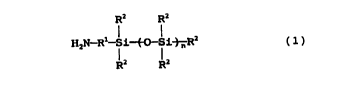
According to the invention, there is provided an ultraviolet
absorbing material comprising a reaction product of (a) an aminosilane
compound of formula (1) or the derivative thereof with (b) an ultraviolet
absorber having in its molecules a carboxyl group so as to form amide
bonds derived from the aminosilane compound or the derivative thereof,
formula (1) being represented by
CA 022~8779 1998-12-18
.
R2 R2
H2N--Rl--Si~O--Si~ R2
R2 R2
(1)
wherein R' is a C, - C10 alkylene group or a divalent group of the
formula - (CH2)m - NH - in which m is an integer of 1 - 4, R2 may be the
same or different and each are selected from the group consisting of a
hydrogen atom, a hydroxyl group, a halogen atom, a C, - ClO alkyl group
and a C, - C,O alkoxy group provided that at least one of R2 is an alkoxy
group, and n is an integer of O or greater.
An ultraviolet absorbing plate according to the invention is
produced by forming the ultraviolet absorbing layer of an ultraviolet
absorbing material having an amide bond and an Si - O bond, on a
su bstrate .
The ultraviolet absorbing material comprises preferably a
reaction product of (a) an aminosilane compound of formula (1) or the
derivative thereof with (b) an ultraviolet absorber having in its molecules
a carboxyl group so as to form amide bonds derived from the
aminosilane compound or the derivative thereof,
formula (1) being represented by
R2 R2
H2N--Rl--Si~O--Si ) R2
R2 R2 n
(1)
wherein R' is a Cl - C,O alkylene group or a divalent group of the
formula - (CH2)m - NH - in which m is an integer of 1 - 4, R2 may be the
CA 022~8779 1998-12-18
'
same or different and each are selected from the group consisting of a
hydrogen atom, a hydroxyl group, a halogen atom, a C, - C10 alkyl group
and a C1 - C10 alkoxy group provided that at least one of R2 is an alkoxy
group, and n is an integer of O or greater.
The reaction between the aminosilane compound or the
derivative and the ultraviolet absorber having in its molecule a carboxyl
group is preferably conducted in the presence of a silicone resin or is
conducted, followed by addition of a silicone resin upon completion of
the reaction.
The ultraviolet absorbing material is preferably produced by
reacting (a) an aminosilane compound of formula (1) or the derivative
thereof with (b) an ultraviolet absorber having in its molecules a
carboxyl group in the presence of a silane compound having an epoxy
group and/or a colloidal silica so as to form an amide bond derived from
the aminosilane compound or by adding a silane compound having an
epoxy group and/or a colloidal silica to a reaction product obtained by
reacting (a) an aminosilane compound of formula (1) or the derivative
thereof with (b) an ultraviolet absorber having in its molecules a
carboxyl group so as to form an amide bond derived from the
aminosilane compound,
formula (1) being represented by
R- R-
H~N--R--$i~G--$i~ R-
R- R-
(1)
wherein R' is a C1 - C10 alkylene group or a divalent group of the
CA 022~8779 1998-12-18
. .
formula - (CH2)m - NH - in which m is an integer of 1 - 4, R2 may be the
same or different and each are selected from the group consisting of a
hydrogen atom, a hydroxyl group, a halogen atom, a C1- C10 alkyl group
and a C1 - C10 alkoxy group provided that at least one of R2 is an alkoxy
group, and n is an integer of O or greater.
The substrate is preferably transparent and the ultraviolet
absorbing layer is also preferably transparent.
The substrate preferably comprises a plurality of transparent
substrates laminated one after another and one or more the ultraviolet
absorbing layers interposed therebetween.
An overcoat layer is preferably coated over the ultraviolet
absorbing layer.
The substrate has preferably a transparent electrically
conductive layer on the side where the ultraviolet absorbing layer is
disposed .
An overcoat layer is preferably disposed between the ultraviolet
absorbing layer and the transparent electrically conductive layer.
Brief Description of the Drawings
Figure 1 is a schematic cross-sectional view showing one
example of the ultraviolet absorbing layer according to the invention.
Figure 2 is a schematic cross-sectional view showing another
example of the ultraviolet absorbing layer according to the invention.
Figure 3 is a schematic cross-sectional view showing further
another example of the ultraviolet absorbing layer according to the
invention.
Figure 4 is a schematic cross-sectional view showing still another
example of the ultraviolet absorbing layer according to the invention.
CA 022~8779 1998-12-18
i
Figure 5 is a graph showing the visible ultraviolet absorbing
spectral of the ultraviolet absorbing glass produced in Example 1.
Figure 6 is a graph showing the visible ultraviolet absorbing
spectral of the ultraviolet absorbing glass produced in Example 9.
Figure 7 is a graph showing the visible ultraviolet absorbing
spectral of the ultraviolet absorbing glass produced in Example 13.
Figure 8 is a graph showing the visible ultraviolet absorbing
spectral of the ultraviolet absorbing glass produced in Example 17.
Figure 9 is a graph showing the visible ultraviolet absorbing
spectral of the ultraviolet absorbing glass produced in Example 21.
Figure 10 is a graph showing the visible ultraviolet absorbing
spectral of the ultraviolet absorbing glass produced in Example 25.
Figure 11 is a graph showing the visible ultraviolet absorbing
spectral of the ultraviolet absorbing glass produced in Comparative
Example 3.
Figure 12 is a model graph demonstratively explaining the
principle of the way of determining a change rate in ultraviolet absorbing
power.
Best Mode for Carrying out the Invention
A substrate used for the present invention may be a transparent
or opaque substrate and may be a laminate of these substrates.
There is no particular limitation imposed on the transparent
substrate. The transparent substrate may be a colorless or colored
glass, a camphor glass, a wire glass, a hot wire reflection glass, a hot
wire absorbing glass, a reinforced glass, a glass block or a colorless or
colored transparent resin. Such transparent glasses may be
polyethylene terephthalate, polyamide, polysulfone, polyethersulfone,
CA 022~8779 1998-12-18
polyetherketone, polyphenylene sulfide, polycarbonate, polyimide,
polymethylmethacrylate and polystyrene.
The term "transparent" used herein designates visible optical
transmission ranging from 3 -100 %, preferably 10 -100 %. The
substrate used for the invention has necessarily a smooth surface which
may be planner or curved at normal temperature and may be deformable
under stress and be in a vessel-like shape.
There is no particular limitation imposed on the material of the
opaque substrate. Therefore, eligible materials may be selected from
a variety of glasses such as a soda-lime glass and a borosilicate glass,
a synthetic resin, papers, woods, woven textiles, unwoven textiles, knits
and a composite material of two or more of these materials. Eligible
synthetic resins are polyethylene terephthalate, polyamide, polysulfone,
polyether sulfone, polyphenylene sulfide, polycarbonate, polyimide,
polymethyl methacrylate and polystyrene. The opaque substrate may
be white or colored.
The term "opaque" used herein means that visible light can not
be transmitted. The opaque substrate used for the present invention
has desirously an optical transmittance of less than 3 %, preferably less
than 2 % at a thickness of 2 llm. The opaque substrate used for the
invention has macroscopically a surface, which may not be flat in
microscopic view and may be curved and deformable under stress.
The ultraviolet absorbing layer has necessarily an amide bond
represented by (- CONH -) and an Si-O bond. Preferably these bonds
are attached to some bonding groups such as (a) a C, - Cs alkylene
group, (b) a divalent group represented by the formula- (CH2)m - NH -
wherein m is an integer of 1 - 4, and (c) a residue derived from (a) or
CA 022~8779 1998-12-18
'
(b)
The contents of the Si - O bond in the ultraviolet absorbing layer
should be in an amount of 1 - 50 mol, preferably 1 - 30 mol, more
preferably 1 -15 mol per mol of the amide bond.
The ultraviolet absorbing plate comprises preferably an
ultraviolet absorbing plate comprising a transparent substrate and an
ultraviolet absorbing layer which is less than 40 %, preferably less than
30 %, more preferably less than 15 % in a change rate in ultraviolet
absorbing power of an ultraviolet after the plate being subjected to 24
hour-extraction in a boiled acetone, which change rate is defined by the
following mathematical formula:
Change Rate in Ultraviolet Absorbing Power (%) =
(Absorbance prior to extraction) - (Absorbance after extraction) X 100
(Absorbance prior to extraction)
provided that the calculation is carried out using the value of
absorbance after extraction at an arbitrary wavelength region
corresponding to that at which absorbance prior to extraction is
substantially 1. Changes in ultraviolet absorbing power can be easily
observed from an ultraviolet absorbing spectrum. Take for instance, in
Figure 12 there is demonstratively shown the principle of the way of
determining change rate in ultraviolet absorbing power and it is clear
therefrom that the wavelength is about 383 nm when the absorbance
prior to extraction is 1 and the absorbance after extraction is 0.07 at the
same wavelength. Therefore, the change rate in ultraviolet absorbing
power is calculated to be 93%.
Change in ultraviolet absorbing power results from elusion of a
component derived from an ultraviolet absorbing compound (usually an
CA 022~8779 1998-12-18
i~
organic ultraviolet absorbing compound) forming an ultraviolet
absorbing layer, into acetone. However, the ultraviolet absorbing
component is substantially free from such elution if it is chemically
bonded to another component in the ultraviolet absorbing layer.
In the case of using an organic ultraviolet absorber having a
benzotriazole skeleton or a benzophenon skeleton described hereinafter
in details as an ultraviolet absorbing compound, the ultraviolet
absorbing layer thus obtained has usually the benzotriazole or
benzophenon skeleton or the structure derived therefrom. However, in
the present invention, owing to the ultraviolet absorbing compound in
the ultraviolet absorbing layer bonded through the amide bond to the
matrix, the ultraviolet absorbing layer boiled in acetone exhibits no or
slight extraction of the structure derived from the ultraviolet absorber
thereof. Therefore, the resulting ultraviolet absorbing plate is less in
change rate in ultraviolet absorbing power than the above-specified
values thereby obtaining a very little change rate.
As no particular limitation is imposed on the production method
of such a particular ultraviolet absorbing layer, any suitable methods
can be employed. One of the methods is exemplified as follows:
An aminosilane compound represented by formula (1) given
below or the derivative thereof hereinafter referred to as Component A
is reacted with an ultraviolet absorber having in its molecule a carboxyl
group referred hereinafter to as Component B so as to form an amide
bond derived from Component A thereby producing an ultraviolet
absorbing material which is coated and cured on a substrate;
formula (1) being represented by
CA 022~8779 1998-12-18
11
R2 R2
H2N Rl $i~ o si~ R2
R2 R2
(1).
In formula (1), R' is a C1 - C,O, preferably C, - Cs alkylene group
or a divalent group of the formula - (CHz)m - NH - wherein m is an
integer of 1--4. Such an alkylene group for R' may be methylene,
ethylene, trimethylene and propylene. R2 in formula (1) may be the
same or different and each are a hydrogen atom, a hydroxyl group, a C,
- C,O, preferably C, - C3 alkyl group, a C, - C,O, preferably C, - Cs
alkoxy group and a C6--C,O, preferably C6- C~, aryl group. At least one
of R2 is preferably a C, - Cs alkoxy group. Specific examples of the
alkyl groups for R2 are methyl, ethyl, propyl and i-propyl groups.
Preferred alkoxy groups for R2 are methoxy, ethoxy, propoxy and
i-propoxy groups while preferred aryl groups are phenyl and tolyl groups.
n is an integer of greater than 0, preferably between O and 3.
Preferred examples of the aminosilane compound of formula (1)
are 3-aminopropyltriethoxysilane,
3-aminopropyldiisopropylethoxysilane,
3-aminopropylmethyldiethoxysilane,
3-aminopropylpolydimethylsiloxane,
N-(2-aminoethyl)-3-aminopropyltrimethoxysilane and
3-aminopropyltris(methoxyethoxy)silane. Preferred examples of the
derivatives of the aminosilane compound are hydrolysates of the above
preferred compounds.
These aminosilane compounds and derivatives thereof may be
CA 022~8779 1998-12-18
': i
12
prepared by a conventional method.
Preferred examples of the ultraviolet absorbing material
(Component B) having in its molecule a carboxyl group are compounds
having one or more of a carboxyl group at the side chain in the molecule,
preferably organic compounds and compounds having a benzotriazole
skeleton or a benzophenon skeleton.
Preferred compounds having a benzotriazole skeleton are those
represented by the formula
HO R4
R5 -- COOH
(2) -
In formula (2), R3 is a hydrogen atom, a halogen atom and a C1 -
C,O, preferably C1 - C6 alkyl group. The halogen atom for R3 includes
fluorine, chlorine, bromine and iodine, while the alkyl group includes
methyl, ethyl, propyl, i-propyl, butyl, t-butyl and cyclohexyl groups. R3
is substituted at the 4- or 5- position of the benzotriazole skeleton, while
the halogen atom and the alkyl group are usually located at the 4-
position. R4 is a hydrogen atom or a C, - C,O, preferably C, - C6 alkyl
group. Preferred examples of the alkyl group are methyl, ethyl, propyl,
i-propyl, butyl, t-butyl and cyclohexyl groups. Rs is a C1 - C10,
preferably alkylene group or alkylidene group. Preferred examples of
the alkylene group are methylene, ethylene, trimethylene and propylene
groups, while preferred alkylidene are ethyliden and propylidene.
Specific examples of the compound of formula (2) are
CA 02258779 1998-12-18
13
3-(5-chloro-2H-benzotriazole-2-yl)-5-(1 ,1 -dimethylethyl)-4-hydroxy-
benzene propanoic acid,
3-(2H-benzotriazole-2-yl)-4hydroxy benzene ethanoic acid and
3-(5-methyl-2H-benzotriazole-2-yl)-5-(1 -methylethyl)-4-hydroxybenzene
propanoic acid.
Preferred compounds having the benzophenone skelton are
benzophenone-based compounds represented by the following
formulae;
~R7 )
( R8 m R6COOH
(3)
OH O
( R8 ~ )n
(4)
OH O OH
( R ~ ~R7 )n
(5)
OH O OH
8~6 ) COOH
(6)
CA 022~8779 1998-12-18
14
In the formulae, R7 and R8 may be the same or different and each
are a hydroxyl group or a Cl - C,0, preferably C, - C6 alkyl or alkoxy
group. n and m each are an integer ranging from 0 to 3. Specific
examples of the alkyl group are methyl, ethyl, propyl, i-propyl, butyl, t-
butyl and cyclohexyl groups. Specific examples of the alkoxy group
are methoxy, ethoxy, propoxy, i-propoxy and butoxy groups. R6 is a C,
- C,0, preferably C, - C3 alkylene or alkylidene group. Specific
examples of the alkylene group are methylene, ethylene, trimethylene
and propylene groups. Specific examples of the alkylidene groups are
ethylidene and propylidene groups.
Preferred examples of the compound having the benzophenone
skeleton include 2-hydroxy-4-methoxybenzophenone-5-carbocylic acid,
2,2'-dihydroxy-4-methoxybenzophenone-5-carboxylic acid and
4-(2-hydroxybenzoyl)-3-hydroxybenzene propanoic acid.
The ultraviolet absorber having the benzotriazole skeleton or the
benzophenone skeleton may be prepared in a conventional manner.
In the present invention, eligible ultraviolet absorbing material to
be formed into an ultraviolet absorbing layer having an amide bond and
an Si-O bond onto a substrate includes a component obtained by at
least reacting Component A and Component B so as to form an amide
bond derived from Component A. Dehydration is generally employed
for the reaction of Component A and Component B. No particular
limitation is imposed on the amount of the amide bond to be formed.
Generally, Components A and B are reacted so that the amide bond is
formed in an amount of 100 mol percent of the aminosilane of
Component A. However, less than 100 mol percent is still acceptable.
The lower limit is on the order of 50 mol percent.
_ ..
CA 022~8779 1998-12-18
- -:
The inventive ultraviolet absorbing material may contain optional
components in addition to Components A and B to an extent that an
accomplishment of the object of the invention is not hindered. The
optional components may be added during or after the reaction between
Components A and B. Hereinbelow, these optional components are
described in details.
One example of such optional components is exemplified by
silicone resins (hereinafter referred to as Component C). Component
C is preferably a reactive silicone resin having a functional group which
is reactive with the alkoxysilyl group of Component A by dehydration
and/or removing an alcohol. Preferred functional groups are an
alkoxysilyl group and a silanol group.
Such a reactive silicone resin can be readily synthesized by
subjecting alkoxysilanes or chlorosilanes to partial hydrolysis and then
condensation. Commercially available reactive resins are pure silicone
varnishes as manufactured by Okitsumo Co., Ltd. under the trade name
of "X07931-Clear", silicone resins as manufactured by Tore. Dow-
Corning Silicone Co., Ltd. under the trade name of "SR2410" and
acrylyl-modified silicone resins as manufactured by Chisso Co., Ltd.
under the trade name of "Sairacoat 1000". These silicone resins may
be put in use in the form of a solution by using a variety of solvents to an
extent that an accomplishment of the objection of the invention does not
hindered. Although not restricted, such solvents are a variety of
hydrocarbon-based solvents, ketones, ethers, esters and etheresters.
Alternatively, a variety of modified silicone resins are also eligible.
Component C may be co-existed during or after the reaction of
Component A with Component B, the former being particularly
.... ~. ,
CA 022~8779 1998-12-18
..
16
preferred .
Another example of the optional component is a variety of epoxy
silanes (hereinafter referred to as Component D) having in their
molecule an epoxy group. Preferred epoxy silanes are those
represented by the following formulae
oRl Rlo
R9--$it O--$i ) n Rl~
Rl~ Rl~
(7)
o Rl Rlo o
R--$ito--Si ) Rll / \
Rl~ Rl~
(~) -
In the formulae, R9 and R11 may be the same or different and
each are a C, - C10, preferably C, - Cs alkylene group or a divalent
group represented by the formula - R - O - R'--wherein R and R' each
are a C,--C,O, preferably C, - Cs alkylene group, R'~ may be the same
or different and each are a hydrogen atom, a hydroxyl group, a C, - C,O,
preferably C,--Cs alkyl or alkoxy group or a C6 - C,O, preferably C6- C8
aryl group provided that at least one of R'~ is an alkoxy group, preferably
a C, - Cs alkoxy group and n is an integer of greater than 0, preferably
between O and 3.
Preferred examples of the alkylene group are methylene,
trimethylene groups. Preferred examples of the alkyl group are methyl,
ethyl, propyl, i-propyl, butyl, t-butyl, pentyl, hexyl, heptyl and octyl
groups. Preferred examples of the alkoxy group are methoxy, ethoxy,
CA 022~8779 1998-12-18
' .
.~
17
propoxy, butoxy, t-butoxy, pentyloxy and hexyloxy groups. Preferred
examples of the aryl group are phenyl and tolyl groups.
Preferred examples of Component D are
3-glycidoxypropyltrimethoxysilane,
dimethoxy-3-glycidoxypropylmethylsilane,
2-(3,4-epoxycyclohexylethyl)trimethoxysilane,
dimethylethoxy-3-glycidoxypropylsilane, 1,3-bis(3-glycidopropyl)-1,3-
dimethyl-1,3-dimethoxydisiloxane and mixtures thereof.
Component D may be hydrolyzed before put in use.
Alternatively, Component D may be put in use after the epoxy group
thereof being subjected to ring-open polymerization with use cf a
suitable polymerization catalyst. Preferred polymerization catalysts
are Lewis acid catalyst such as boron trifluoride, diethylether complex,
aluminum chloride and diethyl zinc. No particular limitation is imposed
on the ring-open polymerization conditions. The polymerization
temperature may be in the range of between -80 and 130~C, preferably
-20 and 80~C and the reaction time may be selected depending upon
the conditions and mode of the reaction but usually in the range
between 10 minutes and 10 hours, preferably 1 hour and 6 hours.
Although not restricted, the solvent used for this reaction may be an
aromatic hydrocarbon such as toluene and xylene, ketones and esters.
Although Component D may be co-existed with Components A
and B during or after the reaction therebetween, the latter is preferred.
In the case of using Component D having the epoxy group having been
polymerized to open the ring thereof, it is preferably added upon the
reaction of Components A and B.
Still another example of the optional component is a polyether-
.. ... . . .. .. ..
- CA 02258779 1998-12-18
,
~ . .
18
modified polysiloxane (hereinafter referred to as Component E) and
preferably represented by the formula
Rls Rls Rls
Rl6t~--si~ Rl3--~t Rl4--~tmRl2 - -- -sito--si~ RlS
Rls Rls (9)
In the formula, R12, R13 and R14 may be the same or different and
each are a C, - C10, preferably C1 - C5 alkylene groups, R15 may be the
same or different and each are a hydrogen atom, a hydroxyl group, a C1
- C10, preferably C1 - Cs alkyl and alkoxy group or a C6- C10, preferably
C6 - C8 aryl group. Preferably at least one of R15 is a C1 - C10 alkoxy
group. m is an integer of greater than 0, preferably between 1 and 100.
n is an integer of greater than 0, preferably between 0 and 10. p is an
integer of greater than 0, preferably between 0 and 10.
The alkylene group exemplarily includes methylene, trimethylene,
and tetramethylene groups. The alkyl group exemplarily includes
methyl, ethyl, propyl, i-propyl, butyl, t-butyl, pentyl, hexyl, heptyl and
octyl groups. The alkoxy group exemplarily includes methoxy, ethoxy,
propoxy, butoxy, t-butoxy, pentyloxy and hexyloxy. The aryl group
exemplarily includes phenyl and tolyl groups.
Component E of formula (9) exemplarily includes
tetraethyleneglycol-bis(triethoxysilylethyl) ether,
polyethyleneglycol-bis(triethoxysilylethyl)ether,
polypropyleneglycol-bis(triethoxysilylethyl)ether and mixtures thereof.
Component E may be hydrolyzed before put in use.
Although Component E may be co-existed with Components A
and B during or after the reaction therebetween, the former is preferred.
CA 022~8779 1998-12-18
19
Particularly, the use of the optional components such as
Component D of epoxysilanes and Component E of polyether-modified
polysiloxanes is contributive to making the resulting ultraviolet
absorbing layer to exert excellent performances such as improved
adhesivity to a substrate without marring heat resistance and rigidity
even with the thickness increased.
The other example of the optional component is an inorganic fine
dispersion (referred hereinafter to as Component F). Although not
restricted, Component F exemplarily includes dispersions of fine
particles such as silica, alumina, titanium oxide and antimony oxide.
The fine particles are on the order of 1 -100 nm in particle size. The
dispersion medium may be water, methanol, xylene and methylethyl
ketone. Among commercial products, preferred are "LUDOX"
manufactured by Dupont and "XBA-ST" manufactured by Nissan
Chemical Co. Ltd.
Although Component F may be co-existed with Components A
and B during or after the reaction therebetween, the former is preferred.
Each of the above-mentioned optional components may be
prepared by a conventional method.
The inventive ultraviolet absorbing material to be formed into the
above-specified ultraviolet absorbing layer on a substrate may be
prepared by reacting Components A and B solely or in the presence of
the above-described optional components as needed or reacting
Components A and B and thereafter adding the optional components.
There is no particular limitation imposed on the reaction conditions as
long as an amide bond derived from Component A is formed.
Generally, Component A is mixed with Component B and optionally
CA 022~8779 1998-12-18
' ' ~,
another component in a solvent, followed by the reaction at a
temperature ranging from room temperature to 350~C, preferably 60 to
250~C, for 5 minutes to 50 hours, preferably 10 minutes to 200 hours.
The reaction may be repeated.
The solvent used for this reaction is not restricted as long as it
does not bother the accomplishment of the purpose of the invention.
However, preferred are an aromatic solvent such as toluene and xylene,
a ketone-based solvent such as cyclohexanone and a mixture thereof.
No particular limitation is imposed on the ratio between
Components A and B upon the reaction. The amount of Component B
may be selected from the ranges between 5 - 90, preferably 10 - 80
mass percent based on the total mass of Components A and B.
When the optional components are used for the reaction or
added after the reaction, no particular limitation is imposed on the
amount of each of the optional components. However, the above-
mentioned silicone resin (Component C) may be used in an amount of 5
- 300, preferably 20 - 150 mass percent based on the total mass of
Components A and B. The above-mentioned epoxysilanes
(Component D) may be used in an amount of 10--500, preferably 100 -
400 mass percent based on the total mass of Components A and B.
The above-mentioned polyehter-modified polysiloxanes (Component E)
may be used in an amount of 100 - 500, more preferably 100 - 400
mass percent based on the total mass of Components A and B. The
above-mentioned inorganic fine particles dispersions may be used in an
amount of 5 - 400, preferably 10 - 200 mass percent based on the total
mass of Components A and B.
The ultraviolet absorbing material thus obtained may be applied
~, . ,, . , .~. . . _.. ,
CA 022~8779 1998-12-18
.
21
on a substrate as a coating component immediately after completion of
the above-described reaction or after being added with the optional
components. Alternatively, the resulting coating component may be
coated after being added with another variety of optional components.
Such components exemplarily include various types of
antioxidants, a quencher, a free-radical capturing agent, an inorganic or
organic acid such as hydrochloric acid, sulfuric acid and acetic acid, a
Lewis acid such as a boron trifluoride. diethylether complex and
sodium antimony acid hexafluoride, a base such as potassium hydroxide,
sodium hydroxide, triethylamine and aniline, a catalyst having a curing
acceleration effect (to be preferably used in an amount of 0.1 - 5.0 mass
percent based on the ultraviolet absorbing material) such as an organic
metal including dibutyltin dilaurate and titanium tetraiso propoxide and a
solvent such as toluene, xylene, ethanol, isopropanol, thinner,
dirnethylformamide, cyclohexane and 1-methoxy-2-acetoxypropane.
The inventive ultraviolet absorbing layer may be formed by
coating the ultraviolet absorbing material on a substrate and then curing
the same.
The ultraviolet absorbing material prior to be coated is usually in
a liquid state. Therefore, any suitable conventional coating methods
may be employed such as spin coating, spray coating, cast coating,
blade coating, dip coating and flow coating.
The curing reaction may be conducted at a temperature between
room temperature and 250~C, preferably 60 and 250'C if using the
aforementioned catalyst having an acceleration effect. Without the
catalyst, the ultraviolet absorbing material can be cured at a
temperature between room temperature and 350~C, preferably 60 and
CA 022~8779 1998-12-18
~2
250~C. The curing reaction may be carried out usually for 10 minutes
to 5 hours.
Although not restricted, the ultraviolet absorbing layer formed on
a substrate may have a thickness in the range of usually 0.5--50 ~m.
Less than 0.5 !lm would fail to attain a suffice ultraviolet shielding effect,
while greater than 50 ,um would lead to a difficulty in coating due to
cracki n g .
By the methods and components as described above, there can
be produced an ultraviolet absorbing plate comprising an ultraviolet
absorbing layer having an Si-O bond and formed on a substrate.
The ultraviolet absorbing plate according to the invention is
capable of shielding almost completely or completely transmitting lights
in an ultraviolet region of 300 - 400 nm. More specifically, the
ultraviolet absorbing plate can shield more than 95% of transmitting
lights in the ultraviolet region. More over, more than 98% and more
than 99% of transmitting lights in an ultraviolet region can be shielded
with a preferred embodiment and more preferred embodiment of the
inventive ultraviolet absorbing plate, respectively.
In the present invention, the ultraviolet absorbing layer is
substantially transparent and preferably is almost or completely free
from a reduction in transmission in visible light ranges peculiar to a
substrate at all. The final ultraviolet absorbing plate is preferably
transparent.
The inventive ultraviolet absorbing plate comprises at least a
substrate and an ultraviolet absorbing layer but may have an overcoat
layer over the ultraviolet absorbing layer thereby providing functions
such as resistance to wear and chemicals.
CA 022~8779 1998-12-18
23
Although not restricted, preferred materials for the overcoat layer
are resins excelled in resistance to heat. Specific examples of such
resins include a silicone resin such as polyimide, polyamide,
polycarbonate, polyarylate, polyethersulfone, melamine resin, phenol
resin, epoxy resin and silicone varnish and a urea resin, among which
the silicone resins are particularly preferred. These may be used in
combination with a glass filler or an inorganic powdery material.
Eligible inorganic powdery materials are powders of ZnO, TiO2, CeO2 or
silica. Eligible silicone resins are those having inorganic fine particles
such as colloidal silica dispersed therein, partially hydrolyzed products
or partially condensed products of silanes such as alkoxysilane and
chlorosilane. Specific examples of the silicone silane which are
commercially available are "Tossguard 510" manufactured by Tohsiba
Silicone, "APZ7703" and "APZ7705" manufactured by Nihon Unicar and
polysllazane manufactured by Tohnen under the trade name of N-L110
and N-L7tO. A partially hydrolyzed product of epoxysilane is also
known as a suitable overcoat material which is excelled in resistance to
wear. Although not restricted to the method for forming the overcoat
layer and thus an suitable method can be employed, the overcoat layer
is generally formed by coating a solution of the resins or the precursor
thereof. After coating, a suitable treatment may be applied slectively
depending upon the nature of the resin. Alternatively, an overcoat
layer can be formed by applying a film of the above-described resin.
For example, a silicone varnish is added with a catalyst such as
dibutyltin dilaurate and coated over the ultraviolet absorbing layer,
followed by heat-curing at a temperature of 100 - 200~C for 5 minutes to
2 hours thereby obtaining an overcoat layer having a thickness of 1 - 20
CA 02258779 1998-12-18
,: ,
~4
~um. Alternatively, if using an acryl-melamine resin precursor, it is
coated and then cured at a temperature of 130 -190~C for 5 minutes to
2 hours thereby obtaining an overcoat layer having a thickness of 10 -
100 ,um. Further alternatively, if using a photo-curable type acryl based
resin precursor, it is coated and then placed under irradiation from a
high-tension mercury vapor lamp thereby obtaining an overcoat layer
having a thickness of 1 -10 ~um within 5 minutes.
The coating may be conducted by a known method for which
instance spin coating, spray coating, blade coating and dip coating.
Alternatively, prior to forming an overcoat layer, the coatability and
adhesivity to an ultraviolet absorbing layer can be improved by optical
surface modification and primary coating treatments.
The inventive ultraviolet absorbing plate may have over the
overcoat layer a film of metal oxides possessing heat wave reflection
and insulating functions. The film can be formed by a sputtering
method or a solgel method thereby providing the ultraviolet absorbing
plate with functions such as heat wave reflection and insulation.
The inventive ultraviolet absorbing plate is characterized by its
capability of shielding ultraviolet rays in longer wavelength regions,
compared with conventional ones. Although not restricted, the
inventive ultraviolet absorbing plate can be applied to an ultraviolet
interceptive glass, a multilayered glass, a laminated glass, a heat wave
reflective and ultraviolet interceptive glass, a heat wave and ultraviolet
absorbing glass and an anti-fogging ultraviolet absorbing glass for
windows of houses, a shopwindow, a functional glass for automobiles,
vehicles, airplanes and ships, an ultraviolet interceptive film having the
above-described ultraviolet absorbing layer formed on a film made from
CA 022~8779 1998-12-18
: .
a resin and a film for agricultural use and for a greenhouse.
Furthermore, the inventive ultraviolet absorbing plate may be those
obtained by forming the above-described ultraviolet absorbing layer
directly on the following articles instead of the above-described
substrate. The articles can be exemplified by showcases, specimen
cases, bulletin boards, architraves, glasses, sun glasses, cathode-ray
tubes, LCD (Liquid Crystal Display) such as TN (Twisted Nematic), STN
(Supertwisted Nematic), DSTN (Dual-scanned Supertwisted Nematic),
FSTN (Film-compensated Supertwisted Nematic), OMI (Optical Mode
Interference), ROCB (Reflective Optical Mode Interference), BTN
(Bystable Twisted Nematic), ECB (Electrically Controlled By- fleegence),
PALC (Plasma Addressed Liquid Crystal), G/H (Guest Host), mixed
mode, PDLC (Polymer Dispersed Liquid Crystal), IPS (In Plane
Switching), FLC (Ferroelectric Liquid Crystal) and AFLC (Anti-
ferroelectric Liquid Display), PDP (Plasma Display Panel), FED (Field
Emission Display), light-emission diode, thermochromic, electrochromic
and photochromic devices, electroluminescence devices, light fittings,
bottles and plastic containers for foods, soft drinks, liquors and
cosmetics and plastic molded articles and so on.
Furthermore, the inventive ultraviolet absorbing plate can be
used as various types of optical filters which are disposed on the outer
or inner side of the above-mentioned devices or elements to provide it
with ultraviolet absorbing capability. The inventive ultraviolet
absorbing plate may be modified to the filter by providing the above-
described ultraviolet absorbing layer directly on a substrate for various
types of LCD, an elctrochromic device, a photochromic device, a PDP
device, an FED device, a light-emitting diode, a thermochromic device
CA 022~8779 1998-i2-18
,. ,
26
and an elctroluminscence device and a substrate made of a transparent
glass or a transparent plastic film. These optical filters may be suitably
disposed anywhere in the above-mentioned devices.
In the case where the inventive ultraviolet absorbing plate is in
the form of a multi-layer constituted by two or more of transparent
substrates and having necessarily an ultraviolet absorbing transparent
plate obtained by forming an ultraviolet absorbing layer on a transparent
substrate, the embodiments of such multi-layer type plate are selective
depending on the purpose thereof. The combinations of transparent
substrates are illustrated as follows:
(1) an ultraviolet absorbing transparent plate and a transparent
plate having no ultraviolet transparent layer (transparent
su bstrate),
(2) two ultraviolet absorbing transparent plates,
(3) an ultraviolet absorbing transparent plate and a heat wave
reflective transparent plate,
(4) an ultraviolet absorbing transparent plate and an ultraviolet
reflective transparent plate,
(5) an ultraviolet absorbing transparent plate, a non-ultraviolet
absorbing transparent plate and a heat wave reflective
transparent plate,
(6) an ultraviolet absorbing transparent plate and a selected
wavelength reflective transparent plate, and
(7) an ultraviolet absorbing transparent plate and a low
emissivity transparent plate.
Needless to mention, the material of each transparent substrate
may be the same or different. In the case of using an ultraviolet
' CA 022~8779 1998-12-18
absorbing transparent plate, the ultraviolet absorbing layer formed
thereon may be exposed to the outside or built in when assembled into
the multiple layer plate, the latter being preferred.
These transparent plates may be contacted to each other or
contacted so as to have a functional material intervened therebetween.
Furthermore, the transparent plates may be disposed with a space to be
vacuumed or filled with dry air, an inactivate gas or a functional material.
The ultraviolet absorbing multi-layered plate may be prepared by
a known method except using at least one ultraviolet absorbing
transparent plate. Specific examples of the muiti-layered plate are as
follows. For example, a multi-layered glass can be easily produced by
using a spacer, a corner key, a drying agent, a sealer and a sealant in a
suitable combination, the materials of which are not limited. For
example, the spacers may be those of metals such as aluminum and
alloy or of resins such as vinyl chloride. The corner keys used in
combination with the spacer may be those of metals or resins. The
drying agents to be put into the spacer are porous materials such as
silica gel and zeolite. As a primary sealant, there may be used a
polyisobutylene sealant containing butyl rubber as a main component.
As a secondary sealant, there may be a polysulfide sealant. In the
case of a laminated glass, there may be used a polyvinylbutyral resin
and a polyurethane resin ethylene-vinyl acetate copolymer. In order to
improve resistance to penetration, a resin film of polycarbonate or
polyester may be inserted between interlayers each disposed on the
confronting surfaces of two glasses.
In the case where the inventive ultraviolet absorbing plate is an
ultraviolet absorbing electrically conductive transparent which is
CA 022~8779 1998-12-18
! .
28
produced by forming the ultraviolet absorbing layer on a transparent
substrate having a transparent electrically conductive layer thereon, the
above-described overcoat layer may be disposed between the
ultraviolet absorbing layer and the transparent electrically conductive
layer.
No particular limitation imposed on the transparent electrically
conductive layer employed for the present invention as long as it
satisfies the requirement for transparency. For example, there may be
used thin films of metal such as gold and silver and metal oxides such
as ITO (In2O3-SnO2), tin oxide, zinc oxide and vanadium oxide.
The film thickness is usually 100 to 5000 A and preferably 500 to
3000 A. The surface resistance (resistivity), which may be selected to
a suitable value depending upon the usage of the transparent
electrically conductive plate, is usually 0.5 to 500 Q/cm2, preferably 2 to
50 Q/cmZ.
There is no particular limitation imposed on the method for
forming the transparent electrically conductive layer and thus any of
known methods may be employed depending upon the types of the
metal oxides and metals used for the electrically conductive layer.
Such methods may be exemplified by a vacuum deposition method, an
ion plating method, a sputtering method and a solgel method. In any of
these methods, the electrically conductive layer may be formed at the
transparent substrate temperature ranging from 1 OO~C to 350~C.
The ultraviolet absorbing transparent electrically conductive
substrate has preferably the above-specified specified ultraviolet
absorbing layer between the transparent substrate and the transparent
electrically conductive layer. The overcoat layer may or may not be
CA 022~8779 1998-12-18
- - !
~9
disposed between the ultraviolet absorbing layer and the transparent
electrically conductive layer. The simplest structure of the ultraviolet
absorbing transparent electrically conductive substrate according to the
invention has a transparent substrate 11, an ultraviolet absorbing layer
12, an overcoat layer 13 and a transparent electrically conductive layer
14, in this order, as shown in FIG. 1.
One or more intermediate layers 15 may also be provided
between the transparent substrate 11 and the ultraviolet absorbing layer
12 as shown FIG. 2. Although there is no limitation to the function of
the intermediate layer 5, it may be an ultraviolet absorbing layer
containing inorganic oxides such as ZnO, CeOz, and TiO2 so as to
suppressing deterioration of the organic ultraviolet absorber by far
ultraviolet rays. Alternatively, the intermediate layer containing a
silane coupling agent or a surfactant may also be provided for improving
adhesion between the transparent substrate 11 and the ultraviolet
absorbing layer 12.
Furthermore, one more intermediate layers may be provided
between the ultraviolet absorbing layer 12 and the overcoat layer 13 as
shown 3. No limitation is imposed on the functions of the intermediate
layer 16. For example, an intermediate layer containing silane
coupling agents or surfactants may be provided for improving adhesion
between the overcoat layer 13 and the transparent electrically
conductive layer 14.
More over, one or more intermediate layer 15, 16 may also be
provided between the transparent substrate 11 and the ultraviolet
absorbing layer 12 and between the overcoat layer 13 and the ultraviolet
absorbing layer 12, respectively as shown in FIG. 4. Although there is
CA 022~8779 1998-12-18
no limitation to the functions of the intermediate layers 15, 16, they may
have the functions similar to those explained with FIGS. 2 and 3.
The above-described layers may be provided not only on one
surface but also both surfaces of the transparent electrically conductive
plate.
Industrial Utility of the Invention
As described above, the ultraviolet absorbing material according
to the invention has superior ultraviolet shielding effect and thus can be
used as a suitable coating material which can easily provide weathering
resistance and heat resistance properties. Due to the amide bond
between the ultraviolet absorber and the matrix, the inventive ultraviolet
absorbing material is free from bleedout and can maintain excellent
ultraviolet absorbing power even over an extended period of time.
Therefore, the ultraviolet absorbing plate according to the invention has
an amide bond and an Si-O bond in its ultraviolet absorbing layer and
can maintain excellent durability even with the high concentration of the
ultraviolet absorbing components. In addition, the inventive ultraviolet
absorbing plate is superior in resistance to weathering and resistance to
heat and can sharply shield ultraviolet rays of longer wavelength with
transmittance in visible regions being hardly reduced. The inventive
ultraviolet absorbing plate has thus an extremely superior resistance to
deterioration by ultraviolet rays and can be used as a variety of
materials and products required to have a long duration of life.
In the case of the inventive ultraviolet absorbing plate comprising
a transparent electrically conductive substrate, it has high electrical
conductivity and superior ultraviolet shielding effect. In particular, if
the ultraviolet absorbing layer is suitably selected, wavelength of 400
. .
CA 022~8779 1998-12-18
~ ~.
nm or less can be shielded very sharply. In addition, since the
transparent electrically conductive layer can be formed easily due to the
effect obtained by the overcoat layer interposed between the
transparent electrically conductive layer and the ultraviolet absorbing
layer, it becomes possible to protect an electric device produced by
using the transparent electrically conductive layer against ultraviolet
rays. By the chemical bond of the ultraviolet absorber to a polymer, the
resulting ultraviolet absorbing layer is stable even during formation of
the transparent electrically conductive layer, allowing to produce the
transparent electrically conductive plate having the ultraviolet absorbing
layer with ease. Because of the above features of the transparent
electrically conductive substrate, it is highly useful as an electrochromic
element aimed at light transmission control and display and a liquid
crystal element for display.
The present invention will be further described by way of the
following examples, which however should not be constructed in a
limiting sense. In the examples, the measurements of ultraviolet
absorbance and light transmittance to derive a change rate in ultraviolet
absorbing power was conducted by using a device manufactured by
Hitachi Seisaku-sho Co., Ltd. under a trade name U-3300 type
spectrophotometer, in a wave range of 300 to 500 nm.
Fxample 1
Synthesis of Ultraviolet Absorbing 1 ayer Havin~ Carboxyl Group
225 grams (0.46 mol) of octyl 3-(5-chloro-2H-benzotriazole-2-
yl)-5-(1,1-dimethylethyl)-4-hydroxy-benzen propanate manufactured by
Chiba-Geigy Co., Ltd. under the trade name of TINUVIN 109 were
dissolved in 700 ml acetone and then added with 600 ml 2N sodium
CA 022~8779 1998-12-18
32
hydroxide solution, followed by stirring at room temperature for 24 hours.
The resulting mixture was acidified with 650 ml 2N hydrochloric acid and
filtered to obtain an insoluble product, followed by washing it with
distilled water until the filtrate being neutralized. The resulting product
was dried in vacuum and recrystalized in toluene thereby obtaining 3-
(5-chloro-2H-benzotriazole-2-yl)-5-(1 ,1 -dimethylehtyl) -4-hydroxyy-
benzene propanoic acid referred to as Compound A hereinafter.
Preparation of Ultraviolet Absorbing Material
3 grams of 3-aminopropyltriethoxysilane were dissolved in 35
grams of xylene and added gradually with 5 grams of Compound A while
being heated at a temperature of 80~C. Upon completion of the
addition, the resulting mixture was heated up to a temperature of 130~C
and refluxed for 3 hours. The mixture was disposed still to cool down
and added with 16 grams 3-glycidopropyltrimethoxysilane thereby
obtaining an ultraviolet absorbing material (coating liquid).
13C-NMR analysis of the resulting ultraviolet absorbing material
revealed that there was a peak of carbonyl at about 173 ppm thereby
confirming the existence of an amide bond derived from the aminosilane
compound.
Preparation of Ultr~violet Absorbing Plate
The ultraviolet absorbing material obtained above was spray-
coated over a glass substrate and disposed still at room temperature for
20 minutes thereby obtaining an ultraviolet absorbing glass (ultraviolet
absorbing plate) having an ultraviolet absorbing layer of 17 !lm
th i ckn ess .
A portion of the ultraviolet absorbing layer was scraped out and
subjected to '3C-NMR analysis. It was observed that there was a peak
CA 022~8779 1998-12-18
33
of carbonyl (about 173 ppm) derived from the amide bond. 29Si-NMR
analysis also revealed the existence of the Si-O bond.
FIG. 5 shows ultraviolet visible absorbing spectrum of the
ultraviolet absorbing glass. As apparent from FIG. 5, this glass fully
shielded ultraviolets of less than 400 nm. Furthermore, this glass
performed a superior ultraviolet shielding effect over an extended period
of time.
Fxample ?
Prep~ration of Ultraviolet Absorbing Multi-layer Glass
A multi-layer glass was prepared in a conventional manner by
using the ultraviolet absorbing glass obtained in Example 1 and a
commercial soda lime glass. There were used an aluminum spacer, a
corner key, a butyl rubber, a drying agent and polysulfide all of which are
manufactured by Teipa Chemical Industry Co., Ltd. The resulting
multi-layer glass was superior in heat resistance and capable of
perfectly shielding ultraviolets over an extended period of time.
Fxample 3
A silicone resin (APZ-7705, manufactured by Nippon Unicar Co.,
Ltd.) was spray-coated over the ultraviolet absorbing layer of the
ultraviolet absorbing glass obtained in Example 1 and dried at a
temperature of 1 00~C for 20 minutes thereby forming a protection layer
having a thickness of 2 !lm.
Prep~ration of Ultraviolet Absorbin~ Transparent Flectrjcally Conductive
Substrate
ITO was formed on the protection layer by sputtering at a
substrate temperature of 250~C to form a transparent electrically
conductive layer having a layer thickness of about 3300 A and an
CA 022~8779 1998-12-18
.. .
34
electrical resistance of 7.5 Q/cm2 thereby producing a transparent
electrically conductive substrate having ultraviolet absorbing capability.
FIG. 5 shows the spectral transmittance of the transparent electrically
conductive substrate.
Fxample 4
The ultraviolet absorbing material obtained in Example 1 was
spray-coated over a stainless plate of red color and disposed still for 20
minutes, followed by heating at a temperature of 2002C for 20 minutes
thereby obtaining an ultraviolet absorbing resin plate having an
ultraviolet absorbing layer with a thickness of 17 um. The resulting
resin plate was left under radiation of ultraviolet ray and observed to be
extremely less in discoloration than a plate devoid of the coating.
Fxample 5
Preparation of Ultraviolet Absorbing Material
3 grams of 3-aminopropyltriethoxysilane were dissolved with 40
grams of xylene and gradually added with 5 gram Compound A prepared
in Example 1 while being heated at a temperature of 60~C. After
completion of the addition, the mixture was heated up to a temperature
of 130~C and refluxed for 3 hours thereby obtaining an ultraviolet
absorbing material in the form of a solution.
A peak of carbonyl at about 173 ppm derived from the amide
bond was observed by 13C-NMR analysis of the resulting solution
thereby confirming the existence of the amide bond derived from the
aminosilane compound.
Preparation of Ultr~violet Absorbing Plate
The ultraviolet absorbing material was spray-coated over a glass
plate and disposed still at room temperature for 20 minutes, followed by
CA 022~8779 1998-12-18
~5
heating at a temperature of 130~C for 30 minutes thereby producing an
ultraviolet absorbing glass (ultraviolet absorbing plate) having an
ultraviolet absorbing layer with a thickness of 10 um.
A portion of the ultraviolet absorbing layer was scraped out and
subjected to 13C-NMR analysis. It was observed that there was a peak
of carbonyl (about 173 ppm) derived from the amide bond. 29Si-NMR
analysis also revealed the existence of the Si-O bond.
The ultraviolet absorbing spectrum of the ultraviolet absorbing
glass was measured and found to perfectly shield ultraviolets similarly
to that of Example 1. Furthermore, this glass performed a superior
ultraviolet shielding effect over an extended period of time.
Fxample 6
Preparation of Ultraviolet Absorbing Multi-l~yer Glass
A multi-layer glass was prepared in a conventional manner by
using the ultraviolet absorbing glass obtained in Example 5 and a
commercial soda lime glass. There were used an aluminum spacer, a
corner key, a butyl rubber, a drying agent and polysulfide all of which are
manufactured by Teipa Chemical Industry Co., Ltd. The resulting
multi-layer glass was superior in heat resistance and capable of
perfectly shielding ultraviolets over an extended period of time.
Fxam~le 7
A silicone resin (APZ-7705, manufactured by Nippon Unicar Co.,
Ltd.) was spray-coated over the ultraviolet absorbing layer of the
ultraviolet absorbing glass obtained in Example 5 and dried at a
temperature of 1 OO~C for 20 minutes thereby forming a protection layer
having a thickness of 2 !lm.
The ultraviolet visible absorbing spectrum of the ultraviolet
CA 022~8779 1998-12-18
36
absorbing glass having a protection layer thus formed was measured
and found to shield completely ultraviolet similarly to that of Example 5.
Preparation of Ultraviolet Ahsorbing Transparent Flectrically Conductive
Substrate
ITO was formed on the protection layer by sputtering at a
substrate temperature of 250~C to form a transparent electrically
conductive layer having a layer thickness of about 3300 A and an
electrical resistance of 7.5 Q/cm2 thereby producing a transparent
electrically conductive substrate having ultraviolet absorbing capability.
Similarly to Example 5, the substrate exhibits little change in spectrum,
compared with that before sputtering.
Fxample 8
The ultraviolet absorbing material obtained in Example 5 was
spray-coated over a red polyethylene terephthalate (TET) of red color
and disposed still for 20 minutes, follcwed by heating at a temperature
of 2003C for 20 minutes thereby obtaining an ultraviolet absorbing resin
plate having an ultraviolet absorbing layer with a thickness of 17 !lm.
The resulting resin plate was left under radiation of ultraviolet ray and
found to be extremely less in discoloration than a plate devoid of the
coati ng.
Fxample 9
Preparation of Ultraviolet AbsorbinQ Material
17.7 grams of silicone varnish manufactured by Okitsumo Co.,
Ltd. under the trade name of XO-7931-CLEAR and 3 grams of 3-
aminopropyltriethoxysilane were dissolved in 35 grams of xylene and
added gradually with 5 grams of Compound A while being heated at a
temperature of 80~C. After completion of the addition, the resulting
~ ... .. ... .
CA 022~8779 1998-12-18
. ~
37
mixture was heated up to 1305C and refluxed for 3 hours thereby
obtaining an ultraviolet absorbing material in the form of a solution
(coating liquid).
Prepar~tion of Ultraviolet Absorbin~ Transparent Substrate
The ultraviolet absorbing material thus obtained was spray-
coated over a glass substrate and disposed still at room temperature for
20 minutes, followed by heating at a temperature of 2005C for 20
minutes thereby producing an ultraviolet absorbing glass having an
ultraviolet absorbing layer with a thickness of 17 !lm. A grid test was
conducted for the resulting ultraviolet absorbing glass and 50 % of peel
-off was observed.
A portion of the ultraviolet absorbing layer was scraped out and
subjected to '3C-NMR analysis. It was observed that there was a peak
of carbonyl (about 173 ppm) derived from the amide bond. 29Si-NMR
analysis also revealed the existence of the Si-O bond.
After the resulting ultraviolet absorbing glass was extracted in
boiled acetone for 24 hours, about 3% of change in ultraviolet absorbing
power was observed in accordance with the measurement using the
above-described mathematical formula (1). From this measurement, it
was found that the ultraviolet absorber was bonded to the resin through
aminosilane.
FIG. 6 shows the ultraviolet visible absorbing spectrum of the
ultraviolet absorbing glass. As apparent form FIG. 6, the glass
completely shielded ultraviolets of less than 400 nm. The result of the
pencil hardness test stipulated by JIS K5400 was 2H. The ultraviolet
absorbing glass was left in a sunshine weather meter for 1000 hours and
the change rate in ultraviolet absorbing power was still less than 2%.
CA 022~8779 1998-12-18
, .
38
Fxample 10
Preparation of Ultraviolet Absorbing Multi-layer Glass
A multi-layer glass was prepared in a conventional manner by
using the ultraviolet absorbing glass obtained in Example 9 and a
commercial soda lime glass. There were used an aluminum spacer, a
corner key, a butyl rubber, a drying agent and polysulfide all of which are
manufactured by Teipa Chemical Industry Co., Ltd. The resulting
multi-layer glass was superior in heat resistance and capable of
perfectly shielding ultraviolets over an extended period of time.
Fxample 11
A silicone resin (APZ-7705, manufactured by Nippon Unicar Co.,
Ltd.) was spray-coated over the ultraviolet absorbing layer of the
ultraviolet absorbing glass obtained in Example 9 and dried at a
temperature of 1 00~C for 20 minutes thereby forming a protection layer
having a thickness of 2 !lm.
Prepar~tion of Ultraviolet Absorbin~ Transparent Flectrically Conductive
Substrate
ITO was formed on the protection layer by sputtering at a
substrate temperature of 250~C to form a transparent electrically
conductive layer having a layer thickness of about 3300 A and an
electrical resistance of 7.5 Q/cm2 thereby producing a transparent
electrically conductive substrate having ultraviolet absorbing capability.
FIG. 6 shows the spectral transmittance of the resulting transparent
electrically conductive substrate.
Fx~mple 1?
The ultraviolet absorbing material obtained in Example 9 was
spray-coated over a unwoven textile of red color and disposed still at
~ . ~ . . . ...
CA 022~8779 1998-12-18
.39
room temperature for 20 minutes, followed by heating at a temperature
of 200~C for 20 minutes thereby obtaining an ultraviolet absorbing resin
plate having an ultraviolet absorbing layer with a thickness of 17 !lm.
The resulting resin plate was left under radiation of ultraviolet ray and
observed to be less in discoloration than a plate devoid of the coating.
Fxample 13
Preparation of Ultraviolet AbsorbinQ Materi~l
17.7 grams of silicone varnish manufactured by Okitsumo Co.,
Ltd. under the trade name of XO-7931-CLEAR and 3 grams of 3-
aminopropyltriethoxysilane were dissolved in 35 grams of xylene and
added gradually with 5 grams of Compound A while being heated at a
temperature of 80~C. After completion of the addition, the resulting
mixture was heated up to 130~C and refluxed for 3 hours, followed by
being allowed to cool down, thereby obtaining an ultraviolet absorbing
material in the form of a solution (coating liquid).
Preparation of Ultraviolet Absorbing Transparent Substrate
The ultraviolet absorbing material thus obtained was spray-
coated over a glass substrate and disposed still at room temperature for
20 minutes, followed by heating at a temperature of 200~C for 20
minutes thereby producing an ultraviolet absorbing glass having an
ultraviolet absorbing layer with a thickness of 17 ~Lm. Unlike Example 9,
a grid test revealed no peeling-off.
A portion of the ultraviolet absorbing layer was scraped out and
subjected to '3C-NMR analysis. It was observed that there was a peak
of carbonyl (about 173 ppm) derived from the amide bond. 29Si-NMR
analysis also revealed the existence of the Si-O bond. FIG. 7 shows
ultraviolet visible absorbing spectrum of the resulting glass plate. As
CA 022~8779 1998-12-18
,
apparent form FIG. 7, the glass was found to have a superior ultraviolet
shielding capability similar to that of Example 1. The ultraviolet
absorbing glass performed a superior ultraviolet shielding capability
over an extended period of time.
Fxample 14
Preparation of Ultraviolet
A multi-layer glass was prepared in a conventional manner by
using the ultraviolet absorbing glass obtained in Example 13 and a
commercial soda lime glass. There were used an aluminum spacer, a
corner key, a butyl rubber, a drying agent and polysulfide all of which are
manufactured by Teipa Chemical Industry Co., Ltd. The resulting
multi-layer glass was superior in heat resistance and capable of
perfectly shielding ultraviolets over an extended period of time.
Fxample 15
A silicone resin (APZ-7705, manufactured by Nippon Unicar Co.,
Ltd.) was spray-coated over the ultraviolet absorbing layer of the
ultraviolet absorbing glass obtained in Example 13 and dried at a
temperature of 1 OO~C for 20 minutes thereby forming a protection layer
having a thickness of 2 um.
Preparation of Ultraviolet Atlsorbin~ Transparent Flectrically Conductive
Substrate
ITO was formed on the protection layer thus formed by sputtering
at a substrate temperature of 250~C to form a transparent electrically
conductive layer having a layer thickness of about 3300 A and an
electrical resistance of 7.5 Q/cm2 thereby producing a transparent
electrically conductive substrate having ultraviolet absorbing capability.
FIG. 7 shows the spectral transmittance of the transparent electrically
CA 022~8779 1998-12-18
conductive substrate.
Fxample 16
The ultraviolet absorbing material obtained in Example 13 was
spray-coated over a acrylic plate of red color and disposed still at room
temperature for 20 minutes, followed by heating at a temperature of
200~C for 20 minutes thereby obtaining an ultraviolet absorbing resin
plate having an ultraviolet absorbing layer with a thickness of 17 ~um.
The resulting resin plate was left under radiation of ultraviolet ray and
observed to be less in discoloration than a plate devoid of the coating.
Fxample 17
Preparation of Ultraviolet ~bsorbing Material
17.7 grams of silicone varnish manufactured by Okitsumo Co.,
Ltd. under the trade name of XO-7931-CLEAR and 3 grams of 3-
aminopropyltriethoxysilane were dissolved in 35 grams of xylene and
added gradually with 5 grams of Compound A while being heated at a
temperature of 80~C. After completion of the addition, the resulting
mixture was heated up to 130~C and refluxed for 3 hours. Then the
mixture was allowed to cool down and added with 16 grams of 3-
glycidoxypropyltrimethoxysilane and 8 grams of colloidal silica
dispersions manufactured by Nissan Kagaku Co., Ltd. under the trade
name of "MIBK-ST" thereby obtaining an ultraviolet absorbing material
in the form of a solution (coating liquid).
Prepar~tion of Ultr~violet Absorbin~ Transparent Substrate
The ultraviolet absorbing material thus obtained was spray-
coated over a glass substrate and disposed still at room temperature for
20 minutes, followed by heating at a temperature of 200~C for 20
minutes thereby producing an ultraviolet absorbing glass having an
CA 022~8779 1998-12-18
4~
ultraviolet absorbing layer with a thickness of 17 um. The result of a
pencil hardness test in accordance with JIS K 5400 was 4H.
A portion of the ultraviolet absorbing layer was scraped out and
subjected to 13C-NMR analysis. It was observed that there was a peak
of carbonyl (about 173 ppm) derived from the amide bond. 29Si-NMR
analysis also revealed the existence of the Si-O bond. FIG. 8 shows-
the ultraviolet visible absorbing spectrum of the resulting glass plate.
As apparent form FIG. 8, the glass was found to have a superior
ultraviolet shielding capability similar to that of Example 1. The
ultraviolet absorbing glass performed a superior ultraviolet shielding
capability over an extended period of time.
Fxample 18
Prepar~tion of Ultraviolet Absorbing Multi-layer Glass
A multi-layer glass was prepared in a conventional manner by
using the ultraviolet absorbing glass obtained in Example 17 and a
commercial soda lime glass. There were used an aluminum spacer, a
corner key, a butyl rubber, a drying agent and polysulfide all of which are
manufactured by Teipa Chemical Industry Co., Ltd. The resulting
multi-layer glass was superior in heat resistance and capable of
perfectly shielding ultraviolets over an extended period of time.
Fxample 19
Preparation of Ultraviolet Absorbin~ Transparent Flectrically Conductive
Substrate
ITO was formed on the ultraviolet absorbing glass prepared in
Example 17 by sputtering at a substrate temperature of 250~C to form a
transparent electrically conductive layer having a layer thickness of
about 3300 A and an electrical resistance of 7.5 Q/cm2 thereby
CA 02258779 1998-12-18
. . ( -
43
producing a transparent electrically conductive substrate having
ultraviolet absorbing capability. FIG. 8 shows the spectral
transmittance of the transparent electrically conductive substrate.
Fxample ?0
Preparation of Ultraviolet Absorbing Transparent Flectrjcally Conductive
Substrate
ITO was formed on the ultraviolet absorbing glass of prepared in
Example 17 by sputtering at a substrate temperature of 250~C to form a
transparent electrically conductive layer having a layer thickness of
about 3300 A and an electrical resistance of 7.5 Q/cm2 thereby
producing a transparent electrically conductive substrate having
ultraviolet absorbing capability. The ultraviolet visible absorbing
spectrum of the resulting substrate was measured and found to have a
superior ultraviolet shielding capability similarly to that of Example 1.
Fxampl e ? 1
The ultraviolet absorbing material obtained in Example 17 was
spray-coated over a polycarbonate of red color and disposed still at
room temperature for 20 minutes, followed by heating at a temperature
of 200~C for 20 minutes thereby obtaining an ultraviolet absorbing resin
plate having an ultraviolet absorbing layer with a thickness of 17 ,um.
The resulting resin plate was left under radiation of ultraviolet ray and
found to be less in discoloration than a plate devoid of the coating.
Fxample ??
Preparation of Solution of Fpoxysilane Copolymer
200 grams of 3-glycidoxypropylmethoxysilane was dissolved in
75 grams xylene and added gradually with 4 ml boron
trifluoride diethylehter complex at room temperature. The resulting
CA 022~8779 1998-12-18
44
mixture was stirred for 4 hours and then subjected to ring-opening
polymerization thereby preparing a epoxysilane copolymer solution.
The resulting polymer was 3,300 Mw in molecular weight by polystylene
conversion .
Preparation of Ultraviolet Absorbin~ Coatin~ I iquid
17.7 grams of silicone varnish manufactured by Okitsumo Co.,
Ltd. under the trade name of XO-7931-CLEAR and 3 grams of 3-
aminopropyltriethoxysilane were dissolved in 29 grams of xylene and
added gradually with 5 grams of Compound A while being heated at a
temperature of 80~C. After completion of the addition, the resulting
mixture was heated up to 130~C and refluxed for 3 hours. The mixture
was allowed to cool down and added with 22 grams of the epoxysilane
copolymer solution obtained above thereby obtaining an ultraviolet
absorbing material in the form of a solution (coating liquid).
Preparation of Ultraviolet Absorbing Transparent Substrate
The ultraviolet absorbing material thus obtained was spray-
coated over a glass substrate and disposed still at room temperature for
20 minutes, followed by heating at a temperature of 150~C for 30
minutes thereby producing an ultraviolet absorbing glass having an
ultraviolet absorbing layer with a thickness of 15 um. The result of a
pencil hardness test in accordance with JiS K 5400 was 6H.
A portion of the ultraviolet absorbing layer was scraped out and
subjected to '3C-NMR analysis. It was observed that there was a peak
of carbonyl (about 173 ppm) derived from the amide bond. 29Si-NMR
analysis also revealed the existence of the Si-O bond. FIG. 9 shows
the ultraviolet visible absorbing spectrum of the resulting glass plate.
As apparent form FIG. 9, the glass was found to have a superior
CA 02258779 1998-12-18
ultraviolet shielding capability similar to that of Example 1. The
ultraviolet absorbing glass performed a superior ultraviolet shielding
capability over an extended period of time.
Fxample ?3
Preparation of Ultraviolet Absorbin~ Multi-layer (~lass
A multi-layer glass was prepared in a conventional manner by
using the ultraviolet absorbing glass obtained in Example 22 and a
commercial soda lime glass. There were used an aluminum spacer, a
corner key, a butyl rubber, a drying agent and polysulfide all of which are
manufactured by Teipa Chemical Industry Co., Ltd. The resulting
multi-layer glass was superior in heat resistance and capable of
perfectly shielding ultraviolets over an extended period of time.
Fx~mple ~4
A silicone resin (APZ-7705, manufactured by Nippon Unicar Co.,
Ltd.) was spray-coated over the ultraviolet absorbing layer of the
ultraviolet absorbing glass obtained in Example 22 and dried at a
temperature of 1 00~C for 20 minutes thereby forming a protection layer
having a thickness of 2 ~um.
Preparation of Ultraviolet Absorbin~ Transp~rent Flectrically Conductive
Substr~te
ITO was formed on the protection layer thus formed by sputtering
at a substrate temperature of 250~C to form a transparent electrically
conductive layer having a layer thickness of about 3300 A and an
electrical resistance of 7.5 Q/cm2 thereby producing a transparent
electrically conductive substrate having ultraviolet absorbing capability.
FIG. 9 shows the spectral transmittance of the transparent electrically
conductive substrate.
.
CA 022~8779 1998-12-18
46
Fxample 25
The ultraviolet absorbing material obtained in Example 22 was
spray-coated over a plywood of red color and disposed still at room
temperature for 20 minutes, followed by heating at a temperature of
200~C for 20 minutes thereby obtaining an ultraviolet absorbing resin
plate having an overcoated ultraviolet absorbing layer with a thickness
of 17 !lm. The resulting resin plate was left under radiation of
ultraviolet ray and observed to be less in discoloration than a plate
devoid of coating.
Fxample :?6
The ultraviolet absorbing material (coating liquid) prepared in
Example 22 was further added with 8 gram colloidal silica dispersions
manufactured by Nissan Kagaku Co., Ltd. under the trade name of
"MIBK-ST" thereby obtaining an ultraviolet absorbing material (new
coating liquid).
The new coating liquid was spray-coated over a glass substrate
and disposed still at room temperature for 20 minutes, followed by
heating at a temperature of 150~C for 30 minutes thereby obtaining a
glass plate having an ultraviolet absorbing layer with a thickness of 15
!lm. The resulting substrate was measured for ultraviolet visible
absorbing spectrum and found to have superior ultraviolet shielding
capability similarly to that of Example 1.
Fxample ~7
Preparation of Ultr~violet Absorbin~ Transparent Flectrically Conductive
Substrate
ITO was formed on the ultraviolet absorbing glass prepared in
Example 26 by sputtering at a substrate temperature of 250~C to form a
CA 022~8779 1998-12-18
,
47
transparent electrically conductive layer having a layer thickness of
about 3300 A and an electrical resistance of 7.5 Q/cm2 thereby
producing a transparent electrically conductive substrate having
ultraviolet absorbing capability. The ultraviolet visible absorbing
spectrum of the resulting substrate was measured and found to have a
superior ultraviolet shielding capability similarly to that of Example 1.
Fx~mple ~8
Prepar~tion of Ultraviolet Absorbin~ M~teri~l
3 grams of 3-aminopropyltriethoxysilane and 11 grams of the
epoxysilane copolymer solution prepared in Example 6 were dissolved
in 32 grams of xylene and added gradually with 5 grams of Compound A
while being heated at a temperature of 80~C. After completion of the
addition, the resulting mixture was heated up to 130~C and refluxed for
3 hours thereby obtaining an ultraviolet absorbing material (coating
liquid) .
Preparation of Ultraviolet Absorbin~ Transparent Substrate
The ultraviolet absorbing material thus obtained was spray-
coated over a glass substrate and disposed still at room temperature for
20 minutes, followed by heating at a temperature of 150~C for 30
minutes thereby producing an ultraviolet absorbing glass having an
ultraviolet absorbing layer with a thickness of 15 ,um. The result of a
pencil hardness test in accordance with JIS K 5400 was 5H.
A portion of the ultraviolet absorbing layer was scraped out and
subjected to 13C-NMR analysis. It was observed that there was a peak
of carbonyl (about 173 ppm) derived from the amide bond. 29Si-NMR
analysis also revealed the existence of the Si-O bond. FIG. 10 shows
the ultraviolet visible absorbing spectrum of the resulting glass plate.
CA 022~8779 1998-12-18
.
~ 48
As apparent form FIG. 10, the glass was found to have a superior
ultraviolet shielding capability similarly to that of Example 1. The
ultraviolet absorbing glass performed superior ultraviolet shielding
capability over an extended period of time.
Fxample ~9
Prepar~tion of Ultraviolet AbsorbinQ Multi-l~yer Glass
A multi-layer glass was prepared in a conventional manner by
using the ultraviolet absorbing glass obtained in Example 28 and a
commercial soda lime glass. There were used an aluminum spacer, a
corner key, a butyl rubber, a drying agent and polysulfide all of which are
manufactured by Teipa Chemical Industry Co., Ltd. The resulting
multi-layer glass was superior in heat resistance and capable of
perfectly shielding ultraviolets over an extended period of time.
Fx~ mpl e 30
A silicone resin (APZ-7705, manufactured by Nippon Unicar Co.,
Ltd.) was spray-coated over the ultraviolet absorbing layer of the
ultraviolet absorbing glass obtained in Example 28 and dried at a
temperature of 1 00~C for 20 minutes thereby forming a protection layer
having a thickness of 2 ~m.
Prepar~tion of Ultr~violet At sorbinQ Tr~nsparent Flectrically Conductive
Substrate
ITO was formed on the protection layer thus formed by sputtering
at a substrate temperature of 250~C to form a transparent electrically
conductive layer having a layer thickness of about 3300 A and an
electrical resistance of 7.5 Q/cm2 thereby producing a transparent
electrically conductive substrate having ultraviolet absorbing capability.
FIG. 10 shows the spectral transmittance of the transparent electrically
CA 02258779 1998-12-18
.
49
conductive substrate.
Fxample 31
The ultraviolet absorbing material obtained in Example 28 was
spray-coated over a ceramic of red color and disposed still at room
temperature for 20 minutes, followed by heating at a temperature of
200~C for 20 minutes thereby obtaining an ultraviolet absorbing resin -
plate having an ultraviolet absorbing layer with a thickness of 17 ~lm.
The resulting resin plate was left under radiation of ultraviolet ray and
observed to be less in discoloration than a plate devoid of coating.
Fxample 3~
The ultraviolet absorbing material (coating liquid) prepared in
Example 28 was further added with 8 gram colloidal silica dispersions
manufactured by Nissan Kagaku Co., Ltd. under the trade name of
"MIBK-ST" thereby obtaining an ultraviolet absorbing material (new
coating liquid).
The new coating liquid was spray-coated over a glass substrate
and disposed still at room temperature for 20 minutes, followed by
heating at a temperature of 150~C for 30 minutes thereby obtaining a
glass plate having an ultraviolet absorbing layer with a thickness of 15
!lm. The ultraviolet visible absorbing spectrum of the resulting
substrate was measured and found to have superior ultraviolet shielding
capability similarly to that of Example 1.
Fxample 33
Prepar~tion of Ultraviolet ~sorbing Transparent Flectrically Conductive
Substr~te
ITO was formed on the ultraviolet absorbing glass prepared in
Example 32 by sputtering at a substrate temperature of 250~C to form a
CA 022~8779 1998-12-18
'
transparent electrically conductive layer having a layer thickness of
about 3300 A and an electrical resistance of 7.5 Q/cm2 thereby
producing a transparent electrically conductive substrate having
ultraviolet absorbing capability. The ultraviolet visible absorbing
spectrum of the resulting substrate was measured and found to have a
superior ultraviolet shielding capability similarly to that of Example 1.
Comparative Fx~mple 1
22.2 grams of silicone varnish manufactured by Okitsumo Co.,
Ltd. under the trade name of XO-7931 -CLEAR was added with 10 grams
of octyl 3-(5-chloro-2H-benzotriazole-2-yl)-5-(1,1-dimethylethyl)-4-
hydroxy-benzen propanate manufactured by Chiba-Geigy Co., Ltd.
under the trade name of TINUVIN 109 and then with 20 ~LI di-n-butyltin
dilaurate, followed by dilution with 20 ml of dimethyl formamide (DMF).
The resulting mixture was spray-coated over a glass substrate. The
resulting product was dried on a hot plate at 60~C for 15 minutes and
cured by heating in an oven at 200~C for one hour thereby obtaining an
ultraviolet absorbing glass having an ultraviolet absorbing layer about
20 !lm. The resulting ultraviolet absorbing glass became whitely turbid
due to the precipitation of the ultraviolet absorber.
Comparative Fxample ~
22.2 grams of silicone varnish manufactured by Okitsumo Co.,
Ltd. under the trade name of XO-7931-CLEAR was added with 2.2
grams of octyl 3-(5-chloro-2H-benzotriazole-2-yl)-5-(1,1-dimethylethyl)-
4-hydroxy-benzen propanate manufactured by Chiba-Geigy Co., Ltd.
under the trade name of TINUVIN 109 and then with 20 ~I di-n-butyltin
dilaurate, followed by dilution with 20 ml of dimethyl formamide (DMF).
The resulting mixture was spray-coated over a glass substrate. The
CA 022~8779 1998-12-18
51
resulting product was dried on a hot plate at 60~C for 15 minutes and
cured by heating in an oven at 200~C for one hour thereby obtaining an
ultraviolet absorbing glass having an ultraviolet absorbing layer about
15 ,um. The resulting ultraviolet absorbing glass did not become
whitely turbid but were insufficient in ultraviolet shielding capability.
The resulting ultraviolet absorbing glass was subjected to
extraction in boiled acetone similarly to that of Example 9. It was found
that there was 48% decrease in weight and 95% change rate in
ultraviolet absorbing capability and that most of the ultraviolet absorber
was eluted. Furthermore, the glass was left in a sunshine weather
meter for 1000 hours. There was found 50% change rate in ultraviolet
absorbing capability and thus reduced ultraviolet shielding capability.
Comparative Fxample 3
Ultra-fine ZnO particle dispersion coatings manufactured by
Resino Color Industry Co., Ltd. under the trade name of UV-S-400 was
dip-coated over a glass substrate and cured by heating at 200~C for 20
minutes thereby forming an ultraviolet absorbing layer having a
thickness of 2 ,um. A methylene chloride solution of polyether sulfone
manufactured by ICI Co., Ltd. under the trade name of "VICTREX" PES
4100 P was spin-coated over the ultraviolet absorbing layer thus formed
thereby forming a polymer layer of about 2 ,um in thickness.
On the polymer layer was further coated the silicone varnish
used in Example 2 to form an ultraviolet absorbing layer of 15 ,um in
th i ckn ess .
Polyimide varnish manufactured by Nissan Chemical Industries
Co., Ltd. under the trade name of RN-812 was then spin-coated over the
ultraviolet absorbing layer thus formed. The resulting product was
CA 022~8779 1998-12-18
. ;
52
cured by heating in an oven at a temperature of 200~C for 30 minutes
after the solvent was dried off at a hot plate at a temperature of 60~C
thereby forming an overcoat layer of 2 ,um. Then, ITO was formed over
the overcoat layer by sputtering at a substrate temperature of not higher
than 250~C thereby obtaining a transparent electrically conductive
substrate having a transparent electrically conductive ultraviolet
shielding layer with a layer thickness of 2050 A and a surface resistance
of 9.5 Q/cm2. FIG. 11 shows the spectral transmittance of the
transparent electrically conductive substrate.