Note: Descriptions are shown in the official language in which they were submitted.
CA 02259406 1999-O1-04
WO 98/01758 PCT/L1S97/10997
DESCRIPTION
Multiplexed Active Bioloaic Array
Field of the Invention
The present invention relates generally to electronic
systems for carrying out and/or monitoring biologic reac-
tions and, more particularly, to the design, fabrication
and uses of self-addressable, self-assembling microelec-
tronic systems for carrying out and controlling multi-step
and multiplex reactions in microscopic formats.
Background of the Invention
For some time now, substantial attention has been
directed to the design, implementation and use of array
based electronic systems for carrying out and/or monitor
ing biologic reactions.
For example, it has been recognized that electronic
biosensors of various types may be used to monitor (or
measure) the progress of certain biologic reactions, and
that arrays of these sensors may be fabricated using
techniques similar to those utilized in the integrated
circuits field.
As shown in Fig. 1, a typical prior art biosensor 1
may include a biospecific immobilization surface 2 having
an immobilized affinity ligand 3 bound thereto, a trans
ducer 4 capable of sensing the occurrence of chemical
reactions which may occur between the immobilized ligand
3 and a specific analyte, and an amplification and control
unit 5 for filtering, amplifying and translating signals
' generated by the transducer 4 into various measurements
useful for monitoring the progress or occurrence of a
selected biologic reaction. Biosensors of the type
described above are discussed in some detail in Protein
Immobilization, Fundamentals & Applications, R.F. Taylor,
ed. (1991) (chapter 8); and Immobilized Affinity Liaand
Techniques, Hermanson et al. (1992) (chapter 5).
CA 02259406 1999-O1-04
WO 98/01758 PCT/US97/10997
2
The fabrication of an array of biosensors is
disclosed, for example, in U.S. Patent Application Serial
No. 07/872,582, entitled "Optical and Electrical Methods
and Apparatus for Molecule Detection" (published November
14, 1993 as International Publication No. Tn1093/22678, and
hereinafter referred to as "the Hollis et al, applica-
tion"). The Hollis et al. application is directed primar-
ily to biosensory devices comprising an array of test
sites which may be electronically addressed using a plur-
ality of conductive leads. Various types of biosensors
are described for use at the test sites, and it is sug-
gested that the test sites may be formed in a semiconduc-
tor wafer using photolithographic processing techniques.
It is further suggested that the test sites may be coupled
to associated detection circuitry via transistor switches
using row and column addressing techniques employed, for
example, in addressing dynamic random access memory (DRAM)
or active matrix liquid crystal display (AMLCD) devices.
In addition to the biosensor devices described above,
several devices capable of delivering an electrical stimu
lus (or signal) to a selected location (or test site)
within a solution or elsewhere, have been developed. As
shown in Fig. 2, these devices often include a source 6,
such as a current, voltage or power source, an electrode
7 coupled to the current source 6, a permeation layer 8
formed on one surface of the electrode 7, and a biologic
attachment layer 9 formed upon the permeation layer 8.
The permeation layer 8 provides for free transport of
small counter-ions between the electrode 7 and a solution
(not shown), and the attachment layer 9 provides for
coupling of specific binding entities.
Exemplary systems of the type described above are
disclosed in PCT Application No. PCT/US94/12270, which was
published in May 1995, and is entitled "Self-Addressable
Self-Assembling Microelectronic Systems and Devices for
Molecular Biological Analysis and Diagnostics," and PCT
Application No. PCT/US95/08570, which was published on
t
i...:.m.
CA 02259406 2002-07-22
60724-2743
3
January 26, 1996, and is entitled "Self-Addressable Self-
Assembling Microelectronic Systems and Devices for Molecular
Biological Application," (hereinafter "the Heller et al.
applications"). The Heller et al. applications describe
electronic devices which may be fabricated using
microlithographic or micromachining techniques, and
preferably include a matrix of addressable micro-locations
on a surface thereof. Further, individual micro-locations
are configured to electronically control and direct the
transport and attachment of specific binding entities (e. g.,
nucleic acids, anti-bodies, etc.) to itself. Thus, the
disclosed devices have the ability to actively carry out
controlled mufti-step and multiplex reactions in microscopic
formats. Applicable reactions include, for example, nucleic
acid hybridizations, anti-body/antigen reactions, clinical
diagnostics, and mufti-step combinational biopolymer
synthesis reactions.
Additional electronic systems for interfacing with
various solutions and/or biologic entities are disclosed in
European Patent Application No. 89-3133379.3, published
April 7, 1990 and entitled "Electrophoretic System;" U.S.
Patent No. 5,378,343, issued January 3, 1995 and entitled
"Electrode Assembly Including Iridium Based Mercury
Ultramicroelectrode Array;" U.S. Patent No. 5,314,495,
issued May 24, 1995 and entitled "Microelectronic
Interface;" and U.S. Patent No. 5,178,161, issued January
12, 1993 and entitled "Microelectronic Interface".
Those skilled in the art will appreciate, however,
that conventional electronic systems for carrying out and/or
monitoring biologic reactions (including the devices
CA 02259406 2002-07-22
60724-2743
T
3a
described in the above-referenced patents and patent
applications) are often bulky, expensive and, at times,
difficult to control. Moreover, those skilled in the art
will appreciate that, because conventional biologic systems
often utilize "off-chip" circuitry to generate and. control
the current/voltage signals which are
CA 02259406 1999-O1-04
WO 98/01758 PCT/US97/10997
4
applied to an array of test sites, it is often difficult
without the use of special equipment to precisely control
the current/voltage signals generated at particular test
sites. As for those conventional systems which do employ
"on-chip" circuitry to generate and control the current/
voltage signals which are applied to an array of test
sites, in certain cases substantial difficulties have been
encountered where it is desired to provide separate and
distinct stimuli to selected electrode sites within a
large array. One reason for this is that, when single
site stimulus specificity is desired within conventional
biosensor arrays, that need is often satisfied through the
provision of independent signal lines for each electrode
site within the array. As a result, conventional biologic
systems are often more cumbersome and expensive than is
desirable.
In view of the above-noted limitations of conven-
tional biologic systems, it is submitted that an improved
biologic system which utilizes a minimum of "off-chip"
circuitry and enables the use of large arrays of electrode
sites while providing for very precise control of the
voltages/currents delivered at a given electrode site,
would be both useful and desirable.
Summary of the Invention
The present invention is directed to the design,
implementation and use of improved electronic systems and
devices for carrying out and/or monitoring biologic
reactions.
In one innovative aspect, a biologic electrode array
in accordance with the present invention may comprise a
matrix of electrode sites, wherein each electrode site
comprises an electrode which is coupled to a respective
sample-and-hold circuit via an amplifier circuit (or
driving element). In a preferred form, the electrodes,
amplifiers and sample-and-hold circuits are integral and
form an array within a single semiconductor chip, such
t
CA 02259406 1999-O1-04
WO 98/01758 PCT/US97/10997
that each sample-and-hold circuit may be loaded with a
predefined voltage provided by a single, time-shared
digital-to-analog converter (DAC). Further, all of the
sample-and-hold circuits may be accessed through a multi-
5 plexer which may be scanned through some or all of the
electrode locations. In this embodiment, each sample-and-
hold circuit may comprise a capacitor and a transistor
switching circuit, the transistor switching circuit, when
enabled, providing electrical communication between the
capacitor and a source line formed in the matrix.
However, in alternative embodiments, the sample-and-hold
circuits may comprise some other type of memory which may
be addressed and loaded with a signal (or value) indica-
tive of a characteristic of an electrical stimulus to be
applied at an associated electrode. Such alternative
memories may include electrically erasable programmable
read only memory (EEPROM) cells used as an analog memory
(e. g., as in the non-volatile analog signal storage chips
produced by Information Storage Devices, Inc., of San
Jose, California), or other types of circuits capable of
storing control information and producing proportional
analog output values.
In another innovative aspect, a biologic electrode
array in accordance with the present invention may
comprise a single semiconductor chip having formed thereon
a memory (for example, a random access memory (RAM)), a
digital-to-analog converter (DAC} coupled to the memory,
a counter, a row decoder coupled to the counter and to the
memory, a column decoder coupled to the counter and to the
memory, and a matrix of active biologic electrode sites
coupled to the row decoder and the column decoder. In
use, binary values representing voltages to be applied at
the various electrode sites within the array are stored in
the memory using, for example, an external computer.
Then, for each address (or a selected number of addresses)
within the array a binary value is read out of the memory
and provided to the DAC which, in turn, converts the
CA 02259406 1999-O1-04
WO 98/01758 PCT/US97/10997
6
binary value to a voltage to be stored on the "hold"
capacitor at a selected address. Once all of the
addresses of the array (or the selected number of
addresses) have been scanned in this fashion, the process
may be repeated using either the same values initially
stored in the memory or new values depending upon whether
or not time variation of the voltages/currents provided at
the various electrode sites is desired. Those skilled in
the art will appreciate that the scanning process should
be repeated often enough such that the decay over time of
the stored voltages on the sample-and-hold circuits (due
to unavoidable leakage currents) does not result in an
unacceptable voltage/current errors at the electrodes. If
non-volatile sample-and-hold circuits are used (i.e., if
EEPROM or some equivalent technology is utilized), such
decays may not be significant, allowing for arbitrarily
slow update rates.
In an alternative embodiment, the memory, counter and
DAC may be disposed on one or more separate chips.
In view of the foregoing, it will be appreciated that
a biologic array in accordance with the present invention
provides for very precise control of the potentials/
currents delivered to individual electrodes within the
array, while minimizing the utilization of "off-chip"
circuitry and overall system costs. Further, by using
local sample-and-hold circuits (or other local memory
circuits) to control the level of electrical stimulus
applied to particular test sites, arrays in accordance
with the present invention may achieve a level of stimulus
specificity and electrode utilization far superior to that
achieved using most prior art systems.
In another innovative aspect, the present invention
provides for the fabrication of an entire active array
surface on a thermally-isolated membrane containing on-
board, controllable heating elements. By cycling the
temperature of the heating elements, it is possible to
T
CA 02259406 1999-O1-04
WO 98/01758 PCT/US97/10997
7
perform DNA amplification in situ, for example, by the
polymerase chain reaction.
Finally, in still another innovative aspect, the
present invention provides for the incorporation of
optical fluorescence or absorption detection circuitry
within a biologic electrode array matrix to improve coup-
ling of emitted photons into the detection electronics.
More specifically, in accordance with one embodiment of
the present invention, a biologically active electrode is
formed above a suitable optical detector such as a MOS-
photodiode structure within, for example, a CMOS circuit.
In such an embodiment, the electrode may be formed from a
substance which is at least partially transparent, or the
electrode may be formed in such a fashion that it permits
the passage of light through its body to an underlying
photodetector.
In view of the foregoing, it is an object of the
present invention to provide an improved biologic
electrode array for carrying out and controlling multi
step and multiplex reactions in microscopic formats.
It is another object of the present invention to
provide an improved biologic electrode array which is
compact and minimizes the utilization of off-chip control
circuitry, even for large numbers of electrodes.
It is another object of the present invention to
provide an improved biologic electrode site which includes
a sample-and-hold circuit, and which may be fabricated
using conventional CMOS semiconductor fabrication
techniques.
It is still another object of the present invention
to provide an improved biologic electrode array which
includes heating elements for enhancing the progression of
reactions such as DNA amplification in situ.
It is still another object of the present invention
to provide an improved biologic array which includes a
plurality of optical detectors formed beneath selected
electrode sites.
CA 02259406 1999-O1-04
WO 98/U1758 PCTIUS97/10997
8
Brief Description of the Drawings
Fig. 1 is an illustration of a prior art passive
biologic system.
Fig. 2 is an illustration of a prior art active
biologic system.
Fig. 3 is an illustration of a biologic array in
accordance with one form of the present invention.
Fig. 4(a) is an illustration of a biologic electrode
site in accordance with one form of the present invention.
Fig. 4(b) is a circuit diagram showing in more detail
one of the switching circuits and the amplifier circuit of
the biologic electrode site illustrated in Fig. 4(a).
Fig. 4(c) illustrates how those portions of the
electrode site illustrated in Fig. 4(b) might be
fabricated using CMOS circuitry.
Fig. 5 is an illustration of a biologic electrode
site which includes circuitry for monitoring an electrical
characteristic of an electrode located at the site.
Fig. 6(a) illustrates the fabrication of a combined
thermally isolated membrane and biologic electrode array,
wherein the biologic electrode array is etched onto a back
side surface of a silicon substrate.
Fig. 6(b) illustrates the attachment of a low-ther
mal-conductivity chamber to the combined thermally
isolated membrane and biologic electrode array shown in
Fig. 6(a).
Fig. 7 illustrates a biologic electrode site
including an optical detector in accordance with the
present invention.
Fig. 8(a} is a top view of a punctuated, partially
transparent electrode in accordance with one form of the
present invention.
Fig. 8(b) is a top view of an alternative embodiment
of a partially transparent electrode in accordance with
the present invention.
t
CA 02259406 1999-O1-04
WO 98/01758 PCT/US97/10997
9
Detailed Description of Preferred Embodiments
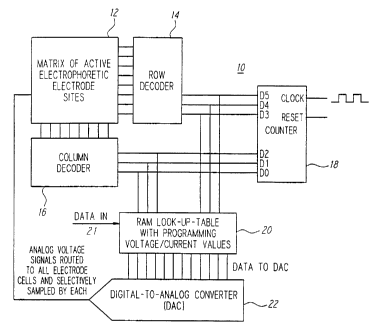
Turning now to the drawings, as shown in Fig. 3, a
biologic array 10 in accordance with one preferred form of
the present invention may comprise a matrix of active
biologic electrode sites 12, a row decoder 14, a column
decoder 16, a counter 18, a random access memory (RAM) 20
acting as a look-up table, and a digital-to-analog con-
verter (DAC) 22. In a preferred form, each of the above
listed elements may be disposed on a single semiconductor
chip, and the entire array 10 may be fabricated using
conventional CMOS semiconductor fabrication techniques.
Further, in the presently preferred form a computer (not
shown) may be used to load data, as needed, into the RAM
via, for example, a data input port 21.
15 Turning now also to Fig. 4(a), each biologic elec-
trode site 24, which makes up the matrix of biologic elec-
trodes 12, may comprise a sample-and-hold circuit 26, an
amplifier 28 and an electrode 30. In one preferred form,
the sample-and-hold circuit 26 may comprise a capacitor 32
20 and two transistor switches 34 and 36. The switches 34
and 36 are connected in series and, when closed, provide
electrical communication between a voltage source line 37
(coupled to the DAC 22) and the capacitor 32. The
switches 34 and 36 are coupled, respectively, to a desig-
nated row select line 38 and column select line 40 formed
within the matrix 12.
As shown in Figs. 4(b) and 4(c), each row select line
38 and each column select line 40 may comprise, for
example, a positive control line (+ control line) 41 and
a negative control line (- control line) 43, and each
switch 34 or 36 may comprise a CMOS transmission gate,
i.e., a PMOS FET 45 having a gate region 47 coupled to the
negative control line 43 and a NMOS FET 49 having a gate
region 51 coupled to the positive control line 41. In
addition, the amplifier circuit (or driving element) 28
may comprise a PMOS current source 53.
CA 02259406 1999-O1-04
WO 98/0I758 PCT/US97/10997
In an alternative embodiment, a single switch, such
as that described above, may be controlled by a two input
logic gate (e. g., an AND or NAND gate) with complementary
outputs (e.g., a + control line and - control Iine), and
5 may be used to selectively connect the capacitor 32 to the
voltage source line 37. In such an embodiment, the logic
gate would respond to a coincidence of signals on the row
and column select lines 38 and 40, respectively. Further,
it may be noted that in some instances a two transistor
10 transmission gate will not be needed, and a single MOS
transistor can be used as a switch. In such a case, the
logic gate need only provide a single output to the
switch.
The design, fabrication and function of counters, row
decoders, column decoders, digital-to-analog converters,
and random access memories are well known in the art and,
thus, the structure and operation of those elements are
not discussed in detail herein. Rather, a general
description of the function of the biologic electrode
array 10 is provided below.
In use, binary values representing voltages to be
applied at the various electrode sites 24 within the
matrix 12 are stored in the RAM 20 (or other suitable
memory device) using, for example, an external computer.
Then, for each address (or a selected number of addresses)
within the matrix 12 a binary value is read out of the RAM
20 and provided to the DAC 22 which, in turn, converts the
binary value to a voltage to be stored on the capacitor 32
located at the selected site address. An output amplifier
28 is coupled between the capacitor 32 and the electrode
30 and provides an amplified stimulus signal to the elec-
trode 30. The output amplifier 28 may comprise a voltage
amplifier and/or buffer and may thus amplify the voltage
on the capacitor 32 and provide an amplified voltage to
the electrode 30. Alternatively, the output amplifier 28
may comprise a current output amplifier (for example, a
transconductance amplifier) and provide a current signal
t
CA 02259406 1999-O1-04
WO 98/01758 PCT/US97/10997
11
to the electrode 30. Once all of the addresses of the
matrix (or the selected number of addresses) have been
scanned in this fashion, the process may be repeated using
either the same values initially stored in the RAM 20 or
new values, depending upon whether or not time variation
of the voltages/ currents provided at the various elec-
trode sites is desired. Those skilled in the art will
appreciate that the scanning process should be repeated
often enough such that the decay over time of the stored
voltages on the capacitors 32 (due to unavoidable leakage
currents) does not result in an unacceptable voltage/
current error at the electrodes 30.
In equivalent and alternative forms, the counter 18,
RAM 2 0 , and DAC 22 may be placed on or of f of the chip
comprising the electrophoretic electrode array, as a
matter of design choice, and if desired, some other type
of circuit (for example, a simple counter or shift
register) may be used to control the sequential loading of
the sample-and-hold circuits 26 located at the respective
electrode sites 24.
Turning now also to Fig. 5, for some applications it
may be desirable to provide for monitoring of the condi-
tion (or electrical characteristics) of one or more of the
electrodes 30 within the matrix 12. In this case, it is
assumed that if the electrode is driven with a known cur-
rent, the voltage that develops is sensed, or, if the
electrode is driven with a known voltage, the current that
flows is sensed. To allow monitoring of the condition of
a given electrode 30 a voltage sense amplifier 42 may be
coupled to the electrode 30 and to a secondary multiplex-
ing bus or output pin (not shown). The voltage sense
amplifier 42 provides an indication of the voltage at the
electrode 30 relative to an electrical ground (not shown)
for the entire array or relative to a selected reference
electrode (not shown) on the array. The voltage of the
reference electrode may, in some instances, also be the
ground used for the array. It should be noted that the
CA 02259406 1999-O1-04
WO 98/01758 PCT/US97/10997
12
output of the sense amplifiers 42 for the electrode sites
24 in the array may also be multiplexed onto a common
sense signal line, and that the signals provided to the
common sense signal line may be de-multiplexed using
conventional circuitry, such as a sample-and-hold circuit
(not shown) and an analog-to-digital converter (not
shown). The common sense signal line may be separate from
the common signal line (i.e., the voltage source line 37),
or it may be same line, in which case, it would be time
shared, serving for some selected periods of time to
provide charging signals to the capacitors 32 of the
electrode sites 24, and serving for other periods of time
as a carrier for sense signals generated at the electrode
sites 24.
In the case where the electrodes 30 are driven by
voltage amplifiers 28 and the current that flows through
the electrode 30 is to be sensed, a sense resistor (not
shown) may be connected between the output of the voltage
amplifier 28 and the electrode 30, and two inputs of a
differential amplifier circuit (not shown) may be con-
nected across the sense resistor. In such an embodiment,
the signal generated at the output of the differential
amplifier will be proportional to the current flowing
through the electrode 30.
As explained to some extent above, while the
embodiments illustrated in Figs. 4(a) and 5 employ two
switches 34 and 36 connected in series to control the
loading of the capacitor 32 (one switch being controlled
by each of the row and column lines, respectively) those
skilled in the art will appreciate that the switching
function may be implemented in any of a number of ways .
For example, it would be considered equivalent to replace
the switches 34 and 36, shown in Figs. 4 (a) and 5, with
CMOS transmission gates or a combination of an AND gate
and a switch.
Turning again to Fig. 4(c), in a preferred form the
biologic array 10 may be fabricated using a CMOS or other
t
CA 02259406 1999-O1-04
WO 98/01758 PCT/LTS97I10997
13
active circuit process. Moreover, those skilled in the
art will appreciate that completely fabricated CMOS
circuitry embodying some or all of the above-described
functions may be post-processed to form the complete
active biologic electrode array 10 described above. For
example, as illustrated in Fig. 6, the biologic electrodes
30 may be disposed atop the underlying CMOS circuitry and
then protected with an overlapping passivation layer 44.
Further, openings in the passivation layer 44 may be
fabricated to expose the active regions of the biologic
electrodes 30 as well as any required peripheral inter-
connection sites, e.g., bond-pads (not shown). In such an
embodiment, the electrodes 30 may be fabricated from elec-
trochemically suitable materials, such as gold, iridium or
platinum, and may be deposited and patterned using conven-
tional thin-film deposition techniques. The passivation
layer 44 may comprise, for example, plasma-deposited
silicon nitride and/or silicon carbide, and openings in
the passivation layer 44 may be formed using conventional
microfabrication techniques such as plasma etching.
Finally, if biomolecules are to be bound on or near the
surface of the electrodes 30, coupling agents and/or
intermediate layers (shown in Fig. 7) may be used.
Turning now to Figs. 6(a) and 6(b), in another pre
ferred form the entire active surface of the biologic
array 10 may be formed on a thermally-isolated membrane 46
containing one or more on-board, controllable heating
elements (not shown). The thermally-isolated membrane can
be formed using micromachining techniques well-known in
the art. For example, the back-side of the completed CMOS
waver containing the biologic array circuitry and elec-
trodes can be coated with a suitable etch mask (e. g.,
silicon nitride). The silicon nitride is patterned using
standard techniques to form openings where the membrane is
to be formed. The membranes are formed by submerging the
wafer in an etching solution (e. g., tetramethylammononium
hydroxide loaded with dissolved silicon, as described in
i a
CA 02259406 2002-07-22
60724-2743
14
Klassen, et al., "Micromachined Thermally Isolated.
Circuits," Proceedings of the Solid-State Sensor a.nd
Actuator Workshop, Hilton Head, South Carolina, June 3-6,
1996, pp. 127-131). The membrane can thus be temperature
cycled to allow DNA amplification in situ. Further,
controllable heating of the membrane may be accomplished
through the use of an array of resistors or appropriately
biased MOSFETS (metal oxide semiconductor field effect
transistors) distributed throughout the membrane area.
Thus, if a solution 48 (shown in Fig. 7(b)) overlying the
array 10 is provided with DNA and suitable chemicals to
carry out a polymerase chain reaction (PCR) to amplify the
DNA, cycling the temperature of the membrane will allow the
desired amplification. If thermal feedback is desired, the
temperature of the membrane may be readily determined. For
example, the temperature coefficient of resistance; of the
heater resistors or the forward voltage of diodes
incorporated into the membrane may be utilized to provide an
indication of the solution temperature. Finally, once the
DNA contained within the solution 48 is amplified,
appropriate chemicals may be injected into the chamber 60 to
effect one or more desired analysis steps. Examples of such
chemicals are restriction enzymes, fluorescent labels and
intercalcators, etc.
An exemplary micromachined, membrane-based DNA
amplification system has been demonstrated by Northrup, et
al. (see Northrup et al., "DNA Amplification with a
Microfabricated Reaction Chamber," Proceedings of
Transducers '93, the 7th International Conference on Solid
State Sensors and Actuators, Yokohama, Japan, June 7-10,
1993, pp. 924-926 and, thus, the specific structure and
I is: ~'.
CA 02259406 2002-07-22
60724-2743
14a
operation of the membrane-based DNA amplification system is
not discussed herein in detail. However, it should be noted
that the Northrup et al. system provides merely for thermal
cycling, and has no analysis or biologic electrode control
capabilities. Thus, it is believed that those skilled in
CA 02259406 1999-O1-04
WO 98/01758 PCTlUS97/10997
the art will find a biologic array in accordance with
present invention to be highly advantageous, as such an
array allows for in situ DNA amplification and subsequent
analysis using a single device.
5 Turning now to Fig. 7, for some applications, it may
be desirable to incorporate optical fluorescence or trans-
mittance detection circuitry directly into the electrode
matrix 12 to improve coupling of emitted or transmitted
photons into any provided detection electronics. In the
10 case of fluorescence detection, the entire array would be
illuminated with light at wavelengths) known to excite
fluorescence in the fluorescently labeled biomolecules
such as DNA or intercalators between DNA strands. This
light would be detected by the optical detection means
15 located at each site. In the case of transmittance detec-
tion, the entire array would be illuminated with light at
wavelength (s) known to be attenuated by the presence of
the biomolecules of interest (i.e., the light at those
wavelengths is absorbed by the biomolecules). The
presence of the biomolecules of interest at a given elec-
trode site would be detected by an attenuation of the
light sensed by the optical detector local to that site.
This approach can greatly improve the signal-to-noise
ratio (SNR) over the use of an imaging camera remote to
the biologic array 10. In essence, this involves combin-
ing a biologically active electrode (with or without
active multiplexing circuitry) above a suitable optical
detector 50 such as a MOS-photodiode or a charge-coupled
device (CCD) structure. In such an embodiment, it may be
desirable to utilize transparent electrodes, such as those
formed from indium tin oxide (ITO), or it may be desirable
to utilize a slitted or punctuated electrode structure,
such as that shown in Figs. 8(a) and 8(b). By providing
orifices 54 (as shown in Fig. 8(a)) or troughs 56 (shown
in Fig. 8(b)) through the surface of the electrode 52 it
is possible to allow the passage of light through the
electrode 52 to the optical detector 50. Those skilled in
CA 02259406 1999-O1-04
WO 98/01758 PCT/LTS97/10997
16
the art will appreciate that by eliminating the need for
an external camera and retaining the ability to perform
biologically-controlled hybridizations (or other molecular
interactions), the overall cost of a complete analysis
system can be greatly reduced.
While the invention of the subject application may
take several alternative and equivalent forms, specific
examples thereof have been shown in the drawings and are
herein described in detail. It should be understood,
however, that the invention is not to be limited to the
particular forms or methods disclosed, but to the con-
trary, the invention is to cover all modifications,
equivalents, and alternatives falling within the spirit
and scope of the appended claims.
t