Note: Descriptions are shown in the official language in which they were submitted.
CA 022~9641 1999-01-06
WO 98/o1ss6 pcTluss7ll3lo4
M~CROPHONE NOISE REJECT~ON SYSTEM
This application claims the benefit of U.S. Provisional Application
No. 60/015,861, filed July 8, 1996.
The present invention relates to noise rejection systems, and more
5 particularly to a system for rejecting repetitive noise from an information signal.
BACKGROUND OF TIlE INVENTION
Communication systems are often subject to repetitive background
noise. For example, automobile muffler systems, machines on a production
10 floor, engines in a vehicle, boat and airplane, or any other source of repetitiv
noise can interfere with an acoustic or other pick-up, such as a microphone,
hand set of a telephone, hydrophone, vibration sensor, or electronic transducer
located near the noise source. In particular, microphones in emergency vehicle
communication systems associated with police cals, fire trucks and ambulances
15 pick-up not only a user's voice, but also a repetiti~ e background noise generated
by the emergency vehicle siren. This repetitive background noise can often
overpower a user's voice so that a user's message is difficult to understand. Ifvoice-activated communication systems are employed, background noise
increases the difficulty in recognizing voice commands for automatically turning20 on and off the communication system.
Microphone noise rejection systems have been developed to
minimize the level of background noise relative to the level of the desired
information or voice signal. Such noise rejection systems typically comprise
dual microphones in which a first microphone primarily receives background
25 noise and a second microphone primarily receives both background noise and aninformation or voice signal. The noise signal is then added to or subtracted from
the information signal in order to cancel noise frc m the information signal. For
example, U.S. Pat. No. 5,381,473 issued to An~lrea shows a noise-rejection system
that uses two microphones to generate res~c.-ively a noise signal and a source
SUBSTITUTE SHEET (RULE 26)
CA 022~9641 1999-01-06
W O 98/01956 PCT~US97/13104
signal. The noise and source signals are supplied to a differential amplifier tocancel noise from the source signal. The phases of the noise and source signals
must be tightly controlled relative to each other in order to successfully remove
unwanted noise from the source signal. Unfortunately, this tight phase control
5 is difficult to achieve because the phases of the noise and source signals areextremely sensitive to slight variation in the length of each signal path from the
signa~ source to the noise rejection processing circuitry. The present inventionovercomes the phase control problem by an appalatus and method which is
independent of the path length of the signals from the signal source to the noise
10 rejection circuitry.
It is therefore an object of the present invention to substantially
e~iminate repetitive background noise from an information or voice signal
without the disadvantages inherent in the prior approaches to noise rejection.
SUMMARY OF THE INVENTION
The present invention resides in a method of rejecting repetitive
noise. A characteristic frequency and associated period of a repetitive noise
signal is identified from a first source. An information signal having an
information component and a repetitive noise component is received from a
second source that is distinct frorn the first source. The information signal isdelayed for a selected period of time based on the characteristic frequency of the
repetitive noise signal to form a phase-shifted or delayed information signal.
The delayed information signal is processed with a non-delayed information
signal to form a processed information signal in which the information
component is substantial and the noise component is negligible.
The present invention also resides in an apparatus for removing
repetitive background noise. The noise rejection apparatus comprises a first
input interface for receiving a repetitive noise signal that has a characteristic
frequency and associated period. A second input interface distinct from the first
input interface is provided for receiving an illforlnation signal having an
SUBSTITUTE SHEET (RULE 26)
CA 022~9641 1999-01-06
W O98/01956 PCTAUS97/13104
information component and a repetitive noise component. A means for
delaying the information signal for a selected period of time based on the
characteristic frequency of the repetitive noise signal forms a phase-shifted ordelayed information signal. A means for processing the delayed information
5 signal with a non-delayed information signal is plovided to form a processed
information signal in which the information component is substantial and the
noise component is negligible.
One advantage of the present invention is that the noise rejection
system does not suffer from the phase alignment problems inherent in adding or
10 subtracting information and noise signals in orde~ to remove the noise
component from the information signal.
Other objects and advantages of the present invention will become
apparent in view of the following detailed description and accompanying
drawings.
BRIEF D~!~CI~TPTION OF THE DRAWINGS
FIG. 1 illustrates in block diagram form a digital embodiment of the
microphone noise rejection system in accordance with the present invention.
FIG. 2 is a flow chart of the procedural steps taken by the
20 microprocessor of FIG. 1 for generating a processed information signal in which a
noise component is negligible.
FIG. 3 schematically illustrates an analog embodiment of the
microphone noise rejection system in accordance with the present invention.
D~:TAILED DESCRIPTION OF THE PREFERRED EMBODIMl~TS
FIG. 1 schematically illustrates a digital implementation of a noise
rejection system 10 for substantially eliminating repetitive background noise
from a microphone communication system. The noise rejection system 10
comprises an information signal interface, such as a first microphone 12, for
SlJt~S 111 UTE SHEET (RULE 26)
CA 022~9641 1999-01-06
W O 98/01956 PCTAUS97/13104
receiving an analog information or voice signal. The first microphone 12 is
coupled to an analog-to-digital converter (A/D converter) 14 at an input 16. TheAlD converter has a data output at 18 that is coupled via a data/address bus 20 to
a processor, such as microprocessor 22, having a data input at 24. The
5 rnicroprocessor 22 has a bus interface at 26 that is coupled to an external memory
module 28 at a bus interface at 30. The memory nlodule 28 may include read
only memory (ROM) and random access memory (RAM) for aiding the
microprocessor 22 in storing and processing digital information. Alternatively,
the external memory module 28 may be substituted by internal memory within
the microprocessor 22. The memory module 28 has a bus interface at 32 that is
coupled via the bus 20 to a D/A converter 34 at a data input 36. The D/A
converter 34 includes a data output 38 that is coupled to a transmitter interface
40. The A/D converter 14 and the D/A converter 34 may alternatively be
accessed as a decoded address in conjunction with single enable/disable lines.
The noise rejection system further includes an input interface 41
(shown in dashed lines) or means for identifying the characteristic frequency ofone or more noise sources. The input interface may be embodied by any
combination of standard components which cooperate to identify the
characteristic frequency of a noise source. An example of an input interface 41 (as
20 s~own in the embodiment of FIG. 1) includes means for sensing the
characteristic frequency when the characteristic frequency varies with time.
Specifically, the input interface 41 includes a second microphone 45 for receiving
an audi~le siren signal which is emitted by a repetitive noise generator such assiren or loudspeaker 44 that is driven by a siren driver 42. The second
2s microphone 45 must be located at a sufficient distance from the first microphone
~ so that any voice signal pick-up by the second microphone 45 is negligible.
Furthermore, the second microphone 45 may be lc-cated at the noise source or at
a remote location thererlom so long as the second microphone is close enough to
the noise source in order to pick up for identificat~on the characteristic frequency
SlJ~:j 111 UTE SHEET (RULE 26)
CA 02259641 1999-01-06
W O 98/01956 PCTrUS97/13104
of the noise signal.
The input interface 41 further includes a conditioning circuit 46
having inputs coupled to the siren driver 42 and the second microphone 45, and
an output coupled to the microprocessor 22 for "cleaning-up" the digital siren
5 signal received directly from the siren driver 42 or an analog siren signal
received from the second microphone 45. The conditioning circuit 46 may
indude or be associated with a switch controlled either manually or by the
microprocessor 22 for selecting either the analog ~iren signal received from thesecond microphone 45 or the digital siren signal received directly from the siren
10 driver 42. An A/D converter may be provided in association with the second
microphone 45 or the conditioning circuit 46 for (onverting the analog noise
signal received by the second microphone 45 befo] c further processing by the
mi~oprocessor 22.
Preferably, the siren signal is in the fl)rm of a square wave. The
15 characteristic frequency may be selected to be the fundamental frequency or aharmonic of the siren signal. Further, the siren signal may have a characteristic
frequency that exhibits a periodicity. For example. the siren frequency may
slowly increase and decrease in a recurring manner.
The operation of the digital implementation of the noise rejection
20 system 10 will now be explained in detail. The microphone 12 receives an audio
information signal having an information component, such as a user's voice
signal, and a repetitive noise component originating from the siren driver 42 via
the loudspeaker 44. The microphone 12 continuously generates an analog
electrical information signal which is input to the A/D converter 14 at 16. The
25 A/D converter transforms the analog information signal into digital form. Thernicroprocessor 22 processes the digital information after accessing the D/A
converter and retrieving the digital information signal via the bus 20.
Simultaneously with the proces~ing of the information signal, the
microprocessor 22 directly receives from the inpul interface 41 a digital repetitive
SU~S 111 ~TE SHEET (RULE 26)
CA 022~9641 1999-01-06
W O 98/01956 PCTAUS97/13104
noise signal via the conditioning circuit 46 which "cleans-up" the digital noisesignal for digital processing by the microprocessor 22. The microprocessor 22
determines the period associated with the current characteristic frequency of the
digital noise signal for purposes to be explained shortly. The microprocessor may
5 also be employed to effect bandwidth spectrum balance, alter intensity ratios
among the received signals and improve intelligibility of the signals or any other
desired signal characteristics.
The digital information signal retrieved by the microprocessor 22 is
then stored either in memory within the microprocessor 22, or within the
10 external memory module 28 for a predetermined delay time that is a function of
the period associated with the current characteristlc frequency of the digital noise
signal received by the microprocessor at input 43. The delay time may range
from a portion to a few periods associated with the characteristic frequency of the
repetitive noise signal, and preferably corresponds to one full period of the noise
15 signal. The characteristic frequency, as mentioned above, may slowly change
over time but may be treated generally as a constant within the brief delay times
associated with a few periods of the noise signal.
A digital information signal is stored or delayed in the memory
module 28 which acts as a first-in-first-out (FIFO) device. After the delay time20 elapses, the microprocessor 22 accesses the memory module 28 and retrieves the
delayed digital information signal via the data/address bus 20. The
microprocessor 22 then digitally subtracts the level of the delayed information
signal from that of a non-delayed or current information signal to form a
processed information signal in which the level of the information component
25 is substantial and the level of the noise component is negligible. Alternatively,
the microprocessor 22 may digitally subtract the level of the non-delayed or
current information signal from that of the delayed information signal to form
the processed information signal. The effect of the above processing is to cancel
the repetitive portion (noise component) c~ the il-formation signal while
SUBSTITUTESHEET(RULE26)
.
CA 022~9641 1999-01-06
WO 9B/019S6 PCI/US97/13104
substantially maintaining the non-repetitive component (information or voice
signals) received by the microphone 12.
Alternatively, the predetermined delay time may correspond to an
odd number of half periods of the repetitive noise signal, and preferably
corresponds to one half period of the noise signal. In this instance, after the
delay time elapses, the microprocessor 22 accesses the memory module 28 and
retrieves the delayed digital information signal ~~ia the data/address bus 20. The
microprocessor 22 then digitally adds the level of the delayed information signal
to that of the non-delayed or current information signal to form the processed
information signal. The effect of the above proce~sing similarly results in the
cancellation of the repetitive portion (noise com~onent) of the information
signal while substantially maintaining the non-r~petitive component
(information or voice signals) received by the microphone 12.
Another embodiment of the input interface or identifying means
may include a means for loading and supplying a predetermined characteristic
frequency (not shown) to the microprocessor 22 ~hen the characteristic
fre~uency is at a constant and known value. Because the characteristic frequencyis predetermined, there is no need for sensing circuitry such as the second
microphone 45 shown in FIG. 1.
The noise rejection system of the present invention improves upon
the phase alignment difficulties inherent in noise rejection systems which add or
subtract information signals with noise signals. ~ith prior noise rejection
systems that mathematically manipulate a noise ~iignal with an information
signal, it is difficult to establish a reference by whi~h to precisely control the
phase relationship between the signals. The present invention, on the other
hand, avoids this prior problem by establishing the information signal with the
noise as a "reference" among the mathematically manipulated signals. In the
present invention as described above, the noise signal is not mathematically
manipulated with an information signal. Rather, the noise signal determines
SUBSTITUTE SHEET (RULE 26)
, . . . . .
CA 022~9641 1999-01-06
W O 98/01956 PCT~US97/13104
the precise delay or phase shift to app}y to the information signal for forming a
delayed signal relative to the "reference" or current information signal. Once the
phase shift is determined, the precisely delayed information signal can be
mathematically manipulated with the "reference" or non-delayed information
signal in order to cancel noise therefrom.
FIG. 2 illustrates in flow chart form an example of the procedural
steps that may be taken by the microprocessor 22 of FIG. 1 for generating the
processed information signal. The microprocessor 22 is initialized for operation(step 100~. The predetermined period for sampling the information signal is
then set (step 102). The desired sampling period corresponds to the selected
characteristic frequency of the repetitive noise signal. For example, the sampling
period may co~res~ond to either a half period, full period, or multiple thereof of
the repetitive noise signal, as was explained with respect to the operation of FIG.
1. The microprocessor 22 next determines if the sampling period can begin (step
104). If the previous sampling period has not yet finished (decision at step 104 is
"No"), the microprocessor 22 waits until the previous sampling period has
finished. Then the microprocessor 22 samples the digital information signal
received from the A/D converter 14 (step 106). Each sample of the digital
information is stored at a unique location in memory within the microprocessor
22 or in the external memory module 28 as referenced by a pointer (step 108).
The microprocessor 22 next retrieves offset data associated with the delayed
information signal which was sampled and delayed for a predetermined length
of time corresponding to, for example, either a half or full period associated with
the characteristic frequency of the noise signal (step 110). If the desired offset or
delay time is a full period of the noise signal, the offset or delayed information
signal is added to the currently sampled information signal to form the processed
information signal. If the desired offset or delay is a half period of the noisesignal, either the delayed information signal is sul)tracted from the currently
sampled information signal, or the currently sampled information signal is
SU3S 111 ~1TE SHEET (RULE 26)
CA 02259641 1999-01-06
WO 98/01956 PCT/US97/13104
subtracted from the delayed information si~,nal to form the processed
information signal (step 112). The digital processed information signal is then
converted into analog form via the D/A converter (step 114) for transmission.
The pointer corresponding to the current information signal sample is then
incremented before the next sample is taken (step 116).
The microprocessor next determines if the noise signal has reached
a transition edge of the noise signal indicating the end of a sample period (step
118). If the sample period has not ended, steps 106 through 116 are repeated. Ifthe current sample period has ended, the microprocessor next retrieves the
current pointer location (step 120). The pointer value at the end of the previous
sample period is then subtracted from the current pointer value in order to
determine the number of samples taken during the most recent sample period
(step 122). A half or full noise signal period is then calculated as a function of the
number of samples taken during the most recent sample period (124). The
calculated period value is then stored in memory (step 126). The pointer value
of the next to last sampling period is then replaced by the pointer value of themost recent sampling period for later use after the next sampling period is
completed (step 128). The microprocessor next determines if a new sampling
period should begin so as to repeat the sampling process (step 104).
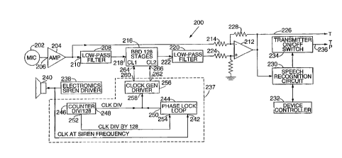
FIG. 3 schematically illustrates an analog implementation of a noise
rejection system 200 for substantially eliminating repetitive background noise
from a microphone communication system. The noise rejection system 200
comprises an information signal interface, such as a microphone 202, for
receiving an analog information or voice signal. The microphone 202 is coupled
to an analog signal amplifier 204 at an input terminal 206 An output of the
amplifier 204 is coupled to an input of a first low-~ass filter 208 at 210, and to a
negative input of a differential amplifier 212 via a resistor 214. An output of the
first low-pass filter 208 is coupled to an input of a bucket brigade audio delaydevice (BBD) 216 at 218. As shown in FIG. 3, the BBD has 128 stages, and may, for
SUBSTITUTE SHEET (RULE 26)
CA 02259641 1999-01-06
W O 98/01956 PCTrUS97/13104
example, be a charged coupled device (CCD) for transmitting the analog
information . An output of the BBD 216 is coupled to an input of a second low-
pass filter 220 at 222. An output of the second low-pass filter 220 is coupled to a
positive input terminal of the differential amplifier 212 via a resistor 224.
An output of the differential amplifier 212 is coupled to a
transmitter interface (not shown) along line 226 via a resistor 228. The output of
the differential amplifier 212 is further coupled to a speech recognition circuit 230
that is coupled to a device controller 232, and to a transmitter on/off switch 234
for activating the transmitter interface via a control line 236.
The noise rejection system further includes an input interface 237
(shown within dashed lines) or means for identif~ ing the characteristic frequency
of one or more noise sources. The input interface may be embodied by any
combination of standard components which cooperate to identify the
characteristic frequency of a noise source. An example of an input interface 237(as shown in the embodiment of FIG. 3) includes means for sensing the
characteristic frequency when the characteristic fr~quency varies with time. As
will be explained in more detail, the input interface 237 receives an analog signal
from a siren driver 238 which drives a repetitive noise generator such as a siren
or loudspeaker 240. Specifically, the input interface 237 includes a phase-locked
loop (PLL) 244 having an internal voltage-controlled oscillator (VCO) and a first
channel or referellce frequency input 242 coupled to the siren driver 238. A free
running counter~divide-by-128 circuit 246 h~s an input 248 coupled to an output
250 of the PLL 244 for receiving a voltage-controll(!d oscillator (VCO) clock signal
~enerated by the PLL 244. The counter/divide circuit 246 in turn has an output
~52 coupled to a second channel input 254 of the PLL 244 for transmitting a pulse
signal to the PLL having-a frequency 1/128 of the frequency of the VCO output ofthe PL~ 244. In other words, for every 128 pulses the counter receives from the
VCO clock output 250 of the PLL 244, the counter/divide circuit 246 sends a pulse
to the second channel input 254 of the PLL ~44. A comparator within the PLL
SlJ~;~ l l l UTE SHEET (RULE 26)
CA 022~9641 1999-01-06
W 098/01956 PCTrUS97/13104
11
compares the reference frequency of the noise signal received on the first
channel 242 to the VCO/128 signal received on the second channel 254 for
adjusting the bias of the VCO within the PLL 244 to generate a VCO clock signal
at the output 250 of the PLL having a frequency that is 128 times the frequency of
5 the noise signal.
A clock generator driver 256 has an input 258 coupled to the VCO
clock output 250 of the phase-locked loop 244. The clock generator driver 256
further includes first and second control outputs 260, 262 coupled to respectivefirst and second control inputs 264, 266 of the BBD 216.
The analog implementation of the noise reiection system 200 will
now be explained in detail. The microphone 202 receives an information signal
having an information component, such as a user's voice, and a repetitive noise
component, such as a siren signal originating from the siren driver 238 and
emanating from the loudspeaker 240. Simultaneous with the reception of the
information signal, the siren driver 238 generates a repetitive noise signal which
issues as a siren signal via the loudspeaker 240.
The noise signal having a varying characteristic frequency and
associated period is sent to the first channel or reference signal input 242 of the
PLL 244. The counter/divide circuit 246 sends a pulse to the second channel
input 254 of the PLL 244 having an instant frequency equal to that of the VCO ofthe PLL divided by 128. The reference signal and ~he VCO/128 signal are then
used by a comparator within the PLL 244 to adjust the frequency of the VCO
output signal of the PLL 244 to be 128 times the instant frequency of the siren
noise signal. The VCO clock signal is input to the clock generator driver 256
which in turn generates control signals at 260 and 262 for driving the BBD 216.
During each period of the VCO clock signal, the clock generator driver sends
control signals to the BBD at inputs 264, 266 inforlning the BBD to advance by
one stage a portion of the analog signal stoled therein. Because there are 128
stages in the BBD, and a portion of the informatio.l signal is stored in each stage
SUb~ 111 UTE SHEET (RULE 26)
CA 022~9641 1999-01-06
W O 98/01956 PCTAUS97/13104
12
1/128 of the period of the noise signal, the information signal exiting the BBD
has been delayed by a full period of the noise signal The delayed information
signal is then input to the positive input of the differential amplifier 212 to be
added with a non-delayed or current information signal received by the
5 differential amplifier 212 at its negative input. The non-delayed information
signal is in effect subtracted from the delayed information signal to generate the
processed information signal at the output of the amplifier 212. Alternatively,
the delayed information signal may be subtracted from the non-delayed
information signal in order to generate the proce~sed information signal. The
10 processed information signal may then be processed further by the device
controller 232 and the speech recognition circuit 21~0 before being sent to the
transmitter (not shown) that is activated by the transmitter on/off switch 234.
Although the delay of the information signal has been described with reference
to a full period of the noise signal, it may be desir.~ble to delay the information a
15 few full periods of the noise signal. Further, the delay may be an odd-numbered
of half periods of the noise signal. In this case, the delayed and non-delayed
information signals are added to one another in order to form the processed
information signal.
Another embodiment of the input interface or identifying means
20 may include a means for loading a predetermined clock frequency associated
with the characteristic frequency (not shown) which is supplied to the BBD 216
when the characteristic frequency is at a constant and known value. Because the
characteristic frequency is predetermined, there is no need for the PLL 244 and
the counter/divide circuit 246 to sense the characteristic frequency in order to25 generate the clock frequency for driving the B~D 216.
While the present invention has been described in preferred
embodiments, it will be understood that numerolls modifications and
substitutions can be made without departing from the spirit or scope of the
invention. Por example, the BBD of FIG. 3 may be employed to delay the
SUBSTITUTE SHEET (RULE 26)
CA 022~9641 1999-01-06
WO 98/019S6 PCT~US97/131~4
13
information signal for an odd number of half periods or a few full periods of the
noise signal in order to generate the processed information signal. The
embodiment of FIG. 3 illustrates a mainly analog implementation of the noise
rejection system, but a digital system relying primarily upon a microprocessor
5 and software or a chip, as shown in FIGS. 1 and 2, may also be employed. As was
previously mentioned, the invention also has broad application beyond
emergency vehicle communication systems. For example, the noise rejection
apparatus and method may be used in duplicated form in public address systems
at sportin~ events and in other systems where horns, whistles or other repetitive
10 noise generators, each having its own characteristic frequency or frequencies, are
functioning simultaneously. The rejection apparatus can also be used for
rejecting noise from information signals picked u~ by many other transducers in
industrial, vehicular and other environments. Accordingly, the present
invention has been described in preferred embodiments by way of illustration,
15 rather than limitation.
SUBSTITUTE SHEET (RULE 26)