Note: Descriptions are shown in the official language in which they were submitted.
CA 02260041 1999-O1-06
~;Lr-, ~'Tt~IS A'"
FHP 97-39
.~ , n y~C~!,~T",.~
DESCR=pT=ON
Radiation Detection Device and Method of Making the Same
Technical Field
The present invention relates to a radiation detection
device; and, in particular, to a radiation detection device
having a light-receiving portion with a large area, which
is used for medical X-raying and the like.
Background Art
While X-ray sensitive films have conventionally been
used for medical and industrial X-raying, radiation imaging
systems using a radiation detection device are becoming
pervasive due to their convenience and the storability of
their photographed results. Such a radiation imaging
system uses a radiation detection device having a plurality
of pixels so as to acquire, as an electric signal, two-
dimensional image data formed by a radiation, and processes
thus obtained signal with a processing unit, so as to display
it on a monitor. A typical radiation detection device is
configured such that a scintillator is disposed on one- or
two-dimensionally arranged photodetectors so as to convert
the incident radiation into light, which is then detected.
CsI, a typical scintillator material, is a hygroscopic
material which dissolves by absorbing vapor (moisture) in
the air. As a result, characteristics of the scintillator,
1
CA 02260041 1999-O1-06
FHP 97-39
such as resolution in particular, have disadvantageously
deteriorated.
Known as a radiation detection device having a
structure for protecting the scintillator against moisture
is the technique disclosed in ,Tapanese Patent Application
Laid-Open No. 5-196742. In this technique, a water-
impermeable moisture-proof barrier is formed on the upper
side of the scintillator layer, thereby protecting the
scintillator against moisture.
Disclosure of Invention
In the above-mentioned technique, however, it is hard
for the moisture-proof barrier in the outer peripheral
portion of the scintillator layer to come into close contact
with the substrate of the radiation detection device. In
particular, in a radiation detection device having a large
area used for chest X-raying or the like, due to its long
outer peripheral portion, there is a fear of peeling off
the moisture-proof barrier. Hence, the hermetic sealing of
the scintillator layer might become incomplete, moisture
penetrates into the scintillator layer; it might cause a
problem that deteriorates characteristics of the
scintillator layer.
Also, the above-mentioned technique discloses a
method of making a moisture seal layer for the moisture-proof
barrier in which a silicone potting material or the like
2
CA 02260041 1999-O1-06
FHP 97-39
is coated on the scintillator layer in a liquid state or
coated inside a window member disposed on the light-
receiving surface side of the radiation detection device
and then the window member is disposed on the scintillator
layer before the moisture seal layer is dried, thereby fixing
the moisture seal layer. In this method, it is hard to
uniformly form the moisture seal layer on a scintillator
layer having an irregular surface form, whereby adhesion
may deteriorate. This phenomenon tends to occur in
radiation detection devices having a large area, in
particular.
In view of the foregoing problems, it is an object of
the present invention to provide a radiation detection
device having a uniform protective film, which is easy to
make, for protecting the scintillator against moisture; and
a method of making the same.
In order to achieve this object, the radiation
detection device of the present invention comprises: (1)
a light-receiving device array in which a plurality of
light-receiving devices are one- or two-dimensionally
arranged on a substrate to form a light-receiving portion,
and a plurality of bonding pads electrically connected to
the light-receiving devices in respective rows or columns
of the light-receiving portion are disposed outside the
light-receiving portion; (2) a scintillator layer,
deposited on the light-receiving devices of the light-
3
CA 02260041 1999-O1-06
FHP 97-39
receiving portion, for converting a radiation into visible
light; ( 3 ) one or a plurality of resin frames made of a resin
each formed like a closed frame separating an area formed
with the scintillator layer on the light-receiving device
array and an area in which the bonding pads are arranged
from each other; and (4) a radiation-transmittable,
moisture-resistant protective film, constituted by a
multilayer film made of at least two layers including an
organic film and an inorganic film laminated thereon,
covering at least the scintillator layer and reaching above
the resin frame so as to expose at least the bonding pad
portion.
As a consequence, the incident radiation is converted
into visible light by the scintillator layer. As the
resulting visible light image is detected by the one- or
two-dimensionally arranged light-receiving devices, an
image electric signal corresponding to the incident
radiation image is obtained. The scintillator layer has a
characteristic of deteriorating by absorbing moisture. In
the present invention, however, since the scintillator
layer is covered with the moisture-resistant protective
film, which is in close contact with the light-receiving
device array with the aid of the resin frame, the
scintillator layer is completely hermetically sealed so as
to be isolated from the external atmosphere, thus being
protected against vapor in the air. Further, the bonding
4
CA 02260041 1999-O1-06
FHP 97-39
pad portion for connection with an external circuit is
exposed.
Preferably, the resin frame is formed like a rectangle
surrounding the scintillator layer or one or a plurality
of rectangles respectively surrounding their corresponding
bonding pad areas.
A coating resin for covering an edge of the
moisture-resistant protective film along the resin frame
may further be provided. In this case, the edge of the
moisture-resistant protective film is held between the
resin frame and coating resin from the upper and lower sides,
so as to be firmly bonded.
On the other hand, the method of making a radiation
detection device in accordance with the present invention
comprises: (1) a first step of forming a light-receiving
portion by one- or two-dimensionally arranging a plurality
of light-receiving devices on a substrate, and depositing
a scintillator layer for converting a radiation into visible
light on the light-receiving devices of the light-receiving
portion of a light-receiving device array in which a
plurality of bonding pads electrically connected to the
light-receiving devices in respective rows or columns of
the light-receiving portion are disposed outside the
light-receiving portion; ( 2 ) a second step of forming with
a resin, on the light-receiving device array, one or a
plurality of resin frames each formed like a closed frame
5
CA 02260041 1999-O1-06
FHP 97-39
separating the scintillator layer and a bonding pad portion
from each other; (3) a third step of forming a
radiation-transmittable first organic film enveloping the
light-receiving device array as a whole; ( 4 ) a fourth step
of laminating at least one layer of film including an
inorganic film on the first organic film so as to form a
radiation-transmittable, moisture-resistant protective
film constituted by a multilayer film made of at least two
layers; and (5) a fifth step of cutting the moisture-
resistant protective film along a longitudinal direction
of the resin frame and removing the moisture-resistant
protective film on the bonding pad portion so as to expose
the bonding pad portion.
As the f first organic film is formed such as to envelope
the light-receiving device array as a whole, the adhesion
between the scintillator layer and the organic film improves,
thereby forming a uniform film. As the moisture-resistant
protective film is removed from the bonding pad portion after
being formed, the bonding pad portion is securely exposed.
The resin frame formed under the protective film adds a
margin to the cut-in depth of a cutter when cutting the
protective film. Further, the resin frame brings edges of
the protective film into close contact with the substrate,
thereby assuring the sealing.
A sixth step of covering and bonding an edge of the
moisture-resistant protective film along the resin frame
6
CA 02260041 2001-O1-17
27986-13
with a resin may further be provided after the fifth step. In
this case, the edge of the moisture-resistant protective film
is held between the resin frame and this resin so as to be
firmly bonded.
In accordance with the present invention, there is
provided a radiation detection device comprising: a light-
receiving device array in which a plurality of light-receiving
devices are one- or two-dimensionally arranged on a substrate
to form a light-receiving portion, and a plurality of bonding
pads electrically connected to said light-receiving devices in
respective rows or columns of said light-receiving portion are
disposed outside said light-receiving portion; a scintillator
layer, deposited on said light-receiving devices of said light-
receiving portion and provided with columnar crystals, for
converting a radiation into visible light; one or a plurality
of resin frames made of a resin each formed like a closed frame
separating an area formed with said scintillator layer on said
light-receiving device array and an area in which said bonding
pads are arranged from each other; and a radiation-
transmittable, moisture-resistant protective film covering at
least the top and side portions of said scintillator layer and
the surface of said light-receiving array around said
scintillator layer and reaching above said resin frame so as to
expose at least said bonding pad portion, said protective film
intrudes into gaps among the top part of said columnar
crystals.
In accordance with the present invention, there is
also provided a method of making a radiation detection device
comprising steps of: (a) forming a light-receiving portion by
one- or two-dimensionally arranging a plurality of light-
receiving devices and a plurality of bonding pads disposed
outside said light-receiving portion and electrically connected
7
CA 02260041 2001-O1-17
27986-13
to said light-receiving devices in respective rows or columns
of said light-receiving portion on a substrate; (b) depositing
a scintillator layer provided with columnar crystals for
converting a radiation into visible light on said light-
s receiving devices of said light-receiving portion of a light-
receiving device array; (c) forming with a resin, on said
light-receiving device array, one or a plurality of resin
frames each formed like a closed frame separating said
scintillator layer and a bonding pad portion from each other;
(d) forming a radiation-transmittable, moisture resistant
protective film enveloping said light-receiving device array as
a whole so as to cover the top and side portions of said
scintillator, the surface of said light-receiving device array
around said scintillator, and the top and side part to said
resin frames and intrude into gaps among the top part of said
columnar crystals; (e) cutting said moisture-resistant
protective film at the top portions of said resin frame along a
longitudinal direction of said resin frame; and (f) removing
said moisture-resistant protective film on said bonding pad
portion so as to expose said bonding pad portion.
Brief Description of Drawings
Fig. 1 is a top plan view showing an embodiment of
the present invention, whereas Fig. 2 is an enlarged sectional
view thereof taken along the line A-A;
Figs. 3 to 11 are views showing manufacturing steps
of the embodiment in accordance with Figs 1 and 2; and
Fig. 12 is a top plan view showing another embodiment
of the present invention, whereas Fig. 13 is an enlarged
sectional view thereof taken along the line B-B.
7a
CA 02260041 2001-O1-17
X7986-13
Best Mode for Carrying Out the Invention
In the following, preferred embodiments of the
present invention will be explained with reference to the
drawings. To facilitate the comprehension of the exp7_anation,
the same reference numerals denote the same parts, where
possible, throughout the drawings, and a repeated explanation
will be omitted. Also, the dimensions and forms in each
drawing are not always identical to those in practice but
include parts exaggerated to facilitate. understanding.
Fig. 1 is a top plan view showing an embodiment of
the present invention, whereas Fig. 2 is an enlarged sectional
7b
CA 02260041 1999-O1-06
FHP 97-39
view of its outer peripheral portion taken along the line
A-A.
First, the configuration of this embodiment will be
explained with reference to Figs . 1 and 2 . On an insulating
substrate 1, such as that made of glass, for example,
light-receiving devices 2 for effecting photoelectric
conversion are arranged two-dimensionally, so as to form
a light-receiving portion. Each light-receiving device 2
is constituted by a photodiode (PD) made of amorphous silicon
or a thin-film transistor (TFT). The light-receiving
devices 2 in the respective rows or columns are electrically
connected to each other via signal lines 3 for reading out
signals. A plurality of bonding pads 4 for taking out
signals to an external circuit (not shown) are disposed along
outer peripheral sides, e.g., two adjacent sides, of the
substrate 1 and are electrically connected to their
corresponding plurality of light-receiving devices 2 via
the signal lines 3. An insulating passivation film 5 is
formed on the light-receiving devices 2 and signal lines
3. For the passivation film 5, silicon nitride or silicon
oxide is preferably used. On the other hand, the bonding
pads 4 are exposed for connection with the external circuit.
In the following, this substrate and the circuit portion
on the substrate are referred to as a light-receiving device
array 6.
Formed on the light-receiving portion of the
8
CA 02260041 1999-O1-06
FHP 97-39
light-receiving device array 6 is a scintillator 7, having
a columnar structure, for converting an incident radiation
into visible light. Though various materials can be used
for the scintillator 7, T1-doped CsI or the like, which has
a favorable emission efficiency, is preferable. A resin
frame 8 formed like an elongated frame from a resin is
disposed at a position inside the bonding pads, so as to
surround the outer periphery of the light-receiving device
array 6. As this resin frame 8, KJR651 or KE4897
manufactured by Shin-Etsu Chemical Co., Ltd., TSE397
manufactured by Toshiba Silicone Co., Ltd., and DYMAX625T
manufactured by Sumitomo 3M Ltd. , which are silicone resins,
and the like are preferably used. This is because they are
widely used for surface processing for mechanically and
electrically protecting semiconductor devices and exhibit
high adhesion to a protective film 12 formed on the upper
side which will be explained later.
Laminated on the scintillator 7 inside the frame of
the resin frame 8 are a first organic film 9, an inorganic
film 10, and a second organic film 11, each transmitting
X-rays therethrough but blocking vapor, thereby forming a
protective film 12.
As the first organic film 9 and the second organic film
11, a poly-para-xylylene resin (manufactured by Three Bond
Co., Ltd.; trade name: Parylene), such as poly-para-
chloroxylylene (manufactured by the same company; trade
9
CA 02260041 1999-O1-06
FHP 97-39
name: Parylene C) in particular, is preferably used. The
coating film made of Parylene has excellent characteristics
suitable for the organic films 9, 11 in that, for example,
it transmits therethrough only a very small amount of vapor
and gasses, has high water repellency and chemical
resistance, exhibits excellent electrical insulation even
in a thin film, and is transparent to radiation and visible
light. The details of the coating with Parylene are
described in Three Bond Technical News (issued September
23, 1992), and their characteristics will be noted here.
Parylene can be coated by chemical vapor deposition
(CVD) method in which it is vapor-deposited on a support
in vacuum as with the vacuum vapor deposition of metals.
This method comprises a step of thermally decomposing
p-xylene, which is a raw material, and rapidly cooling the
resulting product in an organic solvent such as toluene or
benzene, so as to yield di-para-xylylene which is known as
dimer; a step of thermally decomposing this dimer so as to
generate a stable radical para-xylylene gas; and a step of
causing thus generated gas to be absorbed and polymerized
on a material so as to form a poly-para-xylylene film having
a molecular weight of about 500,000 by polymerization.
The pressure at the time of Parylene vapor deposition
is 0.1 to 0.2 torr, which is higher than the pressure in
the case of metal vacuum vapor deposition, 0.001 torr. Upon
vapor deposition, a monomolecular film covers the whole
CA 02260041 1999-O1-06
FHP 97-39
material to be coated, and then Parylene is vapor-deposited
thereon. Consequently, a thin film having a thickness as
small as 0.2 ~,m can be formed with a uniform thickness in
the state free of pinholes . Therefore, the coating on acute
angle portions, edge portions, and narrow gaps of the order
of microns, which has been impossible in the liquid form,
can be effected. Also, the coating can be effected at a
temperature close to room temperature, without needing heat
treatment and the like at the time of coating. As a
consequence, mechanical stress or thermal distortion
accompanying hardening would not occur, and the coating is
excellent in stability as well. Further, coating is
possible with respect to almost any solid material.
For the inorganic film 10, various materials such as
those transparent, opaque, or reflective to visible light
can be used as long as they can transmit X-rays therethrough.
Oxidized films of Si, Ti, and Cr, and metal thin films of
gold, silver, aluminum, and the like can be used. In
particular, a film reflective to visible light is preferably
used, since it is effective in preventing fluorescence
generated in the scintillator 7 from leaking out, thereby
enhancing sensitivity. Here, an example using A1 which is
easy to shape will be explained. Though A1 itself is likely
to corrode in the air, the inorganic film 10 is protected
against corrosion since it is held between the first organic
film 9 and the second organic film 11.
11
CA 02260041 1999-O1-06
FHP 97-39
While this protective film 12 is formed by the
above-mentioned Parylene coating, since it is formed by CVD
method, it is formed such as to cover the whole surface of
the light-receiving device array 6. Therefore, in order to
expose the bonding pads 4, it is necessary that the
protective film 12 formed by the Parylene coating be cut
inside the bonding pads 4, and the outer part of the
protective film 12 be removed. As will be mentioned later,
when the protective film 12 is cut near substantially the
center of the frame portion of the resin frame 8, the outer
peripheral portion of the protective film 12 would be fixed
by the resin frame 8, whereby the protective film 12 can
be prevented from peeling off from the outer peripheral
portion. Further, the outer peripheral portion of the
protective film 12, together with the resin frame 8
thereunder, is coated with a coating resin 13. For the
coating resin 13, a resin which favorably adheres to the
protective film 12 and resin frame 8, such as WORLD ROCK
No. 801-SET2 (70,000 cP type) manufactured by Kyoritsu
Chemical Industries Co. , Ltd. , which is an acrylic adhesive,
for example, is preferably used. This resin adhesive is
hardened in about 20 seconds upon UV irradiation at 100 mW/cmz.
Thus hardened coating film is soft but has a sufficient
strength, is excellent in resistances to moisture, water,
galvanic corrosion, and migration, favorably adheres to
various materials such as glass, plastics, and the like in
12
CA 02260041 1999-O1-06
FHP 97-39
particular, and thus has favorable characteristics as the
coating resin 13. Alternatively, the same silicone resin
as the resin frame 8 may be used. Also, the same acrylic
adhesive as the coating resin 13 may be used for the resin
frame 8.
The manufacturing process of this embodiment will now
be explained with reference to Figs . 3 to 11 . As shown in
Fig. 4, columnar crystals of T1-doped CsI are grown according
to vapor deposition method by a thickness of 600 ~,m on the
light-receiving surface of thelight-receiving device array
6 shown in Fig. 3, so as to form a layer of the scintillator
7.
On the other hand, as shown in Fig. 5, between the
respective outer peripheries of the light-receiving portion
and light-receiving device array, the resin frame 8 is formed
like an elongated frame having a width of 1 mm and a height
of 0.6 mm on the passivation film 5 inside the bonding pads
4 along the outer perimeter of the light-receiving portion.
For forming this frame, for example, an automatic x-Y coating
apparatus such as AutoShooter-3 manufactured by Iwashita
Engineering Ltd. is preferably used. At this time, for
further improving the adhesion to the first organic film
9 formed on the upper side, it will be more preferable if
the surface of the resin frame 8 is subjected to a
rough-surface treatment. Examples of the rough-surface
treatment include scoring and forming a number of small
13
CA 02260041 1999-O1-06
FHP 97-39
depressions on the surface.
CsI, which forms the layer of scintillator 7 is highly
hygroscopic, so that it dissolves by absorbing vapor in the
air when left exposed. In order to prevent this phenomenon
from occurring, as shown in Fig. 6, CVD method is used for
enveloping the whole substrate with Parylene at a thickness
of 10 Vim, thereby forming the first organic film 9. Though
there are gaps among the columnar crystals of CsI, Parylene
intrudes into these narrow gaps to some extent, whereby the
first organic film 9 comes into close contact with the
scintillator layer 7. Further, the Parylene coating yields
a precision thin film coating with a uniform thickness on
the layer of scintillator 7 having irregularities. Since
Parylene can be formed by CVD at a lower vacuum than in the
case with the metal vapor deposition and at normal
temperature as mentioned above, it can be processed easily.
Further, as shown in Fig. 7, an A1 film having a
thickness of 0.2 ~m is laminated on the surface of the first
organic film 9 on the entrance side by vapor deposition
method, thus forming the inorganic film 10. Then, by using
CVD method again, the surface of the whole substrate is
coated with Parylene at a thickness of 10 ~,m, thereby forming
the second organic film 11 ( see Fig. 8 ) . This second organic
film 11 prevents the inorganic film 10 from deteriorating
due to corrosion.
Thus formed protective film 12 is cut with a cutter
14
CA 02260041 2000-OS-08
27986-13
14 along the longitudinal direction of the resin frame 8 (see
Fig. 9). Since the resin frame 8 forms a protrusion, the cut
portion is easily confirmed. Also, since the thickness of the
resin frame 8 forms a margin for inserting the cutter 14, there
is no fear of the signal lines 3 under the resin frame 8 being
damaged. Hence, the processing becomes easier, thereby
improving the yield of the product. Thereafter, from thus cut
portion, the parts of the protective film 12 on the outer side
thereof and the rear side of the entrance surface are removed,
so as to expose the bonding pads 4 for connection with the
external circuit (see Fig. 10). Thereafter, the outer
peripheral portion of the protective film 12 and the exposed
resin frame 8 are coated and covered with a coating resin 13,
which is then hardened upon UV irradiation (see Fig. 11).
In general, the passivation film 5 and the first
organic film 9 do not adhere to each other well. In accordance
with the configuration of this embodiment, however, since the
resin frame 8 adapted to closely adhere to both of the first
organic film 9 and the passivation of film 5 is disposed
therebetween, the first organic film 9 comes into close contact
with the passivation film 5 with the aid of the resin frame 8.
Through the protective film 12 will closely adhere to the
light-receiving device array 6 with the aid of the resin frame
8 even if the coating resin 13 is not provided, the coating
resin 13 is preferably formed since the protective film 12
including the first organic film 9 would be fixed thereby as
being held between the resin frame 8 and the coating resin 13,
thus further improving the adhesion of the protective film 12
onto the light-receiving device array 6. As a consequence, the
scintillator 7 is hermetically sealed with the protective film
12, whereby moisture can securely be prevented from intruding
into the scintillator 7, thus making it possible to keep the
CA 02260041 2000-OS-08
27986-13
resolution of device from decreasing due to the deterioration
of the scintillator 7 caused by moisture absorption.
The operation of this embodiment will now be
explained with reference to Figs. 1 and 2. An incident X-ray
(radiation) from the entrance surface side is transmitted
though all of the first organic film 9, inorganic film 10, and
second organic film 11, so as to reach the scintillator 7.
This X-ray absorbed by the scintillator 7, which radiates
visible light in proportion to the dose of the X-ray. Of thus
radiated visible light, the part directed opposite to the
incident direction of the X-ray is transmitted through the
first organic film 9 so as to be reflected by the inorganic
film 10. As a consequence, substantially all the visible light
generated by the scintillator 7 is made incident on the light-
receiving device 2 by way of the passivation film 5. Hence,
efficient detection can be effected.
16
CA 02260041 1999-O1-06
FHP 97-39
In each light-receiving device 2, an electric signal
corresponding to the light quantity of the visible light
is generated by photoelectric conversion and is stored for
a predetermined period of time. Since the light quantity
of the visible light corresponds to the dose of the incident
X-ray, the electric signal stored in each light-receiving
device 2 corresponds to the dose of the incident X-ray,
whereby an image signal corresponding to an X-ray image is
obtained. The image signals stored in the light-receiving
devices 2 are sequentially read out from the bonding pads
4 via the signal lines 3, transferred to the outside, and
processed in a predetermined processing circuit, whereby
the X-ray image can be displayed.
Though the foregoing explanation relates to the
protective film 12 having a configuration in which the
inorganic film 10 is held between the first and second
organic films 9, 11 made of Parylene, the first organic film
9 and the second organic film 11 may be made of materials
different from each other. Also, when a material highly
resistant to corrosion is used for the inorganic film 10,
the second organic film 11 per se may be omitted.
Though an example in which the resin frame 8 and the
coating resin 13 are formed on the passivation film 5 outside
the part formed with the light-receiving devices 2 is
explained here, it will be difficult to form the resin frame
8 at a boundary portion between the light-receiving device
17
CA 02260041 1999-O1-06
FHP 97-39
2 and the bonding pad 4 if they are located close to each
other. For securely exposing the bonding pad 4 and securely
coating the periphery of the protective film 12 with the
coating resin 13, it is preferred that the positions of the
resin frame 8 and coating resin 13 be shifted toward the
light-receiving device 2. To this end, the scintillator 7
is not formed on the whole surface on the light-receiving
devices 2 but on the light-receiving devices 2 in the
effective screen area excluding the pixels near the bonding
pads 4. Then, after the resin frame 8 is formed outside the
effective screen area, i.e., on the ineffective pixels, the
protective film 12 is formed so as to cover the formed layer
of scintillator 7 as a whole and reach the resin frame 8.
Thereafter, the protective film 12 is cut along the
longitudinal direction of the resin frame 8, the part of
the protective film 12 outside the effective screen area
is removed, and then the edges of the protective film 12
are coated with the coating resin 13 along the resin frame
8. In this case, since the pixels near the bonding pads 4
are covered with the resin frame 8 and the coating resin
13 or are free of the scintillator 7 on the front side, their
sensitivity to the radiation decreases. As a result, these
pixels are unusable, thus reducing the number of effective
pixels and effective screen area in the light-receiving
devices 2. When the light-receiving devices 2 constitute
a large screen and have a large number of pixels in total,
18
CA 02260041 1999-O1-06
FHP 97-39
however, the ratio of the ineffective pixels is small and,
depending on the configuration of devices, they may yield
a merit that manufacturing becomes easier.
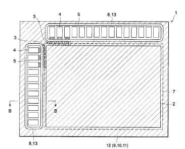
With reference to Figs. 12 and 13, another embodiment
of the present invention will now be explained. Fig. 12 is
a top plan view of the radiation detection device in
accordance with this embodiment, whereas Fig. 13 is an
enlarged sectional view thereof taken along the line B-
B. Since the basic configuration of this device is
basically the same as that of the embodiment shown in Figs.
1 and 2, only their differences will be explained in the
following.
In the embodiment shown in Figs. 12 and 13, the
protective film 12 is formed on the whole surface of the
light-receiving device array 6 on the light-receiving
surface side and the rear side, exposing only the bonding
pad array 4 portion. The resin frame 8 is formed such as
to surround the exposed bonding pad array 4 portion, and
the coating resin 13 is coated on the resin frame 8 along
the boundaries ( edges ) of the protective film 12 . Since the
bonding pad 4 portion is securely exposed, and the protective
film 12 securely adheres to the light-receiving device array
6 with the aid of the resin frame 8 and coating resin 13,
the layer of scintillator 7 is hermetically sealed, whereby
it can be prevented from deteriorating due to moisture
absorption in this embodiment as well.
19
CA 02260041 1999-O1-06
FHP 97-39
This embodiment is effective in that it can reduce the
length of the edge portion acting as a boundary portion which
may cause the protective film to peel off, in particular,
in the case of CCD or MOS type imaging devices in which the
bonding pad portion 4 is small.
Further, though the foregoing explanation relates to
so-called surface entrance type radiation detection devices
in which radiation is incident thereon from the scintillator
side on light-receiving devices, the present invention is
also applicable to so-called rear face entrance type
radiation detection devices . Such a rear face entrance type
radiation detection device can be used as a high-energy
radiation detection device.
As explained in the foregoing, for protecting a highly
hygroscopic scintillator, a protective film made of
Parylene or the like is formed on the scintillator, and the
outer periphery of the protective film is bonded to the
light-receiving device array with a resin layer, whereby
the scintillator layer is hermetically sealed in accordance
with the present invention. In particular, since the
peeling from the edges of the protective film is prevented
from occurring, resistance to moisture would be improved.
Further, if these edges are covered with a coating
resin, the hermetic sealing will further be improved, thus
enhancing the resistance to moisture.
In the manufacturing method of the present invention,
CA 02260041 1999-O1-06
FHP 97-39
the protective film is formed and then unnecessary parts
thereof are removed, whereby the protective film in a uniform
state is formed more easily as compared with the case where
the protective film is formed on only necessary parts, while
securely exposing the bonding pads. Also, since the
protective film penetrates through the gaps among the
columnar crystals in the scintillator layer, the adhesion
between the protective film and scintillator layer
increases. Further, since the thickness of the resin layer
provides a cut-in margin for the cutter when cutting, the
signal lines for reading out detected signals would not be
damaged even when the accuracy of the cutting tool is not
enhanced, thereby improving the yield of the product.
From the invention thus described, it will be obvious
that the invention may be varied in many ways. Such
variations are not to be regarded as a departure from the
spirit and scope of the invention, and all such
modifications as would be obvious to one skilled in the art
are intended for inclusion within the scope of the following
claims.
Industrial Applicability
The radiation detection device in accordance with the
present invention is applicable to a large-area radiation
imaging system used for medical and industrial X-raying in
particular. It can be used for chest X-raying or the like
21
CA 02260041 1999-O1-06
FHP 97-39
in place of X-ray films which are currently in wide use in
particular.
22