Note: Descriptions are shown in the official language in which they were submitted.
CA 02260103 1999-01-08
WO98/03011 PCT~P97/03513
~MAG~G APPARATUSHAV'~G ALARGESENS'~G AR'~A
The invention relates to im:~ging apparatus. The invention finds particular
application to large area imaging.
S Trn~gin~J systems are used in a wide range of applications, particularly for
imaging for medical diagnosis, in biotechnology and in industrial applications for non-
destructive testing and on-line product quality control.
For all of these fields of application, prevailing means of performing im~ging
is with the use of radiation, usually X-rays, gamma-rays and beta-rays. Radiation is
detected by some sort of imaging plane, which need not be planar. Accordingly, the
term im~ging surface will be used hereinafter. Images are formed either directly on
the in~?ging surfaces (e.g. projection im~ging) or data are processed and images are
reconstructed in a computer (e.g. computerized tomography or coded aperture
im~ging in nuclear medicine).
The traditional im~ging surface was formed by a film in a cassette. Other
im~ging surface solutions have been developed over the past 40 years offering digital
im~ging Such examples are NaI scintill~ting screens, NaI scintill~ting crystals, BGO
crystals, wire gas chambers, digital im~ging plates etc. More recently, semiconductor
im:~ging solutions such as Charged Coupled Devices, Si microstrip detectors and
semiconductor pixel detectors have been developed.
Typically, in all of the above cases, when a large im~ing area is needed it is
made either as a monolithic structure (e.g. films, digital im~ging plates, NaI screens
etc.) or as a mosaic of smaller pieces (tiles) put together and fixed on a support
surface (e.g. gamma cameras with NaI crystals).
When a monolithic large im~ginlJ surface is employed, if a part of the surface
is defective then the whole surface needs to be changed. Unfortunately, the most~ precise digital on-line im~ging devices proposed so far involve pixel-based
semiconductors which cannot be manufactured in large areas (larger than a few square
cm at most). Moreover, it would not be desirable to manufacture, for example, a
monolithic 30cm by 30cm digital imaging semiconductor surface because the yield
would be low. If a portion of the expensive imaging area became defective, then the
..... . . ..
CA 02260103 1999-01-08
WO 98/03011 PCT/EP97/03513
whole surface would have to be replaced.
It has been proposed to provide a large area imaging surface (larger than a few
square mm) using a tiling approach. In the applicant's patent application WO
95/33332, it has been proposed to employ a tiling approach. Using such an
approach, individual im~ging devices are arranged in an array, or mosaic on an
im~ging support to form a large area im~gin~ mosaic Outputs from the individual
im~ging devices can be processed to provide a single output image corresponding
substantially to the whole area covered by the imaging surface. However, when the
imaging devices are tiled to form such a mosaic, dead spaces are left around the10 active im~ging areas of the im~ging devices. In order to deal with this problem it is
proposed to stagger adjacent rows of im:~ging devices in the array and to provide for
relative movement between an object to be imaged and the im~ing array. Although
such an approach does give good results and means that the effect of the dead spaces
can be at least substantially elimin~t~.~l, this does require the provision of the
15 mechanism for the relative movement and appropriate software for processing the
resultant multi-exposure image.
An object of the invention is to provide an im~ging system and method which,
while providing the advantages of the tiling approach, remove or at least mitigate the
problems of the prior art.
In accordance with a first aspect of the invention, there is provided im~ginP
apparatus comprising an im~ging support and a plurality of im~ging device tiles,wherein each tile comprises an im~ging device having an im~ging surface and has a
non-active region at or adjacent an edge of the tile, the im~ging device on the tile
mounted on the support being tilted, or angled, such that part of the imaging surface
25 of one tile at least partially overlies the non-active region of another tile, thereby
provided subst~nti~lly continuous im~ging in a first direction.
Embodiments of the invention provide a new im~ging mosaic system for
producing imaging mosaics using a plurality of imaging devices tiles and an imaging
support in a manner which reduces or substantially elimin~tes the dead spaces
30 between tiles.
In a preferred embodiment, which enables the use of a planar support, each
CA 02260103 1999-01-08
WO 98/03011 PCT/EP97/03513
tile comprises a mount having a mounting surface for mounting the tile on the support
and a structure for carrying the imaging device on the mount such that the imaging
surface is tilted with respect to the mounting surface. In the preferred embodiment
of the structure comprises an intermediate member between the imaging device andS the mount, the intermediate member being wedge-shaped to fully support the im~ging
device. However, alternatives are possible, for example spacers at one end of the
tile.
In an alternative embodiment which enables the use of planar tiles, each tile
comprises a mount having a mounting surface for mounting the tile on the support,
the support provides a plurality of respective tile mounting locations on a support
surface, the mounting locations being tilted to provide sawtooth deviations from the
support surface, whereby the im~ging surface of each im~ging device is tilted with
respect to the support surface.
Preferably the mount is planar and more preferably a printed circuit board.
Preferably also, the im~ging device is planar, for example comprising a planar
detector layer overlying a planar image readout layer, a surface of the detector layer
forming the im~ging surface. The detector layer can provide a plurality of detector
cells and the readout layer can provide a plurality of corresponding readout circuits,
each readout circuit being coupled to a respective detector cell.
In a preferred embodiment the detector layer is subst~nti~lly rectangular, the
readout layer is substantially rectangular and has a connection region which extends
beyond the detector layer at one end thereof, the mount is substantially rectangular
and has a connection region which extends beyond the readout layer at the one end,
wired connections are provided between the connection regions of the readout layer
and the mount, and the non-active region of the tile comprises the connection regions
of the readout layer and the mount. The tile is preferably elongated in the first
direction to minimi.~e the angle of tilt and the effects of parallax.
Preferably, the tiles are mounted on the support such that the detector layers
- of adjacent tiles extend in a second direction perpendicular to the first direction so as
almost or aclually to touch each other.
Preferably, the imaging devices are positioned and held on the support in a
CA 02260103 1999-01-08
WO 98/03011 PCT/EP97/03513
reversible and non-destructive way. The removable positioning/fixing means allowindividual im~ging devices to be removed multiple times so that the same imagingdevice can be used in a different imaging support or it can be replaced if found to be
defective without (l~m~gin~ the im~ging support and without affecting the operation
5 of any other im~ginP device on the imaging support.
Preferably, the support provides a plurality of tile mounting locations, the
removable mounting means removably mounting a respective tile at each location.
In preferred embodiments, each tile mounting location comprises a plurality
of support contacts, each for co-operating with a respective tile contact for a transfer
10 of signals between the support and the tile.
The support contacts can comprise recesses for receiving correspondingly
shaped bumps on a tile or bumps for receiving correspondingly shaped recesses ona tile. More preferably, the support contacts comprise resilient conductive members
overlying contact pads.
In a preferred embodiment, the im:~ging apparatus comprises a separate
in~ ting substrate, which is located between the im~ging device tile(s) and the
im~3ging support and is aligned to enable electrical contact between each support
contact and a corresponding tile contact via a respective resilient contact member.
In this embodiment, each resilient conductive member is a ring having a hole for20 aligning bumps of the tile contacts or of the support contacts with corresponding
contacts of the support, or corresponding contacts of the tile, respectively. The
resilient conductive members can comprise conductive rubber, conductive polymersor metal springs.
Preferably, the mounting arrangement is adapted to apply an adjustable
25 mounting force for removable mounting a tile at a tile mounting location. Themounting arrangement can comprise a hole for each tile mounting location, the hole
being of appropriate diameter to accommodate securing means protruding from the
tile. Fastening means for en~ging with the securing means can be provided for each
hole on the support at each tile mounting location. In a preferred embodiment, the
30 fastening means is a nut and the securing means is a screw, the nut being adapted to
be tightened on the screw after the im~ging device tile has been positioned on the tile
CA 02260l03 l999-0l-08
WO 98/03011 PCT/EP97/03513
s
mounting location with the screw extending through the hole, whereby the nut is used
to secure the tile at the tile mounting location with an adjustable mounting force. The
mounting arrangement can comprise a screw located or locatable at each imaging
device tile location, for eng~ginP with a threaded hole in a mount of an imagingS device tile.
The im~ging apparatus can comprise a plurality of different im~ginn supports
and a common set of im~ing device tiles which are mountable on a selected imaging
support at any one time, but are removable, whereby they may be mounted on
another one of the im~ginsJ supports.
In accordance with another aspect of the invention, there is provided an
im~gin~ support for apparatus as described, above, the im~ging support providing a
plurality of respective tile mounting locations on a support surface, the mounting
locations being tilted to provide sawtooth deviations from the support surface. The
support preferably comprises an arrangement for removable mounting an im~ging
15 device tile at each mounting location in a non-destructive, removable manner. The
support enables the use of a planar im~ging device tile.
In accordance with a further aspect of the invention, there is provided an
im~ging device tile for im~ging apparatus as described above, wherein the tile
comprises an im~gin~ device having an im~ging surface, a non-active region at or20 adjacent an edge of the tile, a mount having a mounting surface for mounting the tile
on an im:lging support and a structure for supporting the im:lging device on the mount
such that the im~ging surface is at an angle to the mounting surface. This form of
im~ging device tile enables the use of a support which does not have sawtooth
deviations for the tile mounting locations.
Embodiments of the invention are described hereinafter, by way of example
only, with reference to the accompanying drawings in which:
Figure lA is a schematic cross-sectional view of part of an imaging support;
Figure lB is a schematic cross-sectional view of the part of the im~ging
support of Figure lA with one example of an im:~ging device having a mount;
Figure lC are a schematic view of the underside and apart cross-sectional
view of the side of the im~sging device mount for the im~in~ device of Figure B;
... , .. , . . . . ~ . . . ... ..
CA 02260l03 l999-0l-08
WO 98/03011 PCT/EP97/03513
Figure lD is a schematic cross-section view of apart of the im~in~J support
of Figure lB with the imaging device of Figure lB mounted thereon;
Figures 2A - 2D are views corresponding to those of Figure 1 for a second
example of an im~ging device mount; and
Figure 3A is a schematic plan view of an arrangement of four im~ging devices
mounted on an im~ging support in according with one example of the invention;
Figure 3B is a cross-sectional view of the arrangement of Figure 3A along line
B-B; and
Figure 3C is an end view of the arrangement in figure 3A in the direction of
10 arrow C in Figure 3A.
Before describing a particular embodiment of the invention, examples of
possible approaches to removable mounting of imaging devices will be described.
The removable mounting of im~ging devices forms the subject-matter of the
applicant's UK patent applications GB 9605978.7 and GB 9517608.7.
In a preferred embodiment of the present invention, by way of example only,
the im~ging devices comprise Active Semiconductor ~m~ging Devices (ASIDs) as
described in the applicant's patent application WO 95/33332. An ASID is an active,
dynamic semiconductor pixel im~ging device with dimensions from, possibly, a fewsquare mm to several square cm.
A cross-section of one such imaging device tile 24 is shown schem~tir~lly in
Figure lB over a tile mounting location on a circuit board 9 of an imaging support.
Figure lA is a schematic cross-section illustrating the application of an in.~ul~ting
layer 29 and conductive rubber rings 16 over the circuit board 9. Figure lC provides
a view of the underside and a cross-section view of an im~ging device mount (e.g.
25 a PCB) 5. Figure lD is a cross-sectional view of an im~ginsg deice tile 24 secured
a~ a tile mounting location by engagement of a nut 33 over a screw 31 of the imaging
device tile 24.
The surface area of the im~ging device 20 can vary depending on the
application and the semiconductor materials chosen. Typical sizes are of the order
30 of one square millimetre to several square centimetres, although the invention is not
limited to irnaging devices of these sizes. Radiation enters a semiconductor detector
CA 02260l03 l999-0l-08
WO 98/03011 PCT/EP97/03513
1 from an im~ging surface (the top face in Figure lB) and upon absorption creates
an electric charge. On the exit face of the detector layer 1, electrode pads (not
shown) define the detector cells or pixels. Charge created from successive radiation
hits is accumulated on the corresponding pixel circuits in a readout layer 3 which are
coMected to the detector pixels via conductive microbumps 2 (e.g. indium bumps -not shown). The pixel circuits are formed on a semiconductor readout chip which
forrns the readout layer 3. The im~ging device 20, formed by the detector layer 1
and the readout layer 3, is mounted on a mount 4, for example a printed circuit board
(PCB). The imAging device tile 24 is forrned by the combination of the imAging
10 device 20 and the mount 4.
Each im~ging device 20 has tens of thousands of pixels but only needs around
5-15 external lines that will provide control signals, supply voltage and will readout
the signal. These lines are provided on the PCB 4 and also on a circuit board 9 of
an imAging support on which the imA~in~ device tile 24 is mounted. The imaging
15 device 24 itself carries a number of contacts 5 in the form of, for example, small
metal spheres or bumps. The number of contacts typically corresponds to the number
of external lines. The metal bumps 5 match an equal number of small appropriately
sized contacts 7 on the circuit board 9 of the imAging support. The contacts on the
circuit board 9 of the im~ging support are connected to the aforementioned control,
20 supply and signal lines (not shown). In the present example, an intermediate
in.c-llAtin~ layer 29 is provided between the im~ging device mount 4 and the circuit
board 9 of the imA~ing support. Holes 30 are provided in the in.snlAting layer at
positions corresponding to the metal bumps 5 and the contacts 7. Conductive rubber
rings 16 are located in the holes 30 in the insulating layer 29.
Good electrical connection between each contact bump on the im~ging device
mount 4 and the corresponding contact 7 on the circuit board 9 is ensured by a
separate conductive rubber ring 16. These are placed in appropriate holes of theelectrically inclllAting layer 29, which is aligned and glued on top of the circuit board
9. The use of conductive rubber rings (i.e. with holes) is not essential, and
30 conductive flexible pads could be used instead. However, the use of a ring structure
with a central hole is advantageous for aiding alignment of the imaging device.
.. , .... . ~
CA 02260103 1999-01-08
WO 98/03011 PCT/EP97/03513
Alternatives to the conductive rubber rings 16, such as conductive polymers or metal
springs, may be used. A screw 31 is glued into a hole 34 in the im~gino device
mount 4. This screw is pushed through the hole 32 in the circuit board 9 of the
imaging support and is secured by the nut 33. The nut is tightened to press the metal
5 balls 5 of the im~ging device mount 4 against the rubber rings 16 which in turn are
pressed against the metal pads 7 of the im~ging support circuit board 9 ensuring good
electrical contact.
This embodiment is particularly suitable for providing an imaging area
comprising a plurality of easily removable semiconductor pixel im~ging devices as
described in WO 95/33332, or other types of pixel semiconductor im~ging devices.As individual im~ging devices can be removed and re-positioned any number
of times, the same im~ging devices can be used in a number of applications. For
example imaging devices used for mammography can be quickly transferred on a
different im~ging support for chest X-rays. A variety of im~ging supports can have
15 different sizes and shapes but only one set of im~ging devices is needed. Additionally
replacing an im~ging device can be done by a non-expert and m~int~n~n~e costs are
minimi7P~. Accordingly, contrary to the prior art where large im~ging areas havemonolithic im~,,ing means or a fixed tiled im~ging plane, the invention introduces a
new large area im~ging system where the im~ginsJ mosaic is made of removable
20 im~ging devices allowing for multi-purpose use and re-use of the individual im~gino
devices, while also allowing cost effective maintenance of the im~ging areas.
If a particular example, e.g. mammography, is considered, an im~ging surface
of 30cm by 30cm (about 600 im:~ging devices of the type described in patent
application W095/33332) will be needed. The 600 im~ging devices will be mounted
25 on a printed circuit board 9 of the im~gino support.
By means of the screws and nuts it is also possible individually IO adjust the
mounting force for each imaging device to ensure good alignment and good electrical
contact using flexible contact elements such as the conductive rubber rings.
Alternatives to the specific example of the nuts and screws are possible while
30 still ret~ining the advantages of this mounting approach. For example, wing nuts can
be used to aid tightening and subsequent release of nuts. Also, the nuts could be
CA 02260103 1999-01-08
WO 98/03011 PCT/EP97/03513
provided with an elongate form on the screws, and the holes in the support planecould be in the form of slits, so that the elongate nuts could be inserted through the
slots and then tightened so that the elongate nut engages with the rear surface of the
support plane. By suitably configuring the dimensions of the nut and the slot, an
acceptable range of rotary adjustment could be provided.
As a further alternative, a rotatably mounted pin could be provided on the rear
of the mount for the im~ginP device, which pin is provided with at least two
perpendicular projections to be passed through an equivalently shaped key hold in the
support plane, the pin then being turned after insertion through the keyhole so that
the projections engage behind support plane to secure the imaging device.
Another example of an approach to the reversible and non-destructive
mounting of im~ging devices using screws is illustrated in Figure 2. The four
schematic views 2A, 2B, 2C and 2D correspond generally to those of Figure 1,
except that in this case the mount 5 of the im~ging device is provided with a threaded
lS hole 35 into which a screw 36, which is rotatably mounted at an im~ginP device
location on the support plane 9, could be engaged to secure the imaging device to the
support plane. The screw 36 could be inserted through a hole 32 in the support plane
9 at the im~ging device location when it is desired to attach an im~ging device at the
location.
Alternatively, and as shown in Figure 2, the screw could be permanently
mounted, in a rotatable manner, at the im~ging device location. For example a neck
on the screw could be mounted in a collar 37, which collar is then attached over the
hole 32 in the support plane at an im~ging device location so that the screw 36 is
rotatably mounted at that location. In this example, the im~gin, device support will
have an array of upstanding screws 36 to which the im~ing devices with threaded
holes can be ~tt~rhe~l. This example provides advantages as regards ease of use.As an alternative to a screw 36 and threaded hole 35 in this embodiment, other
similar arrangements, for example a stud with bayonet pins rotatably mounted in the
support plane 9 and cooperating hole with bayonet pin receiving structures on the
mount 5 could be provided.
Now that examples of techniques for the non-destructive mounting of imaging
.. ......
CA 02260103 1999-01-08
WO 98/03011 PCTIEP97/03513
devices has been described, the use of such techniques in an embodiment of the
invention will be described. It will be noted in Figures lB and 2B, that there are two
steps at the left hand end of the im~gin~ device. The first step 12 is between the
detector 1 and the readout chip 3, and the second step 14 is between the readout chip
3 and the mount 4. The purpose of these steps is to enable the connection of bond
wires (not shown) between contact pads on the readout chip and respective contact
pads on the mount 4. This provides for the external electrical interface of the readout
chip to the metal bumps 5 mentioned previously. In the readout chip, all internal
electrical connections are brought to a single end of the chip to facilitate this
connection and also to reduce the amount of dead im~ging area for a mosaic of
im~ging device tiles. It will be appreciated that when the imaging devices tiles are
arran~ed side-by-side and end-to-end, dead spaces (i.e. areas over which the detector
does not extend) occur at the stepped region described above. Also, in conventional
tiled arrays, spaces between adjacent im~ing devices arranged side-by-side occur as
the supports are wider than the detector surfaces. Approaches to dealing with this
problem have been proposed which involve staggering adjacent rows of im~ginq
devices on an im~ging array and then providing for relative movement between an
object to be imaged and the im~ging array. This means that the effect of the dead
spaces can be at least substantially elimin~rPd, but this does require the provision of
the mechanism for the relative movement and appropriate software for processing the
resultant multi-exposure image.
Embodiments of the present invention provide a mechanism which can mitigate
or completely elimin~te the disadvantages of the prior approaches.
Part of an embodiment of the invention is illustrated, schematically, in Figure
3. In this embodiment the structure of the individual tiles is modified to enable
adjacent tiles to be mounted very close to or even touching each other. The tiles can
be connected both electrically and mechanically to the support plane in, for example,
one of the ways described above, although other suitable mounting techniques could
be employed.
In the particular embodiment shown in Figure 3, electrical connection between
an imaging device mount (e.g. tile PCB) 41 and a support plane 42 is achieved by the
,, . . . . . . . .. , , .. ~ ..
CA 02260103 1999-01-08
WO 98/03011 PCT/EP97/03513
11
contact between conductive (e.g. metal) balls 44 on the tile PCB 41 and conductive
rings 45 (e.g. of rubber), placed in appropriate holes in an electrically insulating
intermediate plane 46, which is aligned and glued on top of the support plane 42 so
that the rings 45 overlie contact pads (e.g. of metal) on the support plane 42.
5 Mechanical connection is assured by means of a screw 48, which is glued into a hole
in the tile PCB 41. This screw is pushed through a hole in the support plane andsecured by a nut 47. The nut 47 is tightened to press the metal balls 44 of the tile
PCB 41 against the rings 45 which in turn are pressed against the metal pads of the
support plane ensuring good electrical contact.
In this embodiment, the signal detecting element (i.e. the detector 38 and the
readout chip 39) it tilted, or angled, by applying a support part 40 of triangular or
wedge shape between the tile PCB 41 and the readout chip 39. One edge of the
detector 38 and the readout chip 39 can then be extended to cover the wire bond pads
and the bond wires 43 of the neighbouring im~ging tile. The wire bond pads are
provided on the tile PCB 41 for the attachment of bond wires 43, which enable the
pixel circuits on the readout chip to be electrically connected to the tile PCB 41. In
this way the dead space which would otherwise be present between the im~ging tiles
when mounted on the support plane 42 is minimi7~ or even completely elimin:~t~d.The elimination of this dead space means that alternative techniques to provide
complete image coverage (for example, moving the support plane 42 and taking
multiple exposures) are not required.
In this embodiment a rectangular shape of individual im~ginP tiles with one
elongated side (preferably as long as possible) is chosen to minimi7e the parallax
error caused by the tilting (i.e. minimi7e the tilting angle). For example, the
dimensions of the detector 38 and the readout chip 39 can be 18mm by 10mm but
many other dimensions are possible depending on the processing of the chip 39 and
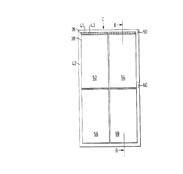
the detector 38. Figure 3A shows a planar view of the tile arrangement (four tiles
in this example, although there will typically be many more tiles in an array). Figure
3B is a cross-sectional view at B-B. Figure 3C is an end view in the direction of the
arrow C.
In Figure 3A, the bonding wires 43 and the stepped uppermost end 50 of the
CA 02260l03 l999-0l-08
WO 98/03011 PCT/EP97/03513
12
uppermost im~ging device tiles 52, 54 (as viewed in Figure 3A) can be seen.
However, the bonding wires 43 and the stepped uppermost end 50 of the lowerrnostimaging device tiles 56, 58 (as viewed in Figure 3A) cannot be seen as these arecovered by the lowermost end 60 of the uppermost imaging device tiles 52, 54 when
S viewed from above (i.e. looking down on the plane of Figure 3A). This is as a result
of the tilting of the signal detecting elements comprising the detector 38 and the
readout chip 39 as can be seen in the cross-sectional view of Figure 3B. In the
particular example shown Figure 3, where the detector 38 and the readout chip 39 are
approximately 18mm by 10mrn, and the tilt provides a difference in the "height" (i.e.
10 the horizontal distance D as viewed in Figure 3B) of the im~ging device over the
support board between the ends of the im~ging device of about lmm, the angle of tilt
of the im~ging device and the im~ging surface is about 3~.
The space between tiles in the direction orthogonal to the tilting direction
(which corresponds the section line B-B) is preferably minimiced by ensuring that the
15 width of the im~ging surface of the detector 38 (i.e. in the horizontal direction as
viewed in Figure 3A) is the same as or greater than that of the readout chip 39 and
the tile PCB 41. In this manner, the tiles can be mounted so that the detectors
actually touch or are separated by a very small amount in that direction.
With an embodiment of this type, the dead space introduced by the bonding
20 pads, bonding wires and readout buffers (decoders, multiplexers etc.) on the readout
chip 39 and the dead space introduced by the tile PCB 41 is elimin~ted because there
is overlap of the total dead region with the (l~tecting element 38 of the previous tile.
Also, there is minim~l or no dead space at all between tiles in the other direction
since tiles are configured to be substantially proximate to or to touch each other and
25 the detector elements 38 may indeed be configured to be precisely equal or extend
slightly beyond the dimensions of the readout chip 39.
While in Figure 3 an arrangement of four tiles is shown it can be appreciated
that any number of tiles can be arranged to provide an im~ging area with any
practically useful size, for example 45cm by 40cm. Also, although in the above
30 described embodiments reference is made to a support plane, this need not in fact be
planar, but could curved or shaped to fit form a desired imaging plane. For example
CA 02260103 1999-01-08
WO 98/03011 PCT/EP97/03513
13
the im~ging support could be shaped as part or the whole of a ring for certain
applications.
The contacts on the imaging support are connected in turn to control
electronics and output electronics for the im~Pin~ array. The output electronics5 include one or more analogue to digital converters for converting analogue signals
from the im~ging devices into digital signals for processing and displaying image
data. An example of suitable control and output electronics and an image processor
is described in the applicant's International patent application WO 95/33332. This
International patent application also described examples of semiconductor pixel
10 irnaging devices suitable for use with the present invention. Thus, the signal
detecting elements referred to above can, for example, be an im~ging device which
provides an array of im~ing cells (or pixels) each including a radiation detector cell
and corresponding charge storage for storing charge directly resulting from radiation
incident on the radiation detector cell, the charge storage of respective im~ging cells
15 being individually addressable for charge readout and/or resetting. However, it
should be noted that im~ing devices other than semiconductor pixel devices may be
used, such as removable CCDs, NaI crystals or small scale wire gas chambers.
An embodiment of the invention thus provides a stationary tiled im~ging area
with minimllm or indeed no dead space at all, this embodiment providin_ tilting of
20 the tiles in the direction of maximum dead space and allowing for overlap between
the detecting element of one tile and the dead area of an adjacent tile. In the other
orthogonal direction, tiles are arranged as proximate to each other as possible or even
touching each other. All tiles are individually removable as previously thus offering
an ideal digital im~ging plane that can be m~int~in~d in parts without compromising
25 the performance.
Although in the embodiment of Figure 3, a wedge-shaped part is shown
between a planar detecting element and a planar PCB mount, it will be appreciated
that alternative constructions may be employed to provide the angled arrangements
of the im~ging surface of the detecting element. For example, blocks along one edge,
30 rather than a wedge-shaped part may be used. Also, the im~gJing device or the mount
may be wedge shaped, or provided with integral supports at one edge for an angled
. . . ~, . . . ~
CA 02260103 1999-01-08
WO 98/03011 PCT/EP97/03513
14
mounting. Alternatively, the mounting locations of the im~ging support could be
angled (tilted), or wedge-shaped, at each mounting location for the im~ging devices
to provide the angled and overlapping mounting of those devices.
Using an embodiment of the invention, for example with the mounting
5 techniques described above, it is possible to configure a variety of clinical equipment
with the im~ging supports ready and mounted on the corresponding systems awaiting
for the im:lging devices. Tm~ging devices can be properly packaged and supplied
separately from the rest of the inl~ging system and any average technical employee
can handle them and relocate them from one plane to another. In this way, the use
10 of the relatively expensive pixel semiconductor im~ginl~ devices is optimized by
requiring less im~ging devices than are needed simult~nPously to equip all systems.
In addition, maintenance becomes cost effective. A defective im~ging device can be
substituted rather than the whole im~ging surface (mosaic) and this can be done easily
by an average technical employee.
The removable securing can be achieved in a non-destructive way such that
an imaging devices may be secured to and removed from an imaging support a
plurality of times leaving the im~ging device, the board(s) and corresponding contacts
in substantially the same state.
The removable mounting may be achieved using alternative techniques
including:
- reduced air pressure, or vacuum as described above, whereby the im~ging
devices are such into position;
- screws glued to the PCBs or other mounting means of the im~ging devices
and then pushed through corresponding holes in the support plane (e.g. the circuit
board of the imaging support), the screws being then secured by nuts on the opposite
side of the support plane;
- a socket configuration (preferably zero-insertion force socket means)
whereby the im~sJing devices have pins that plug into corresponding sockets on the
support plane;
- clips, whereby the imaging devices are kept in position with mechanical
clips, strings or the like;
CA 02260103 1999-01-08
WO 98/03011 PCT/EP97/03513
- magnets, whereby small magnets, either on the im~ging support or on the
im~ging devices, or both, secure the im~sging devices to the im~ging plane;
- other mechanical arrangements.
The invention can be used for any radiation type in any radiation imaging field
5 where areas larger than a few square mm are needed. In particular it finds
application in medical diagnosis im~ginSJ with X-rays and gamma-rays, in
biotechnology imaging with beta-rays (where isotopes are used as labels on the
samples to be image) and in industrial applications for non-destructive tesling and
product quality control.
While specific embodiments have been described, it is to be understood that
many modifications and alternatives can be made without departing from the
invention.
For example, in the embodiment described with reference to Figure 3, the tiles
are tilted with respect to one axis (one direction) with adjacent rows of tiles being
15 arranged so that the detector areas subst~nti~lly touch each other. However, in an
alternative embodiment, it is possible for the tiles to be tilted with respect to two axes
(i.e. about two orthogonal directions, each parallel a respective side of a square tile
or about a single axis which passes through two opposite corners of a tile) so that
dead regions along two adjacent edges of one tile may be covered by the detector20 im~ging surface of two adjacent tiles which meet at the corner between those adjacent
edges. In order to visualise this embodiment, it is helpful to think of the tiles being
arranged like the scales of a fish or in diamond shapes rather than as a rectangular
array of rows and columns of tiles. In other words, for any one tile, two edges
which have dead spaces either side of a first corner will be lower than the two
25 opposite edges either side of the opposite corner. Thus the dead spaces of the two
lower edges of the tile in question will be covered by the detector imaging surface at
the higher edges of two respective adjacent tiles. Also, the opposite, higher edges
of detector imaging surfaces of the tile in question will overlie part of the dead space
at the edges of two further adjacent tiles. For such an alternative embodiment, it is
30 advantageous for the tiles to be substantially square as opposed to being elongated
rectangles. This embodiment if useful for imaging devices having bond wire
CA 02260103 1999-01-08
WO 98/03011 PCT/EP97/03513
16
connections or other dead spaces along two edges, rather than along a single edge as
in the preferred embodiment of Figure 3.
-