Note: Descriptions are shown in the official language in which they were submitted.
CA 02260229 1999-O1-08
WO 98/52294 PCT1US98/02955
WIDE BAND TRANSMISSION THROUGH WIRE
Background
This invention relates to transmission over metallic wire.
In a Plain Old Telephone System (POTS.) environment, a twisted copper
pair is typically employed to a bandwidth of approximately 4 KHz, but recently
several techniques have been created to increase. the available bandwidth.
These
techniques belong to the group of Digital Subscriber Loop modulation
techniques, commonly abbreviated as DSL, HDSL, SDSL, ADSL, etc. (xDSL,
i o as a group).
ADSL (Asymmetric Digital Subscriber Line) is among the best known
xDSL techniques. Pursuant to a "template" recommended by BELCORE, a low
frequency band from 0 to 40 KHz is assigned to a duplex channel that can be
used for POTS or ISDN service. The remainder of the allowed bandwidth, from
~ 5 40 KHz to 1 MHz, is assigned to a uni-directional channel for wideband
applications. 'The original ADSL embodiment utilized a modulation technique
developed at Bell Laboratories in the 1960's which employs an array of
individual low-rate modulated carriers to convey high-rate information (rather
than one modulated carrier with wide sidebands;i. The technique is
2o computationally intensive so it was basically unused until the advent of
powerful
signal processing ICs which allowed the use of Fast Fourier Transform and
Inverse Fast Fourier Transform signal processors for reception and
transmission,
respectively. The resulting technique was embodied by ANSI in T1.413-1995
and is known as Discrete Multitone Modulation, or DMT.
25 The nominally achievable data rate over the wide bandwidth channel
ranges from 1.5 to 6.1 Mbps. However in practice, over a mufti-pair cable, the
rate is substantially smaller. 'The actual achievable data rates depend on a
number of factors, including the length of the copper line, its wire gauge,
presence of bridged taps, varying humidity, charges in characteristics over
time,
3o and interferences, etc. The interferences come from like signals that are
flowing
CA 02260229 2001-06-12
through adjacent wires of a cable, from external sources that are far-removed,
such
as AM radio transmissions, and from near-by isochronous and asynchronous
traffic. What is known is that the xDSL techniques are poorly adapted to deal
with
such interferences and, therefore, it remains to be seen what actual data rate
is
achievable in an environment of a cable with many wire pairs that carry
isochronous and asynchronous traffic.
Summary of the Invention
The problems of prior art broadband transmissions through metallic wires
have been overcome by shedding the fear of interference from other signals
present
on the wires. This is achieved by realizing that a transmission medium
comprising,
illustratively, a cable of wires that commingle their signals through
interference is
no worse than an air interface. Pursuant to this insight, wideband
communication
through a wire is achieved in the presence of other wideband signals in the
wire or
in adjacent wires by applying a modulation schema, or technique, to the
wideband
communication signal to form a signal that is orthogonal or nearly orthogonal
to all
other signals that are present in the wire, whether directly applied or
electromagnetically induced. In accordance with one illustrated embodiment,
CDMA is the schema employed. That is, CDMA code is applied to the wideband
signal that is to be communicate°d through a given wire, and the code
that is
employed is orthogonal to the C',DMA codes that are applied to other signals
that
flow through the wire or through other wires which are in the neighborhood of
the
wire.
In accordance with one aspect of the present invention there is provided a
method of communicating an information signal through said first wire in
proximity to other wires that carry signals, comprising the steps of: applying
a
modulation technique to the information signal to form a modulated signal,
where
the modulation technique is selected to create a first encoded signal that is
CA 02260229 2001-06-12
2a
orthogonal to signals carried in the other wires; and applying the modulated
signal
to the first wire.
Brief Description of the Drawings
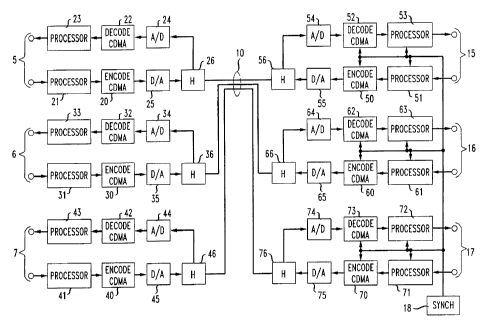
FIG. 1 presents an illustrative block diagram in conformance with the
principles disclosed herein;
FIG. 2 is an illustrative block diagram of functions performed in processor
21;
CA 02260229 1999-O1-08
WO 98/52294 PCT/US98/02955
3
FIG. 3 is an illustrative block diagram ~of functions performed in
processor53;
FIG. 4 presents a conventional embodiment of echo cancellation; and
FIG. 5 presents a reverse-order arrangement of the arrangement shown in
FIG. 1.
Detailed Description
A metallic wire pair attenuates high frequencies and thus acts as a Iow-
pass filter. Additionally, when it is near another wire pair, it couples some
of its
1o signal to the proximate wire by both capacitive; and inductive means. Until
now,
this cross-coupling of signals between wire pairs that are in close coupling
proximity to each other has been considered are evil to be overcome. One
approach that is conventionally used is to twist each of the wire pairs. The
twisting goes a long way toward reducing the interference of an external
signal
on the signal flowing through each twisted pair.
The notion of trying to reduce induced interference from external sources
has been so ingrained in the minds of artisans that no one has stopped to
realize
that a communication channel comprising a caldle of wire pairs, even where
substantial interference is present, is no worse than air; and air is a
2o communication medium that has successfully been used in many applications.
With this insight in mind, we realized tlhat any arrangement where a
signal is modulated so that it is orthogonal to all other signals can be
acceptably
employed in an interference-limited cable. This includes frequency division
multiplexing, time division multiplexing, CDIViA modulation, etc. When two
signals are said to be orthogonal, what is meant is that in the course of
processing one of the signals, the contribution .of the other signal at the
output is
close to zero even when it is present at the input.
FIG. 1 illustrates the contemplated arrangement which, by way of
example, employs CDMA. Element 10 is a cable that comprises a multiple
3o number of wire pairs. Element 21 is a pre-encoding processor that is
responsive
CA 02260229 1999-O1-08
WO 98/52294 PCT/US98/02955
4
to input signals of port 5. The output of element 2 I is applied to CDMA
encoder
20 and, thereafter, to D/A converter 25. The output of converter 25 is applied
to
a wire pair of element 10 via hybrid 26. Signals destined to port 5 arrive at
hybrid 26 and are directed to A/D converter 24. The output of converter 24 is
applied to CDMA decoder 22, and the output of decoder 22 is applied to post-
decoding processor 23. The elements that interface cable 10 to other ports are
illustratively identical to the ones described in connection with port 5, and
bear
correspondingly similar designations.
The signal applied to processor 21 may be an analog signal, or it may be
to a digital signal. If intended to handle analog signals, processor 21
includes an
A/D converter. Typically, the digital signal that is applied to the CDMA
encoder
is not a simple stream of bits (though it could be) but, rather, a steam of
bit
groupings. An illustrative example may be a digital stream that may be created
for a DMT system, and this is illustrated in FIG. 2. Therein, a bit stream is
applied to block l0I which injects error correcting bits (e.g., Reed Solomon
encoder) and the resulting bit stream is divided into groups of bits that are
multiplexed by block 102 to inverse fast Fourier transform (IFFT) processor
103.
In accordance with the teachings of DMT modulation, the number of bits in a
group that is applied to a particular input of the IFFT is a function of the
2o expected signal-to-noise ratio in the frequency sub-channel that
corresponds to
that input (one might choose, for example, 256 sub-channels). The outputs of
the IFFT processor form digitized time samples which are demultiplexed in
parallel-to-serial converter 104 and applied to encoder 20 of FIG. 1.
Encoder 20 encodes, or modulates, the incoming signal (in CDMA, this
is typically referred to as "spreading") with a code C2, and applies the
modulated
signal onto a wire pair of cable 10.
At the receiving end, the signal appearing at decoder 52 is decoded, or
demodulated, (in CDMA, this is typically referred to as "despreading") with
the
aid of code C5, and applied to post-decoding processor 53. Processor 53
3o performs the inverse function of processor 21 and thereby recovers the
signal
CA 02260229 1999-O1-08
WO 98/52294 PCT/US98/02955
sent by port S. When processor 21 has the structure of FIG. 2, processor 53
might be constructed as shown in FIG. 3. Specifically, the incoming signal is
applied to multiplexer 204, the outputs of multiplexer 204 are applied to FFT
processor 203, and the outputs of FFT processor 203 are demulitplexed in
5 parallel-to-serial converter 202. The output o:f converter 202 is applied to
error
correcting block 201 and, thus, the output to port 15 is generated.
The signals of other ports are handled similarly. For example, a signal on
port 16 that is destined to port 6 applies its signal to pre-encoding
processor 61,
encoder 60 spreads the signal with code C62 and applies the signal to a wire
pair
t o that belongs to cable 10.
It may be noted in passing that the apparatus attached to ports 5, 6, and 7
may in some applications be on premises of telecommunication customers, while
the apparatus connected to ports 15, 16, and 1'7 may be on premises of the
telecommunications provider, such as at a central office.
An important aspect of the FIG. I arrmgement is that the encoding
employed in connection with signals flowing in one wire pair is related to the
encoding employed in connection with signals. flowing in adjacent wire pairs
in
such a way that the encoding employed in the one wire pair is insensitive to
signals of the adjacent wire pairs. This insensiitivity may be realized by
various
2o means which can all be encompassed by the notion of orthogonality. In the
FIG.
1 illustration, this is achieved by codes C;~ being mutually orthogonal (where
i=1,2,3,4 and j=1,2) and synchronized to each other. In other embodiments, the
orthogonality can be achieved by time division multiplexing, frequency
division
multiplexing, etc. A mixture is also possible. Viewed another way, all wires
in
cable 10 can carry any and all signals as long as they are modulated to be
mutually orthogonal. This includes, by the wa.y, signals that are injected
directly
into a particular wire pair. Thus, for example, a wire pair can have two CDMA-
modulated signals applied to it, and those signals can be completely separated
from each other and from all other interfering signals as long they are
modulated
3o to be orthogonal to each other.
CA 02260229 1999-O1-08
WO 98/52294 PCT/US98/02955
6
On the other hand, in actual situations of a cable having a number of wire
pairs, not all wire pairs are adjacent to all other wire pairs. Interference
from
adjacent wire pairs may be assumed to be highly objectionable, but it is quite
clear that at some physical separation of wire pairs within the same cable the
interference merely adds to acceptable background noise. Consequently, not ali
of the wires in a cable of wires need to be encoded with mutually orthogonal
modulation signals. A judicious selection of which CDMA code to be used in
connection with which wire in a cable (if CDMA is the schema employed) can
allow one family of mutually orthogonal codes to be used and re-used in a
cable
to that has many more wire pairs than there are members in the code family.
This
is reminiscent of frequency reuse in a cellular telephony environment.
In addition to the fact that not all wire pairs in a large cable need to be
modulated with a mutually orthogonal signal, it should also be realized that
the
orthogonality requirement of this disclosure is, in a sense, quantitative.
That is, a
code pair may be sufficiently orthogonal (to each other) that within the
tolerance
requirements of the system (including, for example, the ability to recover
errors
through the error correction coding) the codes can be considered to be
orthogonal. U.S. Patent 5,461,610 issued October 24, 1995 to Weerackody, for
example, discloses an arrangement where, in an air interface situation, one
can
2o spread signals with codes that have been pre-coded and which are not
completely
orthogonal to each other, and the despreading is performed with the codes that
are not pre-coded.
Hence, in the context of the claims appended hereto, the term
"orthogonal" means "sufficiently orthogonal to create an interfering noise
below
a predetermined threshold."
In applications where ports 15, 16, and 17 are in a common location, the
issue of synchronization is not difficult to resolve. A synch signal source
within
processor 18 in the common location synchronizes all of the local encoders,
and
the only question is how to synchronize the remote encoders. This may be
3o accomplished by processors 51, 61, and 71, under control of processor 18,
CA 02260229 1999-O1-08
WO 98/52294 PCT/US98/02955
moving into a training mode and instructing the remaining processors to
similarly enter a training mode. At that time, a known signal is sent by
processor
51, and decoder 22, for example, adjusts the start of its CDMA code to
maximize
reception of the known signal. Once the start time for decoder 22 is set, the
start
time for encoder 20 is also set. The training mode can be instituted whenever
the
error rate increases above some given thresholld, or at regular intervals, and
the
same procedure applies to all of the remote encoders and decoders. It is
realized
that to the extent that perfect synchronization is not maintained, it is not a
fatal
condition. It merely affects the level of orthogonality.
In connection with the above-mentioned observation that not all wire
pairs in a cable need to have their own CDMA code, it makes sense to make the
selection based on actually measured levels oi' interference. To that end, a
provisioning session is employed, also under control of synch processor 18. In
the provisioning session, synch processor 18 selects a wire pair, selects a
first
15 code of a set of codes, and sets one of the encoders of the selected wire
pair to
that code (e.g., encoder 50). The resulting interference levels (due to
encoder
50) are measured by all of the post-decoding processors (to wit, processors
33,
43, 63 and 73 in FIG. 1 ), and the measured results are sent to synch
processor 18.
When the set of orthogonal CDMA codes consists of N codes, synch processor
20 18 identifies N post-decoding processors with. the highest levels of
interference
(due to the signal of encoder SO}, assigns a different code from the sent of N
codes to the N-1 encoders that are associated 'with the post-decoding
processors
suffering from the highest levels of interference, and repeats the assignment
of
the selected code to the encoder that is associated with the post-decoding
25 processor having the least amount of interference in the group of
identified N
post-decoding processors. The process then repeats until all encoders have an
assigned code.
The code selection process can also bE; carried out on an ad hoc basis,
when a need to assign a code to a wire pair arises. That is, it is quite
possible
3o that not all of the wire pairs in a cable will at any one time be used for
can~ying
CA 02260229 1999-O1-08
WO 98/52294 PCT/US98/02955
8
signals as described herein. At some points, then, a wire pair may be assigned
to
carry such signals and that would call for an assignment of a CDMA code to the
wire pair. Synch processor 18 can observe the cross-talk signals received by
the
wire pair and, through correlation techniques, identify the CDMA code that
presents the least interference. This code can then be selected as the CDMA
code of the wire pair. The above suggests use of synch processor 18, but with
processing power at the terminal ends of the wire pair, it is quite possible
to
assign the task of selecting a CDMA code to the local processor.
In the above description relating to the selection of codes, it may be noted
1 o that when a code was selected for encoder 50, processor 53 was not
mentioned as
being one of the places where the level of interference is measured. That is
not
because it is expected that there would be no interference but, rather,
because it
is expected that this interference can be reduced to a level where it does no
harm.
The interference generated by encoder 50 as measured at processor 53 is due to
impedance mismatches at hybrids 26 and 56. However, the signal being sent to
D/A converter 55 is known and, therefore, it can be subtracted out at the
output
of A/D converter 54. This is a classic echo cancellation problem, and FIG. 4
presents a conventional embodiment for performing that task. It includes an
adjustable finite impulse response (FIR) filter 27 that emulates the echo
paths
(both near-end and far-end), an echo processor 28 that controls filter 27, and
element 29 that subtracts the output of filter 27 from the output of A/D
converter
24. The output of element 29 forms the input to echo processor 28. In
applications where the echo cancellation is effective, the re-use of the CDMA
codes is enhanced because, for example, if interference from a given code used
in encoder 50 is not a problem for decoder 52, then encoder 20 may use the
same
code as is used by encoder 50.
FIG. 1 illustrates an arrangement where processor 21 precedes CDMA
encoder 20. Actually, that is not a requirement, and it is quite feasible to
reverse
the order -- i.e, to have encoder 21 precede processor 20. This is illustrated
in
3o FIG. 5.