Note: Descriptions are shown in the official language in which they were submitted.
CA 022602~ 1999-01-08
WO 98/01979 PCT/US97/11843
ADDRESSABLE, HIGH SPEED COUNTER ARRAY
FIELD OF T~E INVENTION
The present invention relates to telecommunications and
more specifically to high speed network switches.
BACKGROUND OF THE INVENTION
In the management of networks, such as Asynchronous
Transfer Mode (ATM) networks, it is important to maintain
operational and statistical information pertaining to each
of the connections supported by a network switch. In
particular, it is common to keep track of the number of cells
transmitted between addressable nodes, errors, and special
events occurring within the networ~. For example, in the ATM
environment, it is desirable to keep track of the numbers of
cells possessing a cell loss priority of 0 and 1 for each
supported connection. Due to the increasing speeds of
computer networks in the future, it will be increasingly
important to maintain accurate information regarding network
operation to efficiently manage network traffic.
To date, information gathering functions have been
performed on a small scale via the use of discrete counters
or on a larger scale through software. It is possible to
maintain adequate information in networks such as ATM
networks employing DS3 voice carrier systems having a 44.736
megabit per second data rate since at this data rate an ATM
cell is received in approximately 9.47 microseconds (us).
Within this timeframe register updates may be performed in
software or microcode on a serial basis.
Optical carrier links, such as OC-12 and OC-48 however,
have data rates of approximately 622 megabits per second and
2.488 gigabits per second respectively. At the data rate
associated with an OC-12 communication link, an ATM cell
would be received in approximately 681 nanoseconds (ns). At
the data rate aqsociated with an OC-48 communication link,
an ATM cell would be received in approximately 177
CA 02260255 1999-01-08
WO98/01979 PCT~S97t11~3
nanoseconds (ns). Assuming further that it was desirable to
maintain a register for each connection on eight different
types information, it would be necessary to update a register
in approximately 85 ns if the registers were serially
processed in an OC-12 environment and in 22 ns if the
registers were serially processed in an OC-48 environment.
In such communication environments, using the presently known
techni~ues, it would not be possible to maintain desired
operational and statistical information on received cells or
frames.
SUMMARY OF THE INVENTION
In accordance with the present invention a method and
apparatus are disclosed for maintaining information
pertaining to cells received at a network switch in a high
speed network. A network array processor is provided which
includes an addressable high speed register array. The
network array processor includes an index register which is
used to store a value identifying one of a plurality of
network connections supported by the network switch. The
addressable high speed register array includes a plurality
of registers R1 through Rn for each supported connection and
a particular plurality of registers is addressed by the value
in the index register. The register array may comprise a
static random access memory array or any other suitable high
speed memory array. Thus, in a network switch supporting
1024 connections and having eight counters per supported
connection, the high speed counter array would include 8192
registers (1024 by 8).
Additionally, the network array processor includes an
operand register which has operand fields ~l through ~n. Each
operand register may contain a value which specifies the
operation to be performed on the respective register R
through R~ specified by the value within the index register.
Operands are provided which permit the clearing of the
respective register, setting of all bits within the selected
CA 022602~ 1999-01-08
WO 9810~979 PCI-/US97/11843
register, incrementing the selected register, decrementing
the selected register or the retention of the same value
within the register.
Each register within the plurality of registers is
designated as containing a particular data type. For
example, one register may be reserved for counting the number
of received cells for a particular connection, another.
register designated for retaining information on the number
of cells received for the respective connection, another for
lo counting errors associated with the connection, another for
counting cells with a cell loss priority of zero (0) received
for the specific connection and another for counting cells
received at the switch which have a cell loss priority of one
(1) or any other information which is deemed worth of
retention for purposes of network management.
Upon receipt of a cell, the cell header is decoded and
the connection identifier associated with the respective cell
is stored in the index register. Additionally, operands are
generated and stored in the respective operand fields ~l
through ~n of the operand register based upon information
derived from or associated with the received cell.
Thereafter, each of the plurality of registers Rl through Rn
for the respective connection is updated in parallel in
accordance with an operand specified in the operand fields
~l through ~n .
In the above-described manner, a large addressable high
speed counter array is provided in which large volumes of
operational information regarding received cells/frames may
be accumulated in real time. The information within such
array may be advantageously used in the network switch to
efficiently manage the network traffic.
Additionally, one or more state values may be provided
in the register array for each supported connection
identifier. The state values may be single or multi bit
values which have corresponding operand fields which provide
at least for the clearing, 9etting or presetting of the
CA 02260255 1999-01-08
WO98/0197g PCT~S97/l1~3
respective state bits. The state values, for example, may
be employed to indicate that the information pertaining to
a particular connection is valid or to maintain any other
state information via the use of the single or multi bit
values in respective state value locations of the register
array.
BRIEF DESCRIPTION OF THE DRAWINGS
The invention will be more fully understood by reference
to the detailed description of the invention in conjunction
with the following drawings of which:
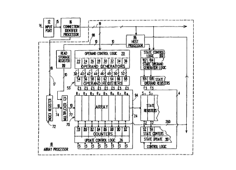
Fig. 1 is a block diagram of a high speed array
processor for maintenance of operational data in accordance
with the present invention; and
Fig. 2 is an alternative embodiment of a h.igh speed
register array for use in the high speed network array
processor of Fig. 1.
DETAILED DESCRIPTION OF THE INVENTION
In accordance with the present invention, a high speed
network array processor is disclosed for maintenance of
statistical and operational information pertaining to traffic
flow within a network switch. More specifically, referring
to Fig. 1, a network switch 10 includes at least one input
2~ port 12 for receiving cells or frames over a communication
link 14. The received cell/frame is passed from the input
port 12 to a connection identifier processor 16 which decodes
header data in the received cell/frame and based upon the
source and destination information contained within the
cell/frame header, generates a connection identifier which
ser~es to uniquely identify the connection within the network
switch lO. Since the universe of possible source and
destination addresses is usually a ~ery large number, network
switches only support a small subset of the possible
connections and the supported connections are dynamically
managed within the switch 10. For example, typical switches
.
CA 022602~ 1999-01-08
WO 98/01979 PCT~S97/11~3
may support lk to 16k connections.
The network switch 10 further includes a high speed
register array processor 18 which is employed for storage of
information pertaining to cells/frames received at the input
port 12. The network array processor 1~ includes operand
control logic 20 which retrieves information from a
respective cell or frame and, in conjunction with operand
generation logic 22, 24, 26, 28, 30, 32, 34 and 36, generates
operands which are forwarded over buses 38, 40, 42, 44,
46,48, 50 and 52 for storage in an operand register 53 having
operand fields ~l through 0~ 54, 56, 58, 60, 62, 64, 66 and
68 respectively. In the presently disclosed embodiment, the
operand buses are three bits wide and the operand fields ~l
through OB are likewise three bits wide thereby allowing for
UP to eight operands. It should be appreciated however, that
a 2 bit operand field may be employed if a smaller number of
operands are used or alternatively, a larger number of bits
may be employed for the operand field if a larger number of
operands must be supported.
A high speed register array 70 comprises a static ram
of sufficient width to accommodate at least eight registers
Rl through R8, each of which is 32 bits in width. The depth
of the array 70 is at least equal to the number of
connections supported by the switch lO which, in the present
exemplary embodiment, comprises 1024 connections. Thus, the
register array 70 is 256 bits wide by 1024 bits in the
present example.
The high speed array processor 18 further includes an
index register 72 which is coupled to a multiplexer 75 via
a bus 74. The output of the multiplexer 75 is coupled to the
address input lines of the array 70 through a bus 77. The
index register is 10 bits wide to accommodate a 10 bit
address value necessary to support 1024 connections and the
buses 74 and 77 are similarly 10 bits wide. The index
register 72 is used to store the value of the connection
identifier. The connection identifier is transmitted from
CA 022602~ 1999-01-08
WO98/01979 PCT~S97/11~3
the index register 72 output to the array address input lines
through the multiplexer 75 and thus selects a plurality of
registers R1 through Ra within the array for a specified
connection.
The network array processor further includes update
control logic 76 and counters Cl through C8 identified herein
as 78, 80, 82, 84, 86, 88, 90 and 92 respectively.
Table I below indicates exemplary operand bit
designations and table II indlcates exemplary types o~ data
for storage within the registers of the array 70.
TABLE I
oPerand Bit Code
Clear ooo
Hold OOl
Increment OlO
Decrement Oll
Set all bits lll
TABLE II
Reqister Data Scored
R1 Cells received
R 2 CLPo
R3 CLP~
R,, CLPo ,
Rs PT~
R6 Congestion
R OAM cell count
As a cell, such as an ATM cell, is received over the
communication link 14 at the lnput port 12 of the network
switch lO, cell header information is forwarded from the
input port 12 to the connection identifier processor 16 over
bus 15 and the connection identifier processor 16 derives a
lO bit connection identifier from the source and destination
address information contained within the cell header. The
CA 022602~ 1999-01-08
WO g8/01979 rCT/US97/11843
lO bit connection identifier is forwarded by the connection
identifier processor 16 over bus 17 for storage in the index
register 72 which comprises a 10 bit register. The output
of the index register 72 is coupled to the address input
lines of the array and serves to select one of 1024 groups
of registers R, through R7 a~sociated with the respective
connection. The cell header for the received cell is also
forwarded from the connection identifier processor 16 to the
operand control logic 20 over bus 19 which, in conjunction
with the operand generators 22, 24, 26, 28, 30, 32, 34 and
36, generates operands employed to control the updating of
the respective registers R, through R8 specified by the
connection identifier stored within the register 72. More
specifically, upon receipt of a cell, the operand control
logic 20 in conjunction with the operand generator 22
generates an operand '010' at the output of the generator 22
and transmits such operand over bus 38 for storage in the
operand field 54 of operand register 53. The operand '010',
as indicated in Table I, indicates that the register Rl is to
be incremented. Additionally, if the received cell contained
a cell loss priority (CLP) bit of '1' indicating that the
cell is subject to being discarded by the network, the
operand control logic 20 in conjunction with the operand
generator 26 would generate an operand '010' which would be
transmitted over the bus 42 for storage in operand field 58
of the operand register 53. Furthermore, since in the
present example, the CLP bit was not a 0, the CLPo register
CA 02260255 1999-01-08
WO 98/01979 PCT/US97/11843
would not be updated. Accordingly, the operand control logic
20 in conjunction with the operand generator 24 would produce
an operand '001' indicating that the value of the register
R2 for the specified connection should be maintained. The
operand is transmitted over the bus 40 for storage in the
operand field 56 of the operand register 53. In a similar
manner, operands are generated and stored in each of the
plurality of operand fields of the operand register 53.
After generation of the operands and storage of the
lo operands in the respective fields 0, through 0~ of the operand
register 53, the operands are transmitted over bus 94 to
update control logic 76. In the present embodiment the bus
94 comprises a 24 bit data bus plus associated control
signals. The contents of the registers R, through R8 for the
connection identified by the connection identifier stored in
the index register 72 are read out of the array 70 and stored
in respective counters Cl through C~ designated herein as 78,
80, 82, 84, 86, 88, go and 92 respectively. Thus, in the
present example, the contents of the register Rl containing
the number of cells received for the connection specified by
the value in the index register would be read and stored in
the counter C~, the contents of the register R2 containing a
value identifying the number of cells received for the
respective connection having a CLP of '0' would be read from
the array and stored in counter C~ and the contents of the
register R3 containing a value identifying the nu~ber of
cells received for the respective connection having a CLP of
-- ,
CA 022602~ 1999-01-08
WO 98/01979 PCTIUS97/11843
'1' would be read from the array and stored in counter C3.
Similarly, the contents of the remaining registers R4 through
R8 would be read from the array 70 and stored in the
respective counters C4 through C8.
The update control logic 76 next causes each of the
counters Cl through Ca to be modified in accordance with the
respective operands. More specifically, the counters Cl
through C8 are updated substantially simultaneously in
accordance with the corresponding operand received over bus
94 at the operand control logic 76. By way of illustration,
in the above referenced example, the counter C1 containing
the received cell count for the respective connection would
be incremented since the operand specified is '010', the
counter C2 containing the number of cells received having a
CLP bit equal to '0' would be unchanged since the operand
specified is '001' and the counter CLP containing the nu~ber
of cells received having a CLP bit equal to 1 would be
incremented since the operand specified is '010'.
After updating of the contents of the counters, the
updated counter contents are written back to the respective
registers R, through R8 of the array 70 specified by the index
register 72.
In the above described manner, statistical and
operational information pertaining to network switch traffic
may be accurately maintained even when cells are received at
622 megabits per second data rate or above.
The data stored in the hi~h speed register array 70 may
CA 02260255 1999-01-08
WO98/01979 PCT~S97/11843
- 10 -
be read out of the array, which in Fig. l is depicted as a
single port random acce~s memory. When it is desired to read
data out of the register array, a host processor 96 transmits
an address to the read 5torage register 99 via bus 98. The
output of the read storage register 99 is coupled to the
multiplexer 75 through a bus 97 and the output of the
multiplexer 75 is coupled to the address input lines of the
array 70 through the multiplexer output bus 77. Data stored
in the registers R, through RB may be read out in parallel
substantially simultaneously so that an accurate picture of
the data stored within the register for a given connection
may be obtained at a given instant in time. It is noted that
if the data within the array is read out of the various
registers sequentially, the data within some of the registers
may have changed due to the receipt of subsequent cells by
the time all of the register contents have been read.
Alternatively, to minimize the width of the data output
interface of the array 70, the data stored in array 70 may
be read out, for example, in successive read operations. In
the first read operation, the least slgnificant byte of each
of the registers R1 through R~ is accessed and in three
additional read operations the more significant bytes of the
respective registers are accessed. In such manner, the width
of the output bus is reduced fourfold. Since the great
majority of changes to the registers are likely to be found
in the least significant byte, most changes to the registers
may be observed without access to the more significant bytes.
CA 022602~ 1999-01-08
WO 98/01979 rCT/US97/11843
The more significant bytes may be accessed upon recognition
that a register has been incremented and that the lncremented
has effected the register across a byte boundary.
To facilitate data read out from the high speed register
array 70 without impacting the updating of the array, the
array may be provided as a dual ported array. In such event,
the address bus 97 is coupled to one set of address input
lines of the array 70 to specify one set of registers for a
read access and the address bus 74 is coupled to a second set
lo of address input lines of the array 70 to specify a second
set of registers for updating within the array.
In addition to the registers Rl through ~, the network
array processor may include one or more state registers Sl
through Sn for each of the connections supported by the
switch. To permit setting and resetting of the state
registers, the array processor 18 includes state control
logic 100 and state operand generator logic 102, 104, etc.
for generating, in the present example, at least two operands
which are transmitted over re~pective bu9es and stored in
state operand registers 106 and 108. In the preferred
embodiment, the state registers S1, S2, etc. are single bit
registers for storage of indicators. For exa~ple, the state
register S1 may contain a valid indicator bit to denote that
~ the data for the respective connection is valid and may be
used. (fill in other indicators that might be used).
Alternatively, the state registers S1, S2, etc. may comprise
multi-bit registers if further granularity to operational
CA 02260255 1999-01-08
WO98~1979 PCT~S97111843
state information within the network switch is desired.
The array processor 18 further includes state update
control logic llO and state counters or update registers 112,
114 for receiving information read out of the state registers
in the event that the registers Sl and S2 are to be modified
through a read- modify-write cycle. ~t should be appreciated
that if the state registers Sl and S2 are merely intended to
set or reset, the state llO, 112 may be dispensed with.
The state registers Sl, S2, etc. may be provided as an
extension of the array 70 and stored in a common static ram
array or alternatively, be stored in a separate random access
memory. In either event the array 70 and the state register
array are indexed by the value of the connection identifier
contained in index register 72 so that all contents of the
registers for a particular connection as well as state
information for a particular connection may be simultaneously
accessed.
An alternative embodiment of the present invention is
illustrated in Fig. 2 in which the array comprises an array
of counters. While more complex, the embodiment of Fig. 2
permits faster update of the contents of the registers and
thus, use of the presently disclosed technique to store
information associated with cells received a~ higher
communication link data rates than would be achievable with
the Fig. 1 embodiment.
More specifically, referring to Fig. 2, the network
array processor include9 an index register 116 which receives
CA 022602~ 1999-01-08
WO 98/01979 rCI'/US97/11843
- 13 -
a connection identifier in the manner hereinabove described
with respect to Fig. 1. The lndex register 116 is employed
to select a plurality of counters Cl through Cn within a
counter array 118 corresponding to counters for the specified
connection. The index regi9ter 116 also addresses state
registers Sl and S2 associated with a specific connection.
Operands are generated in the manner hereinabove
described with respect to operand control logic 20 and
operand generators 22, 24, 26, 28, 30, 32, 34 and 36 and are
stored in operand storage register 120 which includes operand
storage fields OS, through OS8 identified herein as fields
122, 124, 126, 12~, 130, 132, 134 and 136. Each of the
counters C1 through C8 is updated substantially simultaneously
based upon the operand specified in the respective operand
storage field of the operand storage register 120. As a
consequence of the fact that the array 118 comprises a
counter array the selected plurality of counters for a
specific connection may be directly updated without the
delays introduced via the read-modify-write cycle employed
in the embodiment of Fig. 1. Thus, the Fig. 2 array
embodiment may be utilized in conjunction with faster
communication links than are realizable with the embodiment
of Fig. 1.
While the presently disclosed network array processor
has been primarily discussed with regard to use in an
Asynchronous Transfer Mode switch, it is appreciated that
such processor may be employed in any communication switch
CA 02260255 1999-01-08
WO 98/01979 PCT/US9~/11843
- 14
and with any protocol where it is desirable to maintain
operational data pertaining to received cells, packets or
frames.
The above described methodg and apparatus are
illustrative of a novel array processor which permits
maintenance of statistical and operational information
regarding cell/traffic flow in a network switch at extremely
high cell rates. Other modifications, embodiments and
departures from the present disclosure will be apparent to
those skilled in the art without departing from the inventive
concepts contained herein. Accordingly, the invention is to
be viewed as embracing each and every novel feature and novel
combination of features present in or possessed by the
techniques and apparatus herein disclosed and is to be viewed
as limited solely by the scope and spirit of the appended
claims.