Note: Descriptions are shown in the official language in which they were submitted.
CA 02260407 1999-02-12
1
TRANSITION FROM A MICROSTRIP LINE TO A WAVEGUIDE AND
USE OF SUCH A TRANSITION
The invention is based on a transition from a microstrip
line to a waveguide as well as on the use of such a
transition in accordance with the class of the independent
claims.
DE 1 96 14 286 discloses a coupling arrangement for
coupling a resonator to a connecting lead suitable, iri
particular, for use with very high frequencies. A flat
dielectric substrate is thereby aligned with the substrate
plane perpendicular to the wall surfaces of the resonator.
The planar waveguides extending on the substrate, which are
based on microstrip technology, are brought up to the
substrate edge facing the wall surface. The waveguides are
connected, for example, to an extremely high frequency
circuit arrangement. The electric wave field of the
waveguide forming between the two conductors of the
waveguide couples directly onto the electric field of the
resonator in the aperture openings. It is furthermore known
from prior art to couple microstrip lines to antennas. The
microstrip line is carried on a substrate and the energy is
coupled into the radiating antenna via an aperture. The
antenna is designed as a waveguide and is tuned by means of
vapor deposited dielectric films. The energy is coupled
into the antenna through the aperture milled into the base
plate.
CA 02260407 1999-02-12
2
It is furthermore known to produce coaxial connections with
the waveguide by means of coupling rods.
In all cases, tuning is the greatest problem in coupling
microstrip lines to waveguides. Especially in the area of
very high frequencies, the mechanical dimensions of the
components are small and the adjustment by means of tuning
screws required, for example, with the use of coupling
rods, is costly. Tuning by means of fixed dielectric
surfaces in the waveguide is also a costly process.
JP 09246816 (abstract) discloses a transition, which
transmits the energy from the microstrip line to the
waveguide by means of an aperture. The waveguide design is
conventional.
The transition according to the invention with the
characteristic features of the independent claim has the
advantage, by contrast, that it is monolithic, i.e., that
the ground surface of the microstrip line at least
partially forms a wall of the waveguide. The metallic body
is provided with a cutout and a cover. Such a design
permits a stable, robust construction - even for mass-
produced products.
The measures indicated in the subclaims are advantageous
further developments and improvements of the transition
defined in the independent claim.
It is particularly advantageous if the metallic body is
formed by the back cladding of the substrate plate of the
CA 02260407 1999-02-12
3
microstrip line. This permits a particularly simple and
inexpensive design of the transition.
It is particularly advantageous to arrange the aperture
both perpendicularly and parallel to the propagation
direction of the microwaves within the waveguide and thus
to optimize adjustment.
The transition, according to the' invention, makes it
possible in a simple manner to provide means in the
waveguide to effect the adjustment. Suitable are, for'
example, spurs, grooves and similar geometric forms in the
walls.
The adjustment may also be effected by influencing the
microstrip line. Connectable conductor elements, e.g., tabs
bonded to the microstrip line may be used to fine-tune the
component.
Such a component has the advantage of being so robust that
it can be used in a HybridFiber [sic] Radio (HFR) network
for the transmission of high frequency signals.
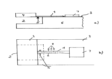
An exemplary embodiment of the invention is depicted in the
drawing and is explained in detail in the description
below. Figure 1a is a cross section of the transition
according to the invention and Figure lb is a top view of
the transition according to the invention.
On a ground surface of a microstrip line (1) is connected
with a monolithic integrated microwave circuit arrangement
CA 02260407 1999-02-12
4
(7). [Grammatically incorrect German sentence.] The
microstrip line (1) is deposited on a dielectric, which in
turn has been deposited on a ground surface (3). A metal
block (6) is provided with a hollow space (2), for example,
milled into the block, which is sealed toward a waveguide
by a cover (4) and by the ground surface (3). A slit-shaped
aperture (5) is made in the ground surface (3).
Using substrate plates with very thick metallic claddings
on their backs makes it possible to form the cutout (2)
directly in the plate. In this case, the upper wall is also
formed by a cover (4). The electromagnetic fields
propagating in the microstrip line (1) are coupled into the
hollow space (2) via the slit-shaped aperture (5) made in
the metallic cladding of substrate (3).
The width and position of the slit in relation to the end
of the waveguide or the microstrip line (1) is to be
selected to achieve the best possible transition.
The best possible transition depends on whether the
microstrip line has an open end or is short-circuited. The
transition in case of an open end is effected by 0/2
adjustment, in case of a short circuit of the microstrip
line by 0/4 adjustment.
Any remaining maladjustment may be reduced, for example, by
adding different conductor elements to the microstrip line
and/or taking measures in the waveguide. For example,
tuning tabs (8) may be bonded to the microstrip line (1)
via wires for adjustment. These tabs and wires may be
already provided during production and connected with the
microstrip line (1) during fine-tuning of the component.
CA 02260407 1999-02-12
For tuning the transition, the waveguide, which is made,
for example, from injection molded aluminum, may also be
given a special form. Platforms or steps may be left in
place to create optimum conditions for adjustment.
Furthermore, adjustment rods for tuning may be provided in
the hollow space. The transition may be effected via the E-
field or the H-field or by a combination of the two.
The microwave printed circuit board (3) and the metal block
(6) may be connected, for example, by a conductive
adhesive.
The transition element according to the invention may be
used, for example, in the area of subscriber lines if
signals in the extremely high frequency range are received
or emitted. The component is used at a base station for a
distribution network and at the subscriber and is a cost-
effective means for rerouting the signals of an amplifier,
which may be integrated, for example, in component 7, to a
waveguide and subsequently to an antenna. The use of a horn
antenna is particularly advantageous for this application.
With such a small, robust component, the last step of
rerouting signals of a base station within a cell of up to
one thousand households, for example, is made possible.
Rerouting to a waveguide permits the use of economically
attractive antennas. The combination of tuning elements in
the hollow space (2) as well as on the microstrip line (1)
allowas for good adjustment of the component to the desired
bandwidth and frequency of the signal. The simple structure
of the component and its monolithic design make it robust
and easy to produce and tune by machine.