Note: Descriptions are shown in the official language in which they were submitted.
CA 02260440 1999-01-28
Doc. No. 70-1 CA Patent
Automatic Focused Ion Beam Imaging System and Method
Field of the Invention
The invention relates to integrated circuit imaging and analysis and more
particularly to the use of focused ion beams for imaging integrated circuits.
Background of the Invention
In the past, reverse engineering of circuits was a straightforward task. A
circuit
board was examined for traces providing a series of conductive connections
between
components. Circuit components were then analysed to determine connected
elements
and finally, a schematic of the board was entered for improvement, re-layout,
or
incorporation into a current design.
With the advent of MSI, LSI, and VLSI, this process became far more tedious.
Initial attempts at reverse engineering integrated circuits relied on visual
images of
integrated circuit layers. Overlapping portions of a layer of an integrated
circuit were
photographed such that a portion of a layer is photographed. The images were
developed
as photographs and the photographs were assembled by hand in order to overlap
adjacent
images appropriately. Because of the redundant nature of integrated circuits,
assembling
the overlapping images into a single large composite image was difficult and
required
some skill.
Once a composite image was formed by taping or gluing the photographs together
in an appropriate fashion, analysis of the images began. The analysis was
performed by a
person skilled in the art of reverse engineering or integrated circuit fault
analysis and
includes the steps of determining conductors, transistors, capacitors,
resistors, etc. and
forming a schematic of the circuit in dependence upon the analysis.
Reverse engineering a complex integrated circuit often represents many man
months of effort and requires significant contribution by highly skilled
individuals.
1
CA 02260440 1999-01-28
Doc. No. 70-1 CA Patent
With the miniaturisation of integrated circuits, optical wavelengths become
less
useful for imaging. Current state of the art integrated circuit fabrication
facilities work at
0.25-0.35 microns and are expected to be further miniaturised. At sizes
smaller than
these, optical wavelengths become too large to properly image integrated
circuit
components. In order to overcome this limitation, it has been proposed to use
scanning
electron microscope (SEM) devices; however, with the use of scanning electron
microscopes, new problems arise. Optical imaging captures information of the
outermost
opaque surface and optical transmission presents certain known problems. SEM
devices
image only surface information unless materials of different average atomic
number are
present within the electron beam penetration depth. The topography that is
imaged is the
final result of all the processes that produce changes in height at the
surface such as
oxidation and metallization crossovers. Thus it is difficult to extract
information
unambiguously relating solely to the upper metallization.
It is therefore common to produce images containing a lot of background
information as well as an image of an outermost layer. Many current imaging
techniques
for reverse engineering focus heavily on techniques for processing the
information to
extract foreground information for circuit analysis. At present, human
analysis is the most
effective.
It would be advantageous to automate some of the functions required to reverse
2o engineer or analyse an integrated circuit (IC).
Prior Art
In U.S. Patent 4,623,255 in the name of Suszko and issued on November 18,
1986, a Method of Examining Microcircuit Patterns is disclosed. The method
comprises
the steps of photographing a portion of an IC with dark field illumination and
then
developing the photograph. As described above, the mosaic formed by assembling
photographs is time consuming and requires expertise.
2
CA 02260440 1999-01-28
Doc. No. 70-1 CA Patent
In U.S. Patent 5,086,477 in the name of Yu et al. and issued on February 4,
1992,
an Automated System for Extracting Design and Layout Information from an
Integrated
Circuit is disclosed. The system comprises an image capture means for
capturing a
plurality of images of an IC and a computer for assembling the images into a
large mosaic
by determining image overlap or by extrapolating images to fill gaps between
adjacent
images. Unfortunately, when working with current IC tolerances, gaps between
abutting
images may contain important circuit elements. Further the system taught by Yu
et al.
requires a known element to occur on each of several layers in order to align
image
composites for a multi-layer IC. A skilled worker identifies the known
element. Finding
and identifying such an element on each layer of the IC is often time
consuming. Also,
removing an IC from the imaging system in order to prepare it for imaging
successive
layers, makes aligning successive layers automatically very difficult.
In U.S. Patent 5,191,213 in the name of Ahmed et al. and issued on March 2,
1993, an Integrated Circuit Structure Analysis method and apparatus are
disclosed. An
electron beam is directed toward successive layers of an IC. Some known
problems with
the use of electron beam scanning of IC layers are solved by Ahmed et al.
Filtering of
image data is required to extract foreground data from background data before
analysis is
possible. This is a significant problem. Also, removing an IC from the imaging
system in
order to prepare it for imaging successive layers, makes aligning successive
layers in an
automatic fashion very difficult.
In U.S. Patent 5,694,481 in the name of Lam et al. and issued December 2,
1997,
a system for automatically constructing a mosaic of images using polygon
extraction and
filtering of images is disclosed. The method appears useful for extracting
circuit
information from SEM image data. The method disclosed deals mostly with the
issues of
filtering and mosaicing of filtered images. The step of filtering to extract
foreground
information from background and foreground information is very time consuming
because of the size and resolution of the images captured. It would be
advantageous to
eliminate this step, but unfortunately, using SEM devices automated circuit
extraction is
not currently possible absent complex filtering of image data.
3
CA 02260440 1999-01-28
Doc. No. 70-1 CA Patent
Focused ion beam (FIB) systems are known for use in several applications. FIBS
are useful in micromachining, imaging and etching. The use of FIBS in imaging
is well
documented. In imaging, an ion beam is focused toward a location and
backscattered ions
are detected. Other particle emissions caused by collisions between ions
within the beam
and a surface being imaged are also detected. Analysis of the detected
particles results in
an image. FIB systems are also used in etching. Etching with FIBS began with
applications for cutting traces in integrated circuits to allow for IC repair.
With gas
assisted etching, FIB systems provide a convenient system for etching away
selected
material from a surface of an IC in order to form holes of a desired depth.
Gas assisted etching is performed as follows. A reactive gas such as chlorine
is
fed into the FIBS near a surface of a substrate. The gas adsorbs to the
surface
approximating a monolayer. When the surface is scanned with ion beams, the
energy of
the ion beams is used to break chemical bonds, thus causing chemical reactions
to
proceed. As well as providing the energy needed to break bonds, the ions
supply
momentum to sputter the substrate. The chemical etching helps to enhance the
physical
sputtering of the ion beam. Another benefit is that the sputtered particles
are volatilised
and pumped away by a vacuum system forming part of the FIBS.
Use of correct etchant gas significantly increases etching rate over FIB
etching
without an etchant gas. The increased etching rate is material dependent so
selection of a
gas for a particular material results in improved etching performance and
improved
control because of etching rate decreases when different material is exposed.
These two
advantages to gas assisted etching are known to allow etching of deep narrow
holes.
In U.S. Patent 5,561,293 in the name of Peng et al. and issued on October 1,
1996,
a Method of Failure Analysis with CAD Layout Navigation and FIB/SEM Inspection
is
disclosed. The method incorporates a dual beam scan of a problem area of a
failed IC to
detect an error in the IC. When no error is detected, layers are etched away
to search for
the error in other layers. The method disclosed by Peng et al. is applicable
to detecting an
error in a known or estimated location but on an unknown layer. Examples of
errors of
4
CA 02260440 1999-01-28
Doc. No. 70-1 CA Patent
this type are hot spots or burns on the IC surface. The general location of
the hot spot is
known but the heat source depth or differently stated the layer generating the
heat is
unknown. The method described by Peng et al. is very useful for analysing IC
failure.
Unfortunately, it is not well suited to reverse engineering because it does
not image entire
layers within an IC nor does it align different layers within an IC. Further,
circuit
information extraction from image data is not taught. Using such a disclosure,
little
regarding reverse engineering of integrated circuits is learned.
Essentially, since a location of the error is known or estimated, the
advantage to
viewing and etching using a focused ion beam is convenience and time. The
disclosure of
using the focused ion beam to etch away material, discloses a known technique.
The
invention directs itself to CAD navigation with error inspection.
Unfortunately, due to the
fine tolerances in present day ICs, it is impossible to accurately re-align
the imaging
apparatus for successive layers when, as stated in the disclosure of Peng et
al. "the sample
is returned to the inspection tool." For the inspection application of Peng et
al., the hot
spot provides a rough idea as to error location, so exact alignment between
layers is
inessential. However, for imaging of an entire IC, exact alignment between
layers is an
important aspect of the reverse engineering process.
In the past, research and expertise has been devoted to filtering images and
mosaicing them to form a single composite image of an integrated circuit
layer.
Unfortunately, the approaches presented heretofore, suffer from significant
drawbacks.
First, filtering is often imprecise and results in errors, which propagate
through to circuit
analysis. Second, the time required to filter and mosaic a composite image is
extraordinary because of the large amount of images captured of each layer.
Third, there
is no method for correcting images of poor quality other than recapturing the
images
using a different sample, which may be difficult to obtain. Fourth, mosaicing
of a
composite image is not a straightforward task due to stage imprecision,
circuit
redundancy, and vast areas (when magnified) of unused circuit space. Many
other
disadvantages of the prior art exist.
5
CA 02260440 1999-01-28
Doc. No. 70-1 CA Patent
The filtering of image data and/or composite images presents the single
greatest
challenge in the field of automated reverse engineering. It is difficult to
extract
foreground data from background data in a robust fashion. Also, because of the
time
requirements, significant delay and cost increases are experienced to analyse
each
integrated circuit device. Often a small portion of an integrated circuit is
analysed to save
time and money. Unfortunately, returning for further analysis requires another
sample.
It would be advantageous to provide a method of imaging an integrated circuit
that does not have these and other limitations.
Summary of the Invention
In accordance with the invention there is provided a method of imaging an
integrated
circuit comprising the steps of:
disposing the integrated circuit on a support for securing the integrated
circuit in fixed
relation to the support; and
iterating the following steps until a predetermined portion of the integrated
circuit is
imaged:
using a focused ion beam imaging system for providing a focused ion beam,
imaging a portion of an outer surface of the integrated circuit by capturing a
plurality of images of different locations on the integrated circuit, relative
motion
between the support and the focused ion beam occurring between image capture
operations, and,
etching a portion of the outer surface from the integrated circuit to expose
material below the outer surface using an etching system, the etching
performed
with the integrated circuit secured in fixed relation to the support.
In an embodiment the method comprises the step of extracting circuit
information from
the composite image absent a step of processing the composite image to extract
foreground information from background information.
6
CA 02260440 1999-01-28
Doc. No. 70-1 CA Patent
In an embodiment the method comprises the steps of filtering the composite
image to
perform one of reducing noise and sharpening edges; and,
extracting circuit information from the composite image, absent a step of
processing
and/or filtering the composite image to extract foreground information from
background
information.
In accordance with another embodiment of the invention, there is provided a
method of
imaging an integrated circuit comprising the steps of:
disposing the integrated circuit on a support for securing the integrated
circuit in fixed
1 o relation to the support;
automatically iterating the following steps until a predetermined portion of
an integrated
circuit is imaged:
using a focused ion beam system for directing a focused ion beam, capturing an
image of a first layer of the integrated circuit and providing a first signal
based on
the captured images;
then providing relative motion between the support and the focused ion beam
the
relative motion provided with the integrated circuit secured in fixed relation
to the
support; and
storing data relating to the captured image and based on the first signal.
In accordance with the invention there is also provided a method of imaging an
integrated
circuit comprising the steps of:
disposing the integrated circuit on a support for securing the integrated
circuit in fixed
relation to the support;
iterating the following steps until a predetermined portion of an integrated
circuit is
imaged:
using a focused ion beam imaging device for providing a beam, capturing a
plurality of images of the integrated circuit from a same relative location
between
the support and the beam, etching of the imaged location of the integrated
circuit
7
CA 02260440 1999-01-28
Doc. No. 70-1 CA Patent
performed between image capture operations, the etching performed with the
integrated circuit secured in fixed relation to the support; and,
providing relative motion between the support and the beam.
Brief Description of the Drawings
An exemplary embodiment of the invention will now be discussed in conjunction
with
the attached drawings in which:
Fig. 1 is a simplified flow diagram of a method according to the prior art of
imaging an
IC using mosaicing;
Fig. 2 is a simplified flow diagram of a method according to the invention of
imaging an
IC using mosaicing;
Fig. 3a is a simplified flow diagram of a method of mosaicing using location
information
provided by a precision stage;
Fig. 3b is a simplified flow diagram of a method of mosaicing using location
information
provided by a precision stage and image correlation;
Fig. 3c is a simplified flow diagram of a method of mosaicing when using
location
information provided by precision markings on the IC;
Fig. 3d is a simplified flow diagram of a method of mosaicing when using
location
information provided by precision markings on the IC and image correlation;
Fig. 3e is a simplified flow diagram of a method of imaging an IC using
mosaicing
wherein information is captured in a redundant fashion to facilitate composite
image
alignment and assembly;
Fig. 4 is a simplified flow diagram of a method of imaging an IC using
mosaicing
wherein image information is analysed to determine required etching and to
enhance
image quality through etching and re-imaging when desirable;
Fig. 5 is a simplified flow diagram of a method of imaging an IC using
mosaicing
wherein information is captured in a redundant fashion to facilitate composite
image
alignment and assembly;
Fig. 6 is a simplified diagram of an IC with part of each of two layers etched
away; and,
8
CA 02260440 1999-01-28
Doc. No. 70-1 CA Patent
Fig. 7 is a simplified diagram of 4 images - two from each of two layers - for
alignment
to form composite images.
Detailed Description of the Invention
Examining and understanding integrated circuits has numerous applications.
Designers often review integrated circuit components of competitive
manufacturers in
order to improve their designs; in patent infringement actions, an explanation
of an ICs
circuitry and mode of operation is sometimes required; and, in reverse
engineering -
copying functionality - of an integrated circuit component, years can be
eliminated from a
design cycle. Current practices, though often significantly faster than an
entire
engineering redesign, are tedious and require significant levels of skill.
In this disclosure and the claims that follow, the following terms are used as
defined here. Plan-view refers to a top-view; a plan view is a view of
substantially a
single layer of an integrated circuit and not a cross section view of an
integrated circuit.
Circuit information refers to information relating to a circuit contained on
the integrated
circuit. Some examples of circuit information include layout information,
circuit
components, circuit interconnects, schematics, netlists, circuit redundancy,
etc. The
phrase "improve imaging results" refers to improving the results of an imaging
step for
use in a further step of analysis. The improvement resulting in an image,
which are
preferred for analysis of circuit information contained within the image
Referring to Fig. 1, a simplified block diagram of prior art reverse
engineering
processes is shown. An imager is used to image a layer of an IC.
Unfortunately, because
of the detail contained in a single IC layer, the imager is capable of imaging
only a small
section of a layer at a time. Further, due to the spacing of traces within an
IC imaging
systems can not image abutting images accurately. A stage is provided for
moving the IC
relative to the imager. A plurality of overlapping images is captured in order
to ensure
that every aspect of the IC layer is imaged.
9
CA 02260440 1999-01-28
Doc. No. 70-1 CA Patent
The captured images are then assembled at an assembly station. An assembly
station often comprises a large table where the images are laid out and
aligned by hand.
Alternatively, current trends toward computer aided design propose that a
computer
algorithm be used to align images and mosaic them into a single final
composite image of
a layer. The composite image is then stored for further analysis.
Unfortunately, due to the
large amount of redundancy in a typical IC, many images are very similar.
Further, due to
the limited information contained within each image frame, automatic alignment
of
images is very difficult. A detailed review of the images and their alignment
is used to
identify mistakes in automatic alignment prior to analysing the composite
image formed.
One common solution proposed in the literature is to provide electronic images
on
a computer and to align these manually aided by image processing algorithms of
the
computer system. Though significant performance improvements are realised, the
system
is not as desirable as one that is truly automated.
Once a layer is imaged, the IC is removed from the imaging station and moved
to
an etching station. At the etching station, a layer of material is removed
from the IC to
expose another layer of circuitry. The IC is then returned to the imaging
station for
imaging of this other layer. Since current IC tolerances are less than a
micron, it is near
impossible to ensure accurate placement and alignment of the IC with each
insertion into
the imaging station. Therefore, a composite image alignment station is
required. At the
composite image alignment station, the composite images are stacked together
and
features on adjacent layers are identified by hand in order to determine inter
layer
connections and inter layer alignment. The resulting three-dimensional
composite image
is analysed to determine a schematic or other representation of the circuitry.
Because the composite images may contain errors of alignment, the alignment of
composite images to form the three-dimensional composite image may also
contain errors
in alignment - the errors propagating. It is desirable to limit alignment
errors in initial
stages in order to improve overall alignment.
CA 02260440 1999-01-28
Doc. No. 70-1 CA Patent
As is evident to those of skill in the art, the above-described method
requires days
or weeks of highly skilled effort. The imaging and etching process requires
significant
human intervention and the resulting data requires a significant amount of
human assisted
interpretation.
As traces on integrated circuits are miniaturised, the limitations of optical
imaging
using conventional microscopes are apparent. Current integrated circuit
spacing is
generally sufficiently large for optical imaging; this will likely be untrue
in a few years.
Throughout the specification and the claims the term capturing an image or
captured image refers to individual images captured by an image capture means.
The term
1 o imaging is used in its general meaning and includes images captured using
scanning
electron microscopes, focused ion beam imaging devices, and other imaging or
sensing
devices which generate image or other sensed data arranged in an array
corresponding to
sensed locations.
Referring to Fig. 2, a simplified flow diagram of a method according to the
present invention is shown. An IC is inserted onto a precision stage for
imaging by a
focused ion beam (FIB) imaging device. Gallium ions are projected toward the
IC
surface. Upon impinging on the IC surface, both ions and electrons are
sputtered off and
electrons are emitted. Some of these sputtered particles are analysed in order
to generate
an image of the IC. In general, information generated based on analysis of
ions which are
sputtered from the surface provides images that are more spatially accurate.
Rendering
electrical charge on the surface of the IC uniform enhances this accuracy. A
known
method of accomplishing this is by flooding the surface with low energy
electrons.
Preferably, the IC is prepared, having a first layer exposed for imaging. The
IC is
secured in place by securing means. Securing means for retaining ICs in place
during
imaging are well known and include gluing, mechanical clamping, etc.
A surface of an exposed layer for imaging is flooded with a low energy
electron
flow. As described above, these electrons help neutralise charge on insulated
portions of
11
CA 02260440 1999-01-28
Doc. No. 70-1 CA Patent
the circuit and, thereby, improve image accuracy and alignment by reducing
image drift.
The FIB imaging device captures an image of a portion of the IC layer by
analysing
sputtered ions therefrom. Alternatively, two images are captured - one of
sputtered ions
while the low energy electron flow is active and one of sputtered electrons
without a low
energy electron flow. A precision stage upon which the IC is mounted is moved
to allow
capturing of another image. Preferably, stage precision is at least as
accurate as minimal
spacing within an IC. The use of an interferometric precision stage as is
available in FIB
systems commercially available from several FIB system manufacturers allows
for such
precision. Preferably precision is better than 50% of a smallest feature size
to be imaged
lo and processed. Preferably, captured images overlap a predetermined amount
in order to
provide a confirmation of stage accuracy. Further images of portions of the IC
layer are
captured until a mosaic of the entire layer can be constructed from the
captured image
data.
When a stage is accurate, image overlap is obviated and image aligrunent is
known. Unfortunately, due to the precision of current ICs, a precision of
better than 0.1
microns is required in an accurate stage in order to allow straightforward
alignment based
on stage positioning and image processing. Because of the redundant nature of
integrated
circuits, precision of better than 1/3 of trace spacing is required in order
provide a truly
indicative estimate of alignment. Image processing is then capable of
deterministically
aligning the images. As is evident to those of skill in the art, at current
rates of progress a
stage having a precision of 0.1 microns is unlikely to remain sufficiently
precise for a
significant length of time. Because of this, it is advantageous to improve
methods of
image alignment in order to maintain current functionality with denser ICs
without
replacing an entire imaging system or precision stage.
Most precision stages are designed to provide precision in a single movement
or a
small group of movements with human operator control. For example, when an
optical
microscope precision stage is designed, its intended use is to allow
navigation to a
location where analysis is necessary. As such, during a single day, the stage
is often only
moved half a dozen times over medium length distances and a few more times
over short
12
CA 02260440 1999-01-28
Doc. No. 70-1 CA Patent
distances. The heat generated is usually very little and the heat dissipates
quickly once
movement is stopped. When heat is generated, temperature rises.
An SEM imaging system uses electromagnetic lenses for focusing the beam. As
such, a stable current is required for good imaging and beam stability.
Temperature,
because it affects resistance, affects current flow and affects image quality.
An FIB
imaging system relies on electrostatic lenses and, therefore, is less affected
by changes in
environmental temperature. For example, heat generated by stage motion and
frequent
movement has little effect on a FIB imaging system. Also, SEM imaging devices
produce
images that vary in rotation depending upon a ration of lens height to sample
height. This
1 o is a result of beam rotation within the magnetic fields generated by the
lenses. The
electrostatic lenses of a FIB do not produce equivalent image rotations
allowing for a
simpler image-processing step for forming a composite image. Simpler
processing steps
save time and often increase reliability. Consequently, in reverse engineering
applications, FIB imaging devices present some significant advantages.
Large depth of field (focus) of an FIB is well known. This large depth of
field
offers significant advantages over optical imaging systems in imaging of
integrated
circuits because a need to refocus the imaging system upon stage movement and
image
blurring due to different distances to the IC surface appearing in a same
image frame are
eliminated. An example of such a difference in distances might occur when
imaging a
transition between the memory array and the peripheral circuitry of a dynamic
random
access memory IC device.
The FIB imaging apparatus is used to etch away material from the exposed IC
layer in a selective fashion. This allows for imaging of subsequent layers in
an automated
fashion without requiring removal and replacement of the IC. Using a precision
stage,
alignment between layers is known within the precision of the stage, because
the IC has
not been moved. Further, by etching only a portion of the exposed layer,
accurate
alignment between layers is ensured using a simple image correlation technique
whether
or not a precision stage is used.
13
CA 02260440 1999-01-28
Doc. No. 70-1 CA Patent
Preferably, some analysis of image data is performed prior to etching away
material. Advantageously, such a process is used to etch small quantities of
material from
portions of an image that are determined to require cleanup. Also, such a
process allows
etching of material in predetermined quantities to confirm analyses, increase
data
quantities, or perform testing. Because the entire imaging, analysis, and
etching process is
performed in situ with minimal or no operator assistance, etching small
amounts of
material wastes far less time than when performed using the prior art method
of removing
the IC, etching the IC, and then replacing the IC. Also, the additional data
determined
through "cleanup" etching improves results of the automatic analysis system
and thereby
reduces a need for human intervention or verification. These advantages and
others are
apparent to those of skill in the art from this disclosure.
Referring to Fig. 3a, the plurality of images are aligned and assembled to
form a
composite image of a layer of the IC. The assembly is performed as follows:
each image
is disposed at its known location as indicated by the precision stage,
redundant image
data in the form of overlapping image portions are discarded. The composite
image is
ready for further analysis. The assembly is performed automatically and
requires no
operator intervention. This is due to the fact that the precision stage allows
for accurate
alignment of even highly redundant circuits.
Referring to Fig. 3b, a method similar to that of Fig. 3a is shown wherein
image
analysis including correlation of overlapping image portions is performed to
improve
alignment beyond the precision of the precision stage. As indicated above,
this method is
preferred to that shown in Fig. 3a because it is applicable to systems having
stages of
lower precision relative to track spacing in the IC. Of course, optionally, a
complete
image mosaicing algorithm relying on precision stage information and image
analysis is
used for forming composite images. Such a mosaicing system will hopefully
extend
imaging system utility to smaller IC spacing than is currently available.
Referring to Fig. 3c, the plurality of images is then assembled into a
composite
image of a layer of the IC. The images are each marked with a location. The
marking is
14
CA 02260440 1999-01-28
Doc. No. 70-1 CA Patent
made on the IC itself to ensure correct alignment. Examples of markings
include overlay
patterns, banding, etched marks within each image, etc. The construction is
performed as
follows: each image is disposed at its known location as determined through
analysis of
the markings, redundant image data is discarded. The composite image is ready
for
further analysis. The assembly of the composite image is performed
automatically and
requires no operator intervention because the markings allows for accurate
alignment of
even highly redundant circuits.
For example, when image distortion is not considered a significant source of
error,
an image is captured, an alignment mark is etched at each corner of the image
of a same
portion of the integrated circuit. An image of a same portion of the
integrated circuit is
captured with the alignment marks. The stage is moved and another image,
overlapping
the first image and including at least one alignment mark and preferably two
such marks
is then captured. Another set of alignment marks is etched. It is apparent
that in
subsequent images only one or two such marks are required depending on how
many
marks is already present in the captured image. For the first image, three
marks are
required. It is evident how to apply such marks depending on an order of image
locations
imaged.
Since each image is captured with and without newly etched marks, no
information is lost and marks are easily used to align captured images having
no new
marks to form a composite image absent marks. Of course, when marks do not
interfere
with analysis, only one image (with marks) is captured at each location. Since
the marks
are etched in situ, the marks are designed for ease of etching identification,
and
alignment. In order to etch using a focused ion beam device, the beam is
maintained in a
single location with a sufficient energy level to etch material from the
integrated circuit
surface. Etching in this manner is known.
Referring to Fig. 3d, a method similar to that of Fig. 3c is shown wherein
image
analysis including correlation of overlapping image portions is performed to
further
improve alignment. Such a system is of particular importance when warp and
distortion
CA 02260440 1999-01-28
Doc. No. 70-1 CA Patent
exist within images. Analysis of image overlap sections allows for reducing
effects of
distortion and warp within the composite image.
For example, referring to Fig. 3e, a composite image of layer 1, the uppermost
layer, is assembled. A substantial portion less than the whole of layer 1 is
etched to reveal
layer 2. A composite image of layer 2 and layer 1 as exposed is assembled. The
remainder of layer 1 is etched to expose the entirety of layer 2. A composite
image of
layer 2 is assembled. It is evident to those of skill in the art that aligning
layers 1 and 2
accurately is greatly facilitated through added correlation information
between the
composite images of layer 1 and layer 2 provided by the composite image of
partial
layerl/layer2. Analysis of traces between layers allows for increased accuracy
of
alignment. Even when layers contain substantially redundant information and
large
unused areas, alignment is likely accurate.
Applying the above method, the composite image of layer 1 is aligned with the
composite image of layer 1/layer 2 by aligning the redundant information. The
redundant
information should align exactly and, when this is not the case, corrections
are applied to
the composite images. Once aligned, layer 1/layer 2 is aligned with layer 2.
Again
misalignments are corrected. When desirable, the process is iterated until no
misalignment occurs. As is evident, since layer 1 and layer 1/layer 2 are
aligned and layer
1/layer 2 and layer 2 are aligned, stacking them and removing the layer
1/layer2 from the
middle results in an accurately aligned layer 1 and layer 2.
Alternatively, following a method according to Fig. 3e, the portion of layer 1
that
is etched comprises a portion of each captured image. This provides increased
information to allow for alignment of every image with an image of another
layer. In use,
such a method provides additional information for mosaicing and for aligning
composite
images. Since, composite image alignment is performed using many correlated
locations,
composite image skew, stretching, or misalignment result in errors in
composite image
alignment. When such errors occur, an error correction algorithm similar to
that described
above is employed to realign images within the composite image.
16
CA 02260440 1999-01-28
Doc. No. 70-1 CA Patent
When a portion of each captured image contains layer 1 and layer 2 information
in
the images captured of layer 1/layer 2, the iterative correction and
realignment algorithm
disclosed above results in a "best" composite three-dimensional image of the
IC. For a
plurality of layers, each intermediate layer - layer n/layer n+1 - provides
alignment
information for each captured image. Each image is aligned using image
analysis to
adjacent images and using the additional information of the intermediate
layer. This
results in a significant ability to correct skew, imaging errors caused by
deflection, and
other causes of misalignment.
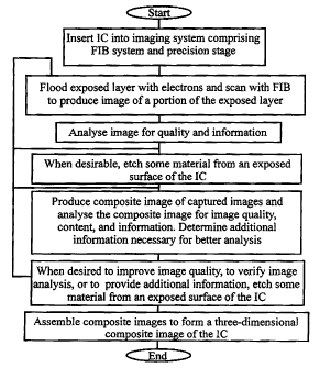
Referring to Fig. 4, another method is shown outlining advantages of the
present
method. A composite image of layer 1, the uppermost layer, is assembled. The
composite
image is analysed. Those areas that are difficult to analyse are recorded, as
are areas
where information below the uppermost layer may be indicative of correct or
incorrect
analysis. Each recorded area is etched for improving the aforementioned
analysis. Images
are captured of the cleaned areas of the IC and are analysed to determine
whether the
newly captured images are of better quality than the previously captured
images. A new
composite image is assembled with those images having a better quality from
the
captured images. Those areas where etching is done to verify the analysis are
imaged and
the analyses are verified. When correct, the system increases its probability
of having
reached an accurate solution. When incorrect, the system attempts to resolve
contradictions or records the possibility of the error and the location for
later review by a
further algorithm or by a human operator. Optionally, the method shown in Fig.
4 is
performed iteratively until the analysis and the composite image are of a
desired quality.
For example, when using a scanning electron microscope system, imaging to a
predetermined depth occurs. When a contact occurs between metal 1 and metal 2,
this is
evident. When using a FIB system, imaging of an external surface is a
straightforward
task, but imaging to a depth beyond the surface is very limited. This is
because ions are
very much larger than electrons and, unlike electrons, do not penetrate
through the
closely spaced atomic layers. They are therefore stopped much nearer the
surface. Upon
analysing an image and determining the presence of a potential metal contact,
etching and
17
CA 02260440 1999-01-28
Doc. No. 70-1 CA Patent
imaging of material below the contact allows for identification of the metal 1
as a contact
with a lower layer or not. In some applications, identification of features
and their
function is the desired end result and, as such, the ability to gather
additional information
through analysis and partial etching of layers is significantly advantageous.
Referring to Fig. 5, a method of mosaicing an entire multi-layered IC
according to
the invention is shown. A FIB is used to image one portion of the IC. A
portion smaller
than the imaged portion is then etched and a same portion is imaged.
Alternatively, a
portion having a same size is etched. The process is repeated for a plurality
of layers. The
precision stage is then moved for imaging the unetched portions. An image of
another
portion of the uppermost layer is captured. This process is repeated until the
entire IC or a
predetermined portion of the IC is imaged. During a processing step, alignment
of
captured images that are in stacked alignment (captured without moving the
stage) is
substantially known because the stage is not moved between imaging of multiple
layers at
a single location. Mosaicing of captured images on a same layer is
accomplished in
dependence upon the plurality of captured images of different layers having
known
spatial relations.
An analogy of alignment of images according to the method of Fig. 5 is
simultaneous equations in mathematics. When an equation has two variables, it
cannot be
solved; another equation is needed. When two adjacent images are aligned,
redundancy
often results in an absence of a single solution. Each layer results in a
number of potential
solutions. By providing additional layers with known relations to existing
layers or each
other, in our analogy, more equations are added to the system. Selecting only
potential
solutions that are substantially common to all layers, a small number of
potential
solutions remain likely. This number is often one but need not be so. Even
when the
solution is not one, other information such as stage precision, even when
using a non-
precision stage, allows for discrimination of a correct solution. Of course, a
precision
stage increases likelihood of correct alignment.
18
CA 02260440 1999-01-28
Doc. No. 70-1 CA Patent
As noted above, as IC trace spacing is decreased, precision stages and imaging
tools become obsolete. The method of Fig. 5 allows for significant extension
of a useful
life of a precision stage by increasing alignment information.
Referring to Fig. 6, a simplified diagram of an IC being imaged is shown. Two
layers are partially etched and a third is being imaged. The images captured
using such a
process are then aligned. The alignment process is explained with reference to
Fig. 7.
Four images are shown in Fig. 7. The upper two images, a and b, are from an
uppermost
layer. The lower two images, c and d, are from a lower layer. The images were
captured
according to the method of Fig. 5. The images of layers c and d are difficult
to align
because lines on those layers are parallel and disposed perpendicular to the
break between
images. That said, the images a and b are easily aligned due to spaces between
parallel
lines. Therefore, layers c and d are aligned because an origin of layer c
corresponds to a
spatial location of an origin of layer a and an origin of layer d corresponds
spatially to an
origin of layer b.
As is well known, gas assisted etching requires selection of an appropriate
gas.
Often, it is desirable to select a gas providing a very fast etching rate on
certain materials
and a relatively slow etching rate on other materials in order to slow the
etching upon
transition to another layer. The selection of gases for this procedure is
usually performed
by FIB operators or other skilled individuals. According to an embodiment of
the
invention, an image is analysed to determine a gas for use in gas assisted
etching. The gas
is selected based on image contrast and identifiable features within the
image. For
example, metal identified within an image is indicative of a metallized layer
and an
appropriate gas is used. The selection of gases based on chemical content is
according to
known gas assisted etching applications. Alternatively, etching the integrated
circuit then
tests the selected gas and verification through imaging or measuring is used
to determine
etch rate. When the etch rate is insufficient, another gas is used and so
forth until an
appropriate gas is selected. Of course, the selection of appropriate gases for
such a system
and image features indicative of a first selected gas or an order of selection
for the gases
is easily determined through experimentation.
19
CA 02260440 1999-01-28
Doc. No. 70-1 CA Patent
It is evident to those of skill in the art that aligning images to form
composite
images of IC layers, analysing images to determine a necessity of cleaning up
an
uppermost layer of an IC being imaged, evaluation of analysis, aligning
composite
images of different layers, and other steps commonly performed by operators of
reverse
engineering equipment require significant time and effort. As a direct result,
an IC may
remain at an imaging station for a prolonged period of time and
simultaneously, imaging
thereof may occupy an experienced reverse engineer's time for a same period or
longer.
According to the prior art, performing all imaging prior to performing
operator-assisted
tasks results in less effective imaging and potentially in loss of
information. It is therefore
1 o undesirable.
According to the present invention, these steps are provided automatically
without
significant operator assistance. Preferably, an IC is inserted into an FIB
system according
to the invention and is checked periodically to ensure correct operation.
Incorrect
operation results, for example, from empty gas supplies when gas assisted
etching is
used, when unresolved errors of significance arise, etc. Other than those
situations
requiring operator assistance, the imaging and composite three-dimensional
image
assembly is conducted unassisted. This reduces human resource requirements and
improves efficiency. Also, the automated FIB system is capable of operating
for a
considerable number of hours more than human engineers over a same period of
time.
Further according to the invention, a step of processing to extract foreground
data
corresponding to an uppermost layer of an integrated circuit from background
data is
obviated. Because a FIB imaging system does not penetrate a sample being
imaged,
resulting images comprises substantially foreground data. Optionally,
filtering to remove
noise and to sharpen edges between features within images is performed.
Processing of
image data is well known in the art of machine vision and it is
straightforward for one of
skill in the art to apply methods of filtering or other processing methods for
image
enhancement to the present application.
CA 02260440 1999-01-28
Doc. No. 70-1 CA Patent
Also, according to the invention, extracted circuit component information is
stored with component location within the integrated circuit in order to
permit association
of circuit components with IC areas - regions - in order to provide schematics
that are
easily associated with the layout. Because circuit layout is often
functionally based, this
often permits reconstruction of schematics into blocks of functionally
associated circuit
elements in a fully automated fashion. It has been found that schematic
generation
according to layout and circuit information results in schematics that are
more easily read.
Further, readability is enhanced by establishing a number of interconnects
between
schematic pages and substantially minimising said number according to any of a
number
of algorithms. One such algorithm is a brute force approach to select a
schematic
pagination that reduces inter-page connections.
The use of a FIB imaging system permits image enhancement through physical
modification of the integrated circuit by etching during imaging thereof.
Prior art systems
and methods do not disclose such an advantage, which is significant because of
increased
efficiency through reduced operator involvement.
Numerous other embodiments are envisioned without departing from the scope or
spirit of the present invention.
21