Note: Descriptions are shown in the official language in which they were submitted.
CA 02260510 1999-O1-28
Doc. No. 70-3 CA Patent
Focused Ion Beam Imaging Method
Field of the Invention
The invention relates to integrated circuit imaging and analysis and more
particularly to the use of focused ion beams for imaging doped layers of
integrated
circuits.
Background of the Invention
In the past, reverse engineering of circuits was a straightforward task. A
circuit
board was examined for traces providing a series of conductive connections
between
components. Circuit components were then analysed to determine connected
elements
t o and finally, a schematic of the board was entered for improvement, re-
layout, or
incorporation into a current design.
With the advent of MSI, LSI, and VLSI, this process became far more tedious.
Initial attempts at reverse engineering integrated circuits relied on visual
images of
integrated circuit layers. Overlapping portions of a layer of an integrated
circuit were
15 photographed such that a portion of the layer is photographed. The images
were
developed as photographs and the photographs were assembled by hand in order
to
overlap adjacent images appropriately. Because of the redundant nature of
integrated
circuits, assembling the overlapping images into a single large composite
image was
difficult and required some skill.
2o Once a composite image was formed by taping or gluing the photographs
together
in an appropriate fashion, analysis of the images began. The analysis was
performed by a
skilled person in the art of reverse engineering or integrated circuit fault
analysis who
performs the steps of determining conductors, transistors, capacitors,
resistors, etc. and
forming a schematic of the circuit in dependence upon the analysis.
Unfortunately, it is
25 not possible, using conventional optics, to image a doped substrate and
thereby to extract
schematic information relating to doped areas. Firstly, imaged features are
commonly
very small and optical wavelengths do not provide sufficient resolution.
Secondly, a
CA 02260510 1999-O1-28
Doc. No. 70-3 CA Patent
substrate, when optically imaged, appears substantially heterogeneous because
doped
areas are substantially different electrically, but are still formed of
substrate material.
Reverse engineering a complex integrated circuit often represents several man
months of effort and requires significant contribution by highly skilled
individuals.
Extraction of dopant related information requires skilled individuals to
analyse layers
adjacent doped layers in order to infer doped layer contents. In essence,
skilled
individuals reconstruct layout information based on contents of other layers.
Even though
this approach is currently acceptable, it is very costly due to the time and
effort required.
For example, a single integrated circuit may comprise l0,000 images for a
single layer.
o To analyse and infer doped regions for each image is a very time consuming
process.
It would be advantageous to automate some of the functions required to reverse
engineer or analyse doped layers within an integrated circuit (IC).
Prior Art
In U.S. Patent 4,623,255 in the name of Suszko and issued on November 18,
1986, a Method of Examining Microcircuit Patterns is disclosed. The method
comprises
the steps of photographing a portion of an IC with dark field illumination and
then
developing the photograph. As described above, the mosaic formed by assembling
photographs is time consuming and requires significant expertise.
In U.S. Patent 5,086,477 in the name of Yu et al. and issued on February 4,
l992,
2o an Automated System for Extracting Design and Layout Information from an
Integrated
Circuit is disclosed. The system comprises an image capture means for
capturing a
plurality of images of an IC and a computer for assembling the images into a
large mosaic
by determining image overlap or by extrapolating images to fill gaps between
adjacent
images. Unfortunately, when working with current IC tolerances, gaps between
abutting
images may contain important circuit elements. Further the system taught by Yu
et al.
requires a known element to occur on each of several layers in order to align
image
composites for a multi-layer IC. The known element is identified by a skilled
worker.
CA 02260510 1999-O1-28
Doc. No. 70-3 CA Patent
Finding and identifying such an element on each layer of the IC is often time
consuming.
Also, removing an IC from the imaging system in order to prepare it for
imaging
successive layers, makes aligning successive layers automatically very
difficult.
In U.S. Patent 5,191,2l3 in the name of Ahmed et al. and issued on March 2,
1993, an Integrated Circuit Structure Analysis method and apparatus are
disclosed. An
electron beam is directed toward successive layers of an IC. Some known
problems with
the use of electron beam scanning of IC layers are solved by Ahmed et al. but,
alignment
of multiple IC layers is not disclosed. Also, removing an IC from the imaging
system in
order to prepare it for imaging successive layers, makes aligning successive
layers in an
t o automatic fashion very difficult.
In U.S. Patent 5,694,481 in the name of Lam et al. and issued December 2,
l997,
a system for automatically constructing a mosaic of images using polygon
extraction and
filtering of images is disclosed. The method appears useful for extracting
circuit
information from SEM image data.The method disclosed presents no information
on
imaging a doped layer within an IC. Unfortunately, a skilled individual using
inference
must perform analysis of the doped layers. As such, the analysis is time
consuming.
Focused ion beam (FIB) systems are known for use in several applications. FIB
systems are useful in micromachining, imaging and etching. The use of FIB
systems in
imaging is well documented. In imaging, an ion beam is focused toward a
location and
2o backscattered ions are detected. Other particle emissions caused by
collisions between
ions within the beam and a surface being imaged may also be detected. Analysis
of the
detected particles results in an image. FIB systems are also used in etching.
Etching with
FIB systems began with applications for cutting traces in integrated circuits
to allow for
IC repair. With gas assisted etching, FIB systems provide a convenient system
for etching
2s away selected material from a surface of an IC in order to form holes of a
desired depth.
Gas assisted etching is performed as follows. A reactive gas such as chlorine
is
fed into the FIB system near a surface of a substrate. The gas adsorbs to the
surface
approximating a monolayer. When the surface is scanned with ion beams, the
energy of
CA 02260510 1999-O1-28
Doc. No. 70-3 CA Patent
the ion beams is used to break chemical bonds, thus causing chemical reactions
to
proceed. As well as providing the energy needed to break bonds, the ions
supply
momentum to sputter the substrate. The chemical etching helps to enhance the
physical
sputtering of the ion beam. Another benefit is that the ejected particles are
volatilised and
pumped away by a vacuum system forming part of the FIB systems.
Use of correct etchant gas significantly increases etching rate over FIB
etching
without an etchant gas. The increased etching rate is material dependent so
selection of a
gas for a particular material results in improved etching performance and
improved
control because of etching rate decreases when different material is exposed.
These two
1 o advantages to gas assisted etching are known to allow etching of deep
narrow holes.
In U.S. Patent 5,561,293 in the name of Peng et al. and issued on October 1,
1996,
a Method of Failure Analysis with CAD Layout Navigation and FIB/SEM Inspection
is
disclosed. The method incorporates a dual beam scan of a problem area of a
failed IC to
detect an error in the IC. When no error is detected, layers are etched away
to search for
15 the error in other layers. The method disclosed by Peng et al. is
applicable to detecting an
error in a known or estimated location but on an unknown layer. Examples of
errors of
this type are hot spots or burns on the IC surface. The general location of
the hot spot is
known but the heat source depth or differently stated the layer generating the
heat is
unknown. The method described by Peng et al. is very useful for analysing IC
failure.
2o Unfortunately, it is not well suited to reverse engineering because it does
not image entire
layers within an IC nor does it align different layers within an IC.
Essentially, since a location of the error is known or estimated, the
advantage to
viewing and etching using a focused ion beam is convenience and time. The
disclosure of
using the focused ion beam to etch away material discloses a known technique.
The
25 invention directs itself to CAD navigation with error inspection.
Unfortunately, due to the
fine tolerances in present day ICs, it is difficult if not impossible to
accurately re-align the
imaging apparatus automatically for successive layers when, as stated in the
disclosure of
Peng et al. "the sample is returned to the inspection tool." For the
inspection application
CA 02260510 1999-O1-28
Doc. No. 70-3 CA Patent
of Peng et al., the hot spot provides a rough idea as to error location, so
exact alignment
between layers is inessential. However, for imaging of an entire IC, exact
alignment
between layers is an important aspect of the reverse engineering process.
It would be advantageous to provide a method of imaging a doped layer within
an
integrated circuit to extract geometric information relating to doped regions
within the
layer and to use this information to aid in deducing the component structure.
Summary of the Invention
In accordance with the invention there is provided a method of analysing at
least a
portion of an integrated circuit comprising the steps of:
1 o removing material from the integrated circuit to expose a portion of a
doped substrate;
using a focused ion beam imaging device, acquiring an image of the exposed
portion of
the doped substrate;
analysing the acquired image to automatically determine first areas within the
exposed
portion of the doped substrate and to automatically distinguish between
substantially
15 differently doped first areas; and
in dependence upon the determined areas, providing circuit information
relating to the
doped substrate layer of the integrated circuit.
According to an embodiment of the invention, the circuit information comprises
circuit
20 layout information including location, size, shape and dopant type of the
areas
determined.
In accordance with the invention there is provided a method of analysing at
least a
portion of an integrated circuit comprising the steps of:
25 providing an integrated circuit having a portion of a doped substrate layer
exposed;
using a focused ion beam imaging device, acquiring an image of the exposed
portion of
the doped substrate layer to produce first signals;
storing data in memory, the data based on the first signals;
CA 02260510 1999-O1-28
Doc. No. 70-3 CA Patent
analysing the stored data to determine a location and dopant type of regions
within the
substrate having substantially different dopant types and providing second
signals
relating to the determined locations and dopant types;
storing data based on the second signals in memory.
In accordance with the invention there is provided a method of analysing at
least a
portion of an integrated circuit comprising the steps of:
using a focused ion beam imaging system, acquiring an image of the exposed
portion of
the doped substrate; and,
1 o analysing the acquired image to automatically determine first areas within
the exposed
portion of the doped substrate and to automatically distinguish between
substantially
differently doped first areas.
Advantageously, a method according to the present invention allows for imaging
of
doped regions within a doped layer of an integrated circuit in order to
extract accurate
dopant type and dopant area geometry information.
Brief Description of the Drawings
An exemplary embodiment of the invention will now be discussed in conjunction
with
the attached drawings in which:
2o Fig. I is a simplified flow diagram of a method according to the prior art
of imaging an
IC using mosaicing;
Fig. 2 is a simplified flow diagram of a method according to the invention of
imaging an
IC using mosaicing;
Fig. 3 is a simplified flow diagram of a method of imaging an IC using
alternating steps
of imaging and etching to facilitate composite image alignment and assembly;
and,
Fig. 4 is a simplified flow diagram of a method of imaging a doped layer of an
integrated
circuit according to the invention.
6
CA 02260510 1999-O1-28
Doc. No. 70-3 CA Patent
Detailed Description of the Invention
Examining and understanding integrated circuits (ICs) has numerous
applications.
Designers often review integrated circuit components of competitive
manufacturers in
order to improve their designs; in patent infringement actions, an explanation
of an IC's
circuitry and mode of operation is sometimes required; and, in reverse
engineering -
copying functionality - of an integrated circuit component, years can be
eliminated from a
design cycle. Current practices, though often significantly faster than an
entire
engineering redesign, are tedious and require significant levels of skill.
Referring to Fig. 1, a simplified block diagram of prior art reverse
engineering
o processes is shown. An imager is used to image a layer of an IC.
Unfortunately, because
of the detail contained in a single IC layer, the imager is capable of imaging
only a small
section of a layer at a time. Further, due to the spacing of traces within an
IC, imaging
systems can not image abutting images accurately without a large potential for
error.
Therefore, a stage is provided for moving the IC relative to the imager. A
plurality of
15 images is captured in order to ensure that the entire area of a desired
portion of the IC
layer is imaged.
The images are then assembled at an assembly station. An assembly station
often
comprises a large table where the images are laid out and aligned by hand.
Alternatively,
current trends toward computer aided design propose that a computer algorithm
be used
2o to align images and mosaic them into a single final composite image of a
layer. The
composite image is then stored for further analysis. Unfortunately, due to the
large
amount of redundancy in a typical IC and the limited information contained
within each
image frame, automatic alignment of images is very difficult and a detailed
review of the
images and their alignment is necessary prior to analysing the composite image
formed.
25 One common solution proposed in the literature is to provide electronic
images on
a computer and to align these manually, aided by image processing algorithms
of the
computer system. Though such a system may realise significant performance
improvements, the system is not as desirable as one, which is truly automated.
CA 02260510 1999-O1-28
Doc. No. 70-3 CA Patent
Once a layer is imaged, the IC is removed from the imaging station and moved
to
an etching station. At the etching station, a layer of material is removed
from the IC to
expose another layer of circuitry. The IC is then returned to the imaging
station for
imaging of this other layer. Since current IC tolerances are less than a
micron, it is near
impossible to ensure accurate placement and alignment of the IC with each
insertion into
the imaging station. Therefore, a composite image alignment station is
required. At the
composite image alignment station, the composite images are stacked together
and
features on adjacent layers are identified by hand in order to determine inter
layer
connections and inter layer alignment. The resulting three-dimensional
composite image
1 o is analysed to determine a schematic or other representation of the
circuitry.
Because the composite images may contain errors of alignment, the alignment of
composite images to form the three-dimensional composite image may also
contain errors
in alignment - the errors propagating. It is desirable to limit alignment
errors in initial
stages in order to improve overall alignment.
As is evident to those of skill in the art, the above-described method
requires days
or weeks of highly skilled effort. The imaging and etching process requires
significant
human intervention and the resulting data requires a significant amount of
human assisted
interpretation.
As traces on integrated circuits are made smaller, the limitations of optical
2o imaging using conventional microscopes are apparent. Current integrated
circuit spacing
is generally sufficiently large for optical imaging; this will likely be
untrue in a few years.
Throughout the specification and the claims the term capturing an image or
captured image refers to individual images captured by an image capture means.
The term
imaging is used in its general meaning and is not limited to optical imaging.
Also, the
term pixel is used to refer to a single imaged point or location. Such a point
represents a
quantisation of a two dimensional view. For example, a pixel may represent a
circular
region 0.1 micron in diameter.
CA 02260510 1999-O1-28
Doc. No. 70-3 CA Patent
Referring to Fig. 2, a simplified flow diagram of a method according to the
present invention is shown. An IC is inserted onto a precision stage for
imaging by a
focused ion beam (FIB) imaging device. Gallium ions are projected toward the
IC
surface. Upon impinging on the IC surface, both electrons and ions are
ejected. Some of
s these ej ected particles are analysed in order to generate an image of the
IC. In general,
ions ejected from the surface provide relatively accurate spatial location
information. This
accuracy is enhanced by rendering electrical charge on the surface of the IC
uniform. Of
course, electron flooding is obviated when charge is not an issue and is not
used when
electrons are the sputtered particles analysed. A known method of
accomplishing this is
1 o by flooding the surface with low energy electrons.
Preferably, the IC is prepared, having a first layer exposed for imaging. The
IC is
secured in place by securing means. Securing means for retaining ICs in place
during
imaging are well known and include adhesives, mechanical clamping, etc.
A surface of an exposed layer for imaging is flooded with a low energy
electron
15 flow. As described above, these electrons help neutralise charge on
insulated portions of
the circuit and, thereby, improve image accuracy and alignment. The FIB
imaging device
captures an image of a portion of the IC layer. A precision stage upon which
the IC is
mounted is moved to allow capturing of another image. Preferably, stage
precision is at
least as accurate as minimal spacing within an IC. The use of an
interferometric precision
2o stage as is available in an FIB system commercially available from Micrion
Corporation
of Peabody MA allows for such precision. Preferably, captured images overlap a
predetermined amount in order to provide a confirmation of stage accuracy.
Further
images of portions of the IC layer are captured until a mosaic of the entire
layer can be
constructed from the captured image data.
25 When a stage is accurate, image overlap is obviated and image alignment is
known. Unfortunately, due to the precision of current ICs, a precision of
better than 0.1
microns is required of an accurate stage in order to allow straightforward
alignment based
on stage positioning and image processing. Because of the redundant nature of
integrated
9
CA 02260510 1999-O1-28
Doc. No. 70-3 CA Patent
circuits, precision of better than 1 /3 of trace spacing is required in order
to provide a truly
indicative estimate of alignment. Image processing is then capable of
deterministically
aligning the images. As is evident to those of skill in the art, at current
rates of progress a
stage having a precision of 0.1 microns is unlikely to remain sufficiently
precise for a
significant length of time. Because of this, it is advantageous to improve
methods of
processor based image alignment in order to maintain current functionality
with denser
ICs without replacing an entire imaging system or precision stage.
The FIB imaging apparatus is used to etch away material from the exposed IC
layer in a selective fashion. This allows for imaging of subsequent layers in
an automated
1 o fashion without requiring removal and replacement of the IC. For metal
layers, this is a
convenient method of ensuring alignment between layers. Using a precision
stage,
alignment between layers is known within the precision of the stage, because
the IC has
not been moved. Further, by etching only a portion of the exposed layer,
accurate
alignment between layers is ensured using a simple image correlation technique
whether
15 or not a precision stage is used. Alternatively, another form of etching is
used to etch
away material from the integrated circuit such as a conventional buffered
etching
solution.
Preferably, some analysis of image data is performed prior to etching away
material. Advantageously, such a process is used to etch small quantities of
material from
2o portions of an imaged area that are determined to require cleanup. Also,
such a process
allows etching of material in predetermined quantities to confirm analyses,
increase data,
or perform testing. Because the entire imaging, analysis, and etching process
is performed
in situ with minimal or no operator assistance, etching small amounts of
material wastes
far less time than when performed using the prior art method of removing the
IC, etching
25 the IC, and then replacing the IC. Also, the additional data determined
through "cleanup"
etching improves results of the automatic analysis system and thereby reduces
a need for
human intervention or verification. These advantages and others are apparent
to those of
skill in the art from this disclosure.
CA 02260510 1999-O1-28
Doc. No. 70-3 CA Patent
Referring to Fig. 3, a method of mosaicing an entire multi-layered IC
according to
the invention is shown. An FIB is used to image one portion of the IC. A
portion smaller
than the imaged portion is then etched and a same portion is imaged.
Alternatively, a
portion having a same size is etched. The process is repeated for a plurality
of layers. The
precision stage is then moved for imaging the unetched portions. An image of
another
portion of the uppermost layer is captured. This process is repeated until the
entire IC or a
predetermined portion of the IC is imaged. During a processing step, alignment
of
captured images that are in stacked alignment (captured without moving the
stage) is
substantially known because the stage is not moved between imaging of multiple
layers at
1 o a single location. Mosaicing of captured images on a same layer is
accomplished in
dependence upon the plurality of captured images of different layers having
known
spatial relations.
An analogy of alignment of images according to the method of Fig. 3 is
simultaneous equations in mathematics. When an equation has two variables, it
cannot be
solved; another equation is needed. When two adjacent images are aligned,
redundancy
often results in an absence of a single solution. Each layer results in a
number of potential
solutions. By providing additional layers with known relations to existing
layers or each
other, in our analogy, more equations are added to the system. Selecting only
potential
solutions that are substantially common to a11 layers, a small number of
potential
2o solutions remain. This number is often one but need not be so. Even when
there is more
than one potential solution, other information such as stage precision, even
when using a
non-precision stage, allows for discrimination of a correct or "best"
solution. Of course, a
precision stage increases likelihood of correct alignment further.
As noted above, as IC trace spacing is decreased, existing precision stages
and
imaging tools become obsolete. The method of Fig. 3 allows for significant
extension of a
useful life of a precision stage by increasing alignment information. It is
evident to those
of skill in the art that having human operators align images to form composite
images of
IC layers and analyse images to extract circuit information is time consuming.
It is
therefore undesirable.
CA 02260510 1999-O1-28
Doc. No. 70-3 CA Patent
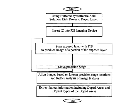
Referring to Fig. 4, a flow diagram of a broad embodiment of the present
invention is shown. A doped substrate layer is exposed through etching of the
integrated
circuit. Preparation of integrated circuits by removing layers is well known.
Commonly, a
buffered hydrofluoric acid solution is used. A traditional buffered
hydrofluoric acid
solution is used to strip down the IC to its substrate layer. According to the
process
carried out during experimentation, extra hydrofluoric acid is added to the
buffered
hydrofluoric acid solution to increase etching rates. Alternatively, a regular
buffered
hydrofluoric acid solution is used. Sometimes metal is not removed by the
solution and
requires physical intervention; for example, brushing the metal with a soft
cloth removes
o it and allows for continued etching. Conventionally, a buffered solution as
disclosed
requires about ten minutes to strip an IC down to its substrate. Preparation
of ICs in this
fashion is known for imaging integrated circuit layers.
Preferably for doped layers, FIB gas assisted etching is not used. This
reduces any
chance that ions used during the etching process implant within the doped
layer, thereby
effecting imaging results. Alternatively, the FIB is used to etch down to a
doped layer
and, when possible, imaging results are analysed in light of the ion
implantation. When
analysis is impossible, a further sample is then prepared using conventional
etching
techniques and that sample is imaged and the images analysed.
Since conventional etching is suggested, alignment between layers is lost
since
2o the IC is removed and replaced or is not a same IC as is used to image
other layers.
Preferably when a same IC is used for imaging each layer, alignment holes are
etched
into the IC to aid in interlayer alignment. Alternatively, bonding pads or
other indicators
of alignment between layers are used. Of course, human assisted alignment of
layers is
also possible.
The etched IC is inserted onto a stage where it is held in position by, for
example,
an adhesive. Methods of retaining an IC stationary during imaging are well
known in the
art and any suitable method may be employed.
12
CA 02260510 1999-O1-28
Doc. No. 70-3 CA Patent
The exposed layer containing doped areas is then imaged using a beam imaging
device in the form of a FIB. A range of FIB imaging energies is applicable and
can be
easily determined through experimentation for providing best image results.
The images
thereby acquired contain significant variation depending on dopant types.
Throughout
s this document and the claims that follow, dopant type is used to denote
neutral or
undoped areas, substantially low concentration dopants, p+ dopants, ri dopants
and other
dopant types. The term dopant type does not refer to specific doping materials
or
substrate materials. Also of note is that a substrate layer that is doped in
some areas is
generally doped across the entire layer or a substantial part thereof and has
areas of
I o different doping existing within the doped layer. Semantically, an image
shows a
distinction between doped regions, rather than showing a distinction between
doped
regions and undoped regions. Alternatively, for polysilicon layers, doped
regions are
surrounded by undoped regions.
Using a scanning electron microscope, images are formed of an exposed surface
15 of an integrated circuit and layers below the exposed surface. Because of
the properties of
a FIB system, only a surface of the integrated circuit is imaged. Therefore
filtering of the
image to remove background information is completely unnecessary. Image
enhancement
is performed to sharpen area borders between adjacent areas having differing
dopant
types or concentrations. A further step of image enhancement to remove noise
and correct
2o for image blur or deformation is also applied. Of course either of these
steps may be
omitted or alternatively, both steps may be performed as a single step.
The image acquired comprises pixels having different intensity levels or
values,
which are easily distinguishable as to dopant type. Areas are extracted from
the enhanced
image and associated with a dopant type for the area. One method of extracting
areas is
25 using polygon extraction. Using polygon extraction, polygons are extracted
representing
each doped area. With each polygon geometry and location, a dopant type is
stored
associated with that polygon. The stored information is useful in extracting
transistor
information from integrated circuits.
13
CA 02260510 1999-O1-28
Doc. No. 70-3 CA Patent
Of course, a method such as that taught by Yu (U.S. Patent 5,086,477) or by
Lam
(U. S. Patent 5,694,48 I ) may be applied to images of different locations on
a same layer.
Application of such a method results in a composite or mosaic image of a
portion of a
layer. Following the mosaicing of the above references or as is known in the
arts of
computer graphics, machine vision, and computer cartography, portions of
different
layers of an integrated circuit are imaged using a FIB system, and a three-
dimensional
image of the layers registered one with another results. Because of the
imaging of the
doped layers as well, the resulting data is particularly useful for reverse
engineering and
integrated circuit analysis.
1 o According to an embodiment of the invention, when a plurality of doped
layers
from a same IC are each imaged according to the invention and then vertically
aligned,
transistor layer layout information including dopant type is automatically
extracted
therefrom. Also in analysis of interconnects effected through connect lines on
polysilicon
layers, dopant types are determinable, whereas prior art methods make
identification of
15 dopant types difficult - requiring significant skill to perform the task.
Further, even with considerable skill reverse engineers often only manage to
correctly determine dopant types of apparent doped regions most of the time.
Errors in a
determination of dopant type, result in flawed schematics. The schematics
require further
analysis, based on functionality, in order to accurately identify dopant types
of doped
20 areas.
According to a further embodiment of the invention, when all layers from a
same
IC are each imaged according to the invention and then vertically aligned,
transistor layer
layout information is automatically extracted and incorporated into schematics
of the
integrated circuit derived through a known circuit extraction method. Examples
of known
2s circuit extraction methods are taught by Yu in the U.S. Patent 5,086,477.
The presence of
information relating to doped regions within the integrated circuit render
circuit
extraction more robust.
14
CA 02260510 1999-O1-28
Doc. No. 70-3 CA Patent
Circuit extraction is a process of extracting circuit information in the form
of
schematic information or layout information. Often, the information need not
be complete
for reverse engineering or circuit analysis. At other times, accuracy and
completeness are
required. According to the invention, more raw data is gathered from an
integrated circuit
allowing for more accurate extraction of circuit data therefrom.
Alternatively, a same
amount of information is extracted using less human intervention and skill.
Component information is a type of circuit information relating to individual
components within a circuit. For example, a transistor location is component
information
as are transistor type, transistor size, transistor gate connections,
capacitor location, etc.
1 o For example, on the lowest doped layer - the substrate - a group of
similarly
doped regions is associated and on an adjacent layer, regions forming the rest
of a
component or a group of components is sought. The regions on the adj acent
layer are
generally proximate the doped regions on the substrate layer. More
specifically, when
two doped areas having n type dopant are located on the substrate layer in
close
t 5 proximity one to the other, then a gate likely exists in a location
between the two areas on
a layer above the substrate. Analysis of the adj acent layer, results in a
located gate and
identification of a transistor, or no located gate and, therefore, no
component
identification.
Components may be identified using a set of rules - for example npn or pnp
2o doped areas. Alternatively, components are identified using templates.
Because of
variations in doped area size, shape and dopant concentrations, a rule-based
approach is
preferred. Those doped areas that are not associated with components are
flagged for
human review and identification or analysis. This reduces missed components or
potential of omission of necessary doped regions in subsequent designs.
25 Even absent automated circuit component extraction, the method of imaging
doped areas is new and provides significant benefits. Heretofore, inference
was used to
extract information relating to doped regions of an integrated circuit.
According to the
CA 02260510 1999-O1-28
Doc. No. 70-3 CA Patent
invention, information is extractable from an IC image itself without
intervention of
highly skilled individuals.
Heretofore, a method of imaging a doped layer of an integrated circuit in plan
view (top view) wherein a distinction between doped regions exists and said
distinction is
sufficient to allow automated extraction of layout information has not been
taught or
proposed. More particularly, prior art methods of imaging an unbiased doped
substrate -
a substrate with no external charge applied - are not known. A method
according to the
invention for imaging a doped layer of an integrated circuit reduces human
resource
requirements and improves efficiency. Also, an automated FIB imaging system
coupled
1 o with an automated circuit analysis system is capable of operating
consistently for a
considerable number of hours more than human engineers over a same period of
time.
Prior art approaches to detecting dopant concentrations in cross section are
mostly
based on human skill. Using a secondary ion mass spectrometry device, there is
a
significant possibility that a dopant will remain undetected due to the very
low
s concentration of dopant material. Using a SEM imaging device, regions of
doped material
are often distinguishable, but concentrations and dopant type are not
distinguishable
without significant skill or analysis using additional complex tools and
techniques.
In an alternative embodiment, the dopant type information is extracted from
cross-
sectional images of a doped device. For example, in order to determine well
geometries
2o and concentrations, an integrated circuit is processed to form a cross-
section thereof. The
cross-section is imaged using a focused ion beam imaging system to produce an
image of
the cross-section. The image - when the cross-section is so chosen - contains
doped areas
that are identified, analysed and a geometry and dopant type of each area is
determined.
Because of the notable difference between n- doping and p+ doping, these are
easily
25 identified. Also, areas doped with lower concentrations are identifiable.
According to an embodiment of the invention, the FIB imaging device is
calibrated to determine intensity regions within captured images indicative of
particular
dopant types including both charge and concentration range. An integrated
circuit is
16
CA 02260510 1999-O1-28
Doc. No. 70-3 CA Patent
imaged and dopant types, their geometries and locations are extracted. This
provides for
automated cross-sectional dopant mapping which has many known applications.
According to another embodiment of the invention, the beam imaging device is a
SEM. The SEM image of the doped layer also has visible distinctions between
differently
doped regions similar to those described above. It has been found that some
applications
are more suited to SEM imaging and others are more suited to FIB imaging.
Numerous other embodiments are envisioned without departing from the scope or
spirit of the present invention.
17