Note: Descriptions are shown in the official language in which they were submitted.
CA 02260719 1999-02-04
Doc No. 79-4 CA Patent
SYSTEM AND METHOD FOR CIPHERING DATA
Field of the Invention
The invention relates to a system for decoding serial data received from a
communication medium. In particular the invention relates to a system for
encoding
and/or decoding of data packets and/or fragments received serially interleaved
one within
another.
Background of the Invention
In the past, security of communications was provided through the use of
encryption technologies. When using encryption, data that is communicated is
first
mapped from its useful state to another obfuscated state wherein it is
inaccessible even if
intercepted. Before being "used," the data is mapped back to its useful state.
Mapping the
data is referred to as encoding and mapping the data back is referred to as
decoding. The
terms encrypting and decrypting, respectively, are also commonly used. There
are many
methods of obfuscating data having varying degrees of security. Some of these
include
DES, triple-DES and CAST. Often, security systems support improvements in the
encoding algorithms used to enable enhanced security algorithms to later be
adopted.
For securing communications, two common models are used, point to point level
security and data level security. In point to point level security, two
endpoints in a
communication medium secure communications therebetween. For example, two
radio
transceivers for use in military applications set up a secure channel, an
agreed upon
encoding/decoding method. All data transmitted is encoded prior to
transmission and all
data is decoded upon receipt. Encoding systems used for data of this type are
usually
optimized for encoding and decoding data within a stream of data. In data
level security,
data is encoded into a file and that file is then transmitted. The received
encoded file is
then decoded to extract the original data. A common form of this type of
encoding system
is Pretty Good Privacy~ (PGP) a commonly available software encryption package
for
personal computers.
CA 02260719 1999-02-04
Doc No. 79-4 CA Patent
A Secure Virtual Private Network (SVPN) is a secure form of a virtual private
network (VPN). A VPN provides an appearance to users of the network of a
physically
connected network of workstations. This appearance is provided even when some
workstations and sub-networks are disposed remotely from the core of the
network. As
such, a person working from home feels as if they are physically coupled to
the network
though they are not. Commonly, VPNs are implemented using a wide area network
such
as the Internet as a communication medium. A workstation is coupled to an
Internet
provider via a modem connection, the core network is coupled to the Internet
through a
gateway and the workstation communicates with the network to provide
functionality as
if a dedicated dial-up connection were made therebetween.
For a user of the workstation, the connection to the Internet and the gateway
is
transparent. Thus, the term virtual in both VPN and SVPN. An SVPN also
comprises
means for securing data transmitted via the Internet to the gateway in order
to prevent
interception and access to sensitive data. Commonly, this means for securing
data
includes a processor for encrypting and decrypting data. Even if intercepted,
the
encrypted data is not accessible.
In order to support data level security of SVPN communication, data is
received
at a gateway and is transferred from gateway memory to working memory where
the data
"pieces" are reassembled to form complete messages and/or transmissions. These
complete messages and/or transmissions are then decoded and the data then
routed within
the private network to a destination. Alternatively, the data is re-encoded
and transmitted
back through the SVPN to the destination. Thus, a gateway has to support
receiving data
within a serial stream, processing the data to determine an associated data
location within
memory, transferring the incoming data to the associated location in memory
and
monitoring memory locations for complete messages that require decoding. This
requires
costly hardware and complicated timing to support memory transfers, serial
data stream
reception and file decoding.
A common approach to securing data is to use a main processor within a gateway
to perform data ciphering operations. Data ciphering includes encoding and
decoding of
2
CA 02260719 1999-02-04
Doc No. 79-4 CA Patent
data. Once data is ciphered, operations relating to data integrity such as
hashing the data
is performed. Data to be transmitted is encrypted and hashed, with hashed data
added to
the encrypted data. Data received is verified and then decrypted.
The processor accesses a memory buffer to read and write data before and after
processing it. Unfortunately, data bus access is a common bottleneck in
processor based
systems. The prior art approach described above requires four memory access
operations
- writing received data to the buffer, reading the data for processing,
writing the data after
processing, and reading the data for forwarding same to a destination. Thus,
even though
a processor is often fast enough to handle the requisite processing, the bus
access limits
the overall efficiency of such a system.
It would be advantageous to simplify the ciphering of data within a serial
data
stream when received by the gateway.
In order to overcome the above limitations of the prior art, it is an object
of the
invention to provide a method of ciphering data received by a gateway, the
data ciphered
absent accessing the memory buffer via the data bus.
It is another object of the invention to provide a method of encoding data for
transmission via a wide area network. the data ciphered and processed for
determining
integrity in parallel.
Summary of the Invention
In accordance with the invention there is provided a system for ciphering data
stored
within a memory buffer comprising:
an integrated processor for retrieving data from the memory buffer, for
ciphering the
data, and for performing operations relating to verification of data
integrity, the ciphering
and the performed operations executed in parallel, the processor for providing
processed
data.
In accordance with the invention there is also provided a system for ciphering
data
comprising:
CA 02260719 1999-02-04
Doc No. 79-4 CA Patent
a memory buffer having a first port and a second port;
a plurality of communication ports;
a first processor in communication with the first port of the memory buffer
and the
plurality of communication ports;
a second processor in communication with the second port of the memory buffer,
the
second processor for ciphering data within the memory buffer and for storing
the data
ciphered data within the memory buffer,
wherein data ciphering operations do not affect operations of the first
processor.
Brief Description of the Drawings
The invention will now be described in conjunction with the following drawings
in which:
Fig. 1 is a simplified block diagram of a prior art ciphering system;
Fig. 2 is a simplified block diagram of a ciphering system according to the
invention;
and,
Fig. 3 is a simplified block diagram of a ciphering processor for use with the
present
invention.
Detailed Description of the Invention
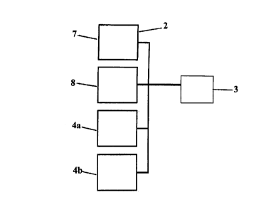
Referring to Fig. 1, a data ciphering system according to the prior art is
shown.
The data is provided as a stream of data values in the form of bits. As shown,
the bits
arrive at a first communication port 4a and are stored in buffer memory 3 via
the data bus
2. A processor 7 determines start locations and end locations of packet
fragments as the
bits are placed within the buffer memory 3. Alternatively, this is done when
bits are
already within the buffer memory 3. Determining packet start, end, and
contents are
known in the art of data communications.
When the beginning of a packet is detected by the processor 7, a new file
within
the memory is created or a new portion of the memory is allocated for the
packet. A
ciphering circuit 8 then retrieves the file from the memory buffer via the
data bus 2. The
data within the buffer memory 3 is ciphered and data integrity information is
generated
4
CA 02260719 1999-02-04
Doc No. 79-4 CA Patent
for data integrity verification. The ciphered data is then stored in the
memory via the data
bus 2. When data is being secured for transmission via a wide area network,
the integrity
information is stored with the ciphered information. The processor 7 then
retrieves the
ciphered information from the memory 3 via the data bus 2 and provides it to
the second
communication port 4b.
From Fig. 1 and the above description, it is evident that at least four data
bus
operations are necessary for each packet. Since data busses often form a
bottleneck in
system performance, the resulting system is often inefficient. Even though,
all processing
of encryption and data integrity is performed by a special processor 8, the
resulting
improvement in system performance is not substantial.
Referring to Fig. 2, a data ciphering system according to the invention is
shown.
The data is provided as a stream of data values in the form of bits. As shown,
the bits
arrive at a first communication port 4a and are stored in buffer memory 5. A
processor 7
determines start locations and end locations of packet fragments as the bits
are placed
within the buffer memory 5. Alternatively, this is done when bits are already
within the
buffer memory 5. Determining packet start, end, and contents are known in the
art of data
communications.
When the beginning of a packet is detected by the processor 7, a new file
within
the memory is created. A ciphering processor 13 then retrieves the file from
the memory
buffer via a second other data bus. The data within the buffer memory 5 is
ciphered and
data integrity information is generated for data integrity verification. The
ciphered data is
then stored. When data is being secured for transmission via a wide area
network, the
integrity information is stored with the ciphered information. The processor 7
then
retrieves the ciphered information and provides it to the second communication
port 4b.
Clearly, processing of a packet requires at least two data bus operations,
half of
the prior art implementation. Thus, using a system as described herein,
performance is
improved substantially. Also, since the ciphering processor operates
independent of the
processor 7 and of the data bus 2, it is possible to clock the ciphering
processor 13
independent of the other processor. Therefore, when ciphering operations prove
to be a
5
CA 02260719 1999-02-04
Doc No. 79-4 CA Patent
bottleneck, a faster ciphering processor is used. Alternatively, when the
processor 7 is the
bottleneck, a faster processor 7 is used.
The memory buffer 5 is preferably formed of dual ported random access memory.
Of course, when reduced performance is acceptable, a random access memory
arbitration
circuit (not shown) is used to arbitrate access to the random access memory
making it
function similarly to dual ported memory. In essence, either the ciphering
processor 13 or
the processor 7 are switched to drive the memory circuitry. By using true dual
ported
random access memory, both the processor 7 and the ciphering processor 13 can
access
the memory 5 simultaneously. This effectively eliminates operations of one
processor
from affecting operation the other.
At least four memory access operations are required to process a packet;
however,
they are now performed two on the data bus and two on a second other data bus.
This is
highly advantageous as described above.
The implementation of ciphering and data integrity operations in parallel
improves system performance. Prior art systems perform one operation and then
the
other, implementation of the two operations in parallel requires some set up
operations
and a final operation of the data integrity processing. That said, it reduces
two sequential
operations to one operation equal to the greater of the two. The improved
efficiency
allows for a ciphering processor 13 having reduced performance and yet capable
of
achieving a same overall data throughput.
Referring to Fig. 3, a block diagram of the ciphering processor 13 is shown.
The
ciphering processor 13 is implemented within programmable logic of a field
programmable gate array (FPGA). The FPGA is in communication with the dual
ported
random access memory 5 and with a command FIFO 15. The ciphering processor 13
comprises four main blocks. The 3-DES core is a ciphering block for performing
encryption and decryption of data according to the DES standard. Of course,
other
methods of data obfuscation may be implemented in conjunction with the DES
core.
Alternatively, another form of encryption is used in place of DES. An SHA-1
block
implements SHA-1 data integrity hashing and verification. The block provides a
signal
6
CA 02260719 1999-02-04
Doc No. 79-4 CA Patent
related to the integrity of data analysed. When data integrity is verified,
that data is
acceptable and the processed packet continues normal processing, otherwise an
error is
indicated and an error handler sends appropriate signals for indicating the
communication
error. An MD5 block performs data integrity hashing and verification according
to MDS.
As used herein the term data integrity hashing is equivalent to message
digesting (MD).
The DES, MDS, and SHA-1 methods are well known in the art.
For example, the Secure Hash Algorithm (SHA), the algorithm specified in the
Secure Hash Standard (SHS, FIPS PUB 180), was developed by NIST. SHA-1 is a
revision to SHA that was published in l994; the revision corrected an
unpublished flaw
in SHA. The design of SHA-1 is very similar to the MD4 family of hash
functions
developed by Rivest. SHA-1 is also described in the ANSI X9.30 (part 2)
standard.
MD2, MD4 and MDS are message-digest algorithms developed by Rivest.
Thus, it is clear that implementation of these functions in parallel within a
single
ciphering processor is advantageous. Further, since the processed data is same
data, the
use of single integrated processor reduces memory access operations since same
data is
used by each of the processing portions of the ciphering processor 13. This
has an added
advantage of increasing performance through reduced access to external memory.
When a packet is ciphered according to the invention and results in a packet
that
is too large for transmission via a network, the packet is fragmented. Such a
packet,
having two fragments. In this case, the receiving end may be optimized to
process paired
fragments.
By performing encryption and integrity encoding in a single pass, very high
speeds are supported efficiently. For example, encryption according to the
IPsec standard
is performed and integrity encoding using message digests is performed. Of
course, very
high speeds can be supported through other architectures.
A hardware implementation of a gateway ciphering system is implemented within
an ASIC or other custom circuitry. Alternatively, a commercially available
processor is
dedicated to performing the ciphering processing. This provides very high
performance
7
CA 02260719 1999-02-04
Doc No. 79-4 CA Patent
and processor independence. In effect, the use of custom circuitry allows for
increased
efficiency in exchange for increased design and implementation costs.
Alternatively, the
hardware is implemented in programmable logic such as a field programmable
gate array
(FPGA).
Advantageously, a hardware implementation as disclosed above offloads much of
the processing requirements for packet processing from a host processor. The
resulting
system has a host processor and a ciphering processor that are relatively
independent.
Unfortunately, a level of independence achieved is generally at an expense of
further
processing ability within the ciphering processor. For example, in order to
cipher a
packet, it is generally required to have a security association for the
packet. In order to
determine the security association, either the ciphering processor is
significantly more
complex or the host processor is used.
Accordingly, an architecture is presented below for providing a balance
between
cost and performance for a ciphering system according to the invention. The
host
processor determines a security association based on a source/destination of a
packet. The
security association and the source/destination in the form of an address are
stored for
access by the ciphering processor. In this fashion, the host processor
determines a
security association for an address once instead of many times. Likewise, the
ciphering
processor is capable of ciphering many packets without further processing by
the host
processor and with little added complexity.
The ciphering system in the form of an ASIC or an FPGA includes means to look
up the security association determined by the host processor. The security
association is,
for example, a the context in which a packet is to be ciphered including keys
and
ciphering algorithms The host processor includes means for determining a
security
association and for storing the determined security association in a location
accessible by
the ciphering processor. For example, the security association is stored in
the dual ported
RAM. Alternatively, the security association is stored in memory within the
ciphering
processor.
8
CA 02260719 1999-02-04
Doc No. 79-4 CA Patent
In use, the ciphering processor receives a packet. An address for the packet
is
determined and a security context associated with the packet address is
located when
present. The located security context is then used to cipher the packet.
Alternatively,
when the security context is not present, a signal is provided to the host
processor which
then determines and stores a security context for the packet. Such a method
shifts much
of the packet processing requirements from the host processor to the ciphering
processor
is an efficient and cost effective manner.
Accordingly, the host processor performs key negotiation and setup. It also
stores
data within a table, which the ciphering processor later references. The
ciphering
processor then processes all subsequent packets in that security context
without
burdening the host processor. Further, since the ciphering processor need only
perform a
lookup for each packet, the complexity of the hardware and per-packet overhead
are both
small.
Numerous other embodiments may be envisaged without departing from the spirit
or scope of the invention.
9