Note: Descriptions are shown in the official language in which they were submitted.
CA 02260839 l999-0l-l8
- W O 9~ U7~ PCT~B97/00903 -
BLIND DFE AND PHASE CORRECTION
S FIELD OF THE INVENTION
The present invention relates to digital communication methods and
systems.
BACKGROUND OF THE INVENTION
Modems for digital communications systems are designed to cope
10 with various channel imp~irments. An essential element of the modem is the
start-up process in which modem parameters such as equalizer taps, carrier
frequency error, timing error, and gain setting, are estimated in order to provide
the required modem perforrnance.
In the prior art, two training modes are used: 1 ) using a known
15 transmitted data sequence; 2) or using the transmitted information data without
any prior knowledge of the value of the transmitted data. The latter mode is
known as a blind start-up.
In the prior art, it is difficult to perform a blind start-up process,
with limited computational resources and to converge to a good initial setting of
20 the modem parameters for channels that exhibit severe linear distortion whichgives rise to severe inter-symbol interference (ISI), and channels that suffer from
severe narrow-band interference.
Therefore, there is a need in the art to provide a solution for the
blind start-up process of a receiver in the context of digital communications
25 signals in the presence of severe ISI and severe narrow-band interference. There
is an additional need in the art to provide relief from ISI and severe narrow-band
interference for conventional blind and non-blind modems.
SUMMARY OF THE INVENTION
The present invention is a method and apparatus for a digital
30 communication receiver which is capable of operating over channels with severe
ISI and narrow-band interference in either blind or non-blind modems.
The receiver of the present invention receives an analog signal
modulated with digital information. The receiver converts the analog signal to adigital signal and demodulates the digital signal to recover the complex valued
CONFIRM~JION COF~
CA 02260839 1999-01-18
~~ wO 9~ ~7~ PcTtIsg7/00903
components of the transmitted digital signal. The complex valued components
are low pass filtered and passed through an adaptive pre-equalizer filter to reduce
eigen value spread correlation.. The filtered complex valued signal is then
subjected to a decision feedback equalizer which operates using a series of
adaptive filters to additionally remove artifacts of inter-symbol interference. The
resulting filtered and equalized complex valued signal is the converted to a
digital signal to recover the digital information.
BRIEF DESCRIPTION OF THE DRAWINGS
Figure 1 depicts a digital communications system which employs
the invention in a preferred embodiment.
Figure 2 describes the transmitter in the preferred embodiment of
Figure 1.
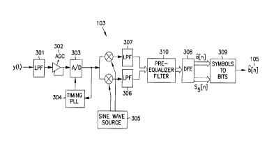
Figure 3 describes the structure of the receiver in the preferred
embodiment.
Figure 4 describes the operation of the pre-equalizer filter unit of
the receiver in the preferred embodiment.
Figure 5 describes operation of the DFE (Decision Feedback
Equalizer) in the receiver of the preferred embodiment.
DETAILED DESCRIPTION OF PREFERRED EMBODIMENTS
In the following detailed description of the preferred
embodiments, reference is made to the accompanying drawings which form a
part hereof, and in which is shown by way of illustration specific preferred
embodiments in which the inventions may be practiced. These embodiments are
described in sufficient detail to enable those skilled in the art to practice the
invention, and it is to be understood that other embodiments may be utilized andthat structural, logical and electrical changes may be made without departing
from the scope of the present inventions. The following detailed description is,therefore, not to be taken in a limiting sense, and the scope of the present
inventions is defined only by the appended claims.
Reference is made to Figure I which illustrates a typical
application of a digital communications system operating over UTP (Unshielded
CA 02260839 1999-01-18
~- W O~ IC7~ PCT~B97/00903 -
Twisted Pair) copper cables plant 102 or another communication medium such
as coaxial cable. The present invention is applicable to many types of
communication mediums, and in particular to a digital subscriber loop of a
telephone network or a coaxial cable television infrastructure. The system
5 comprises a transmitter 101 that receives a sequence 104 of data bits b[n], and
outputs a signal x(t) to the cable. A wired communications medium 102, such as
a copper cable plant, connects the transmitter 101 to the blind receiver 103. The
blind receiver 103 receives a signal y(t) from the communications medium 102
and outputs a sequence of detected digital data bits 6 [n] 105.
The communications medium or cable plant may have one or
more unterminated wire drops 106, as illustrated in Figure 1, and these wire
drops may cause severe reflections that distort the signal and introduce
significant inter-symbol interference (ISI).
Reference is made now to Figure 2, which describes the structure
15 of the transmitter 101. In figure 2, the single-lined arrows indicate the
propagation of real valued signals and the double-lined arrows indicate the
propagation of complex valued signals. Real valued signals are a subset of
complex valued signals and thus whenever the term "complex valued" is used
herein, it encompassed either im~in~ry or real valued signals or the combination20 of the two which is a complex valued signals. The transmitter 101 operates
according to a general approach of linear transmission that particularly includeany one of PAM (Pulse Amplitude Modulation), QAM (Quadature Amplitude
Modulation), PSK (Phase Shift Keying), CAP (Carrierless AM-PM), and NRZ
(Non-Return to Zero) tr~n~mi~ion methods, among others. The input data bits
25 sequence b[n] is converted to a sequence of I-Q complex valued symbols, a[n],by a bit-to-symbol conversion unit 201, that may comprise a scrambler, a
differential encoder, a trellis or a block FEC (Forward Error Correction) encoder,
a CRC error protection encoder, a framer, a shell mapper, and/or protocol layer
units.
The sequence a[n] is then fed to a cascade of tr~n~mi~sion filter
202, an up-converter 203, where it is multiplied by sine and cosine sequences
.
CA 02260839 1999-01-18
~- W O 98~ 7~ PCT~B97/00903 -
that are generated in the sine wave source 204, a Digital to Analog (DtA)
converter 205, an analog LPF (Low Pass Filter) 206 whose cutoff frequency is
designed to reject ~ cing effects of the D/A, and an amplifier 207. The output
of the transmitter is the analog signal x(t).
Reference is now made to Figure 3 which illustrates the structure
of the blind receiver 103. The input to the blind receiver is an analog signal y(t)
that has propagated through the wired communications medium 102, such as a
copper cable plant. This signal may suffer from severe reflections and linear
distortions and it may contain a high level of noise and interference components10 due to e.g. narrow-band radio tr~n.~mi~ions which occupy the same frequency
band of the signal y(t).
The receiver input signal is low-pass filtered by the LPF 301
which is designed to combat sampling ~ in~ effects, then it is amplified by an
amplifier 302 whose gain is automatically adjusted with an Automatic Gain
15 Control (AGC) to exploit the dynamic range of sampler, and then the signal issampled by Analog to Digital converter (A/D) 303. The sampling phase of the
A/D is adaptively controlled by a timing PLL (phase locked loop) 304, which
adjusts the sampling phase so that the power of the A/D output is ma~cimi7e~
Those skilled in the art will readily recognize that the timing PLL 304 may
20 alternatively employ other conventional timing methods, such as decision
directed timing.
The A/D output sequence is then down-converted by multiplying
it with sine and cosine sequences that are synthesi~d in a sine wave source 305,and the resulting I and Q components are low pass filtered by the LPFs 306 and
25 307. Both LPFs 306 and 307 are designed to remove the demodulation image, to
remove out-of-band signals, and to match the response frequency of the ca~ca~le
of the tr~n~mi~ion pulse response of transmit filter 202 of a typical cable plant
or other communication medium 102 upon which the system operates.
The LPF units' outputs are then processed by a pre-equalizer filter
30 unit 310, whose operation is described below in conjunction with Figure 4, and a
Decision Feedback Equalizer (DFE) unit 308, whose operation is described
CA 02260839 1999-01-18
~- W O 98/04073 PCT~B97/00903 -
s
below in conjunction with Figure 5. The output of the DFE unit 308 is a
sequence of detected I-Q symbols â[n] and an equalized sequence s5[n]. These
sequences are then processed by a symbol-to-bits conversion unit 309 that
performs the inverse function of the bits-to-symbols conversion unit 201 and
5 may employ a descrambler, differential decoder, FEC decoders, deframer, shell
demapper, and/or a protocol layer decoder. The output of this unit is a sequenceof the detected data bits 6 [n] 105.
Figure 4 illustrates the pre-equalizer filter unit 310. The input
sequence ofthe unit, s,[n] is filtered by a digital FIR (Finite Impulse Response)
10 filter 401 with L taps Pn[ 1 ]~pn[L] (L 2 0) where p"[l] denotes the l-th tap after n
iterations. The taps of the filter are adaptively adjusted by an adaptation unit402. The adaptation rule is:
Pn+l [l] = Pn[ll + rn (s2[n])sl [n-l~ I = I ... L
where s2[n] is the output of the FIR filter 401, and where rn(x) is a possibly
15 nonlinear function 403 whose parameters may vary with the iteration index n. A
recommended class of r function is:
rn (x) = ~p[n] ~ x
where ~p[n] n - 1,2,... is a sequence of step sizes. The signal undergoes the
following transformation:
L
s2 [n] = sl [n] + ~, pn[l]sl [n-l] (L20)
1=1
The input signal for the pre-equalization filter unit 310 is denoted
sl [n] in Figure 4 and is routed to the FIR filter 401, the adaptation unit 402 and
to sumrnation circuit 404. s, [n] is combined with the output of the adaptive FIR
filter 401 to produce the output signal s2[n] of the pre-equalization filter unit 310.
The non-linear circuit 403 modifies the s2[n] signal to provide the feedback to
adjusting the taps if adaptive FIR filter 401.
Figure 5 illustrates the DFE (Decision Feedback Equalizer). The
DFE's input sequence s2[n] is first rotated by an adaptive rotator 501, by an
CA 02260839 1999-01-18
~~ W 0 98/04073 PCT~B97/00903 -
angle ~[n]. The rotated sequence is then filtered by an FFE (Feed Forward
Equalizer) FIR filter 502 whose taps' values are cn[l]..cn[M~ (M 2 1), to produce
output signal s3[n]. Signal s3[n] is then summed 507 with the output of an
adaptive FIR filter 504 whose taps are dn[ll..dn[Nj, N 2 O, and which is driven by
5 the sequence of detected symbols â[n]. The result of this summation is equalized
sequence sS[n], 506. The sequence 506 is fed to a symbol detector 503 that
employs a memoryless nearest neighbor decision rule, based on the transmitted
symbols' I-Q constellation to generate the sequence â[n]. We note that in this
preferred embodiment, a single memoryless decision rule is employed.
10 However, the present invention can be employed in a receiver that employs a
more accurate detection scheme such as an approximate nearest sequence
detector which is the maximum likelihood sequence estimator when the noise of
the input of unit 503 has a Gaussian distribution.
The parameters of units 501, 502 and 504 are jointly updated by
15 S5[n] to combat ISI (Inter-Symbol Il-Lelrelellce) and noise. The adaptation
scheme is the following:
~[n + I ] = ~[n] + Pn (sS [n] )
cn~[m] = cn[m] + (pn(sS[n])s3~[n - m] m = I...M
dn+l[i] = dn[i] + ~n(sS[n])a ~[n - i] i = I...N
where pn(x), (pn(x), and ~"(x) are possibly nonlinear complex valued scalar
function whose pararneters may depend on the iteration index n, and M 2 1, N 2
O.
The adaptation functions in this embodiment are:
CA 02260839 1999-01-18
-- WO ~ ~ PCT~B97/00903 -
~c [n] (x - â(x) ) n > T2
(p" (X) = ' ~C [n] ( ¦X 12 - kl )x TlC s n <T2C
~c [n] ( Re 2 (x) - k2 ) Re (x) n c T
o~ [n] ( Re 2(X) - k2 ) Re (x) Im (x) n < T
o~3[n] Im ( d (x)x ~ ) n 2 T
od[n](x-- â(x)) n > T2
~(X) = ' ~d[n](¦X¦ -- kl )x Tl s n < T2
Od[n](Re2(x) - k2 )Re(x) n < T~d
where oC[n], od[n] and o~[n], n = 1, 2, ..., are sequences of real-valued step sizes,
5 where k, and k2 are real valued scalars, and where Re(-) and Im(-) denote the real
part and the im~gin~ry part of a complex scalar, and where â(x) is the result of a
memoryless nearest neighbor symbol detector whose input is x. T,, T2C, Ta, T
and T2d are positive scalars.
The sequences s,[n]...s5[n], â[n] may be calculated at the symbols
10 rate (T-spaced receiver). Alternatively s2[n], s3[n] and s4[n] may be calculated at
a higher rate (Fractionally spaced receiver). The resulting outputs of units 501,
502 and 504 are described as follows:
CA 02260839 1999-01-18
~~ WO 9~1 ~ 7~ PCT/IBg7/00903
s3[n] = s2[n]-ei~[n]
M
S s4[n] = ~, cn[m]s3[n-m]
m=l
N
ss[n] = s4[n] + ~ dn[i] a[n-~
1=1
CONCLUSION
Although specific embodiments have been illustrated and
described herein, it will be appreciated by those of ordinary skill in the art that
15 any arrangement which is calculated to achieve the same purpose may be
substituted for the specific embodiments shown. This patent is intended to coverany adaptations or variations of the present invention. Therefore, it is manifestly
intended that this invention be limited only by the claims and the equivalents
thereof.