Note: Descriptions are shown in the official language in which they were submitted.
CA 02260885 2007-12-13
WO 98104105 PCT/CH96100262
-1-
METHOD FOR MAKING PRINTED CIRCUITS AND
RESULTING PRINTED CIRCUIT
Technical Field
This invention concerns a method for producing printed circuitst-
Moreover the invention likewise concerns a
printed circuit, for example an inductance coil whose turns are constituted by
the paths of the printed circuit, made according to this method.
'Pnor Art
In the technology of chip cards and of transponders, it is often desired
to connect an induction coil with an electronic circuit, for example an
integrated cin:uit, mounted on a printed circuit board. Such a configuration
is
described, for example, in WO 91/19302. The coil is generally produced by
winding a wire around- a core. Such coils are complex to make, thus relatively
costly. Moreover the connection between the printed circuit and the coil gives
rise to certain additionai problems of mounting and poses problems of
reliability, in particular when these elements are integrated in a chip card
not
offering adequate protection against defomnation and mechanical stresses.
Furthermore the thickness of the coil often poses a.problem as well when it
has to be integrated into .a miniaturised device or in a chip card in which
one
hopes to keep the standard thickness of 0.76 mm.
To reduce these difficulties, devices - are also known in which the tums
of the inductance are constituted directiy by the conducting paths of the
printed
circuit. The paths of the printed circuit are generally realised by
photochemical
means, which necessitates, numerous costly operations and the use of
polluting substances.
US 4,555,291 describes an essentiaily mechanical method of
producing a printed circuit. A fine metallic film is cut beforehand in spiral
CA 02260885 1999-01-14
WO 98/04105 PCT/CH96/00262
-2-
shape. The different turns are not totally separated in order to make the cut
spiral rigid. The spiral is then fixed to a sheet of dielectric material, and
a
second cutting device is set in operation to block the interconnections
between turns, a circuit of inductive nature remaining.
This solution is complex to apply and necessitates, in particular, two
distinct cutting operations. The thickness of the pre-cut metallic film must
be
sufficient so that it can be transported without becoming deformed or torn.
The
width of the turns and of the intervals which have been cut between the turns
must likewise be sufficient to ensure a minimum of rigidity of the film before
stratification on the dielectric support.
Other methods of producing a printed circuit are known starting from a
synthetic film covered by a superficial conducting layer in which the
different
conducting paths are demarcated by mechanical stamping of the said
conducting layer carried out by means of a stamping die. FR-2 674 724, GB-
1138628, or US-4 356 627, for example, describe variants of such a method. It
is difficult to obtain paths of very reduced width with these stamping
techniques. Moreover, the synthetic film must have a sufficient thickness to
support the stamping pressure and remain sufficiently rigid even in the
regions stamped in by the stamping die.
The other known methods of producing a printed circuit starting with a
synthetic film covered by a superficial conducting layer comprise an operation
of demarcation of different conducting paths constituting the printed circuit
by
cutting of the superficial layer of the printed circuit (cf. DE-3 330 738 and
US-4
138 924). The interstices between conducting paths thus necessarily have a
sufficiently large width corresponding to at least the width of the milling
tool. It
is therefore not possible to obtain an optimal density of paths. Moreover, the
cutting produces slivers which must be carefully removed to prevent possible
CA 02260885 1999-01-14
WO 98/04105 PCT/CH96/00262
-3-
short circuits between paths. When the superficial metallic layer is made of a
costly material, for example of silver, there is waste of material.
DE-2 758 204 describes a method of producing a circuit, in particular of
inductance in the form of a printed circuit, in which the different paths
constituting the turns of the coil are demarcated by thermo-mechanical
machining of a synthetic film covered by a superficial metallic layer. A
heated
metallic point (3) passes through the superficial layer of metal and
simultaneously causes part of the synthetic layer to melt beneath the metal.
This method is more specifically adapted to producing different kinds of
devices or to coils whose thickness is not crucial. The synthetic layer (1)
must
be thick enough for an incision to be made with the point (3) and be heated at
the same time without being completely cut through. Control of the
temperature of the point poses additional difficulties; moreover, the metallic
point (3) must be moved slowly enough for the synthetic material to have the
melting temperature. This method is thus unsuitable for producing coils
which must be integrated, for example, in smart cards and whose thickness
as well as cost and time of manufacture must be kept at a minimum.
One object of the present invention is thus to propose an improved
method of producing a printed circuit, in particular when it is used to make
inductance coils for a chip card whose turns are constituted by the conducting
paths of the printed circuit.
Description of the Invention
According to one aspect of the invention, this object is attained by
means of a method of manufacture of a printed circuit such as is specified in
claim 1.
This method allows the mentioned drawbacks of the prior art to be
avoided.
CA 02260885 1999-01-14
WO 98/04105 PCT/CH96/00262
-4-
Moreover, this method permits a printed circuit of remarkable surface
evenness to be obtained. When the printed circuit is integrated in a chip card
it
is therefore easier to obtain absolutely flat external faces which notably
facilitates the printing of possible motifs.
The invention also concerns printed circuits produced by this method,
in particular coils or connectors made by this method. The invention concerns
in addition chip cards incorporating a coil made by this method and/or a
printed circuit made by this method.
Variants of the invention, in particular those specified by the dependent
claims, allow, moreover, the density of the circuits obtained and/or of the
inductance of the coils obtained to be further increased.
Brief Description of the Drawings
Other aspects and advantages of the invention will follow from the
description and the attached figures which show:
Figure 1, a cut-away view of a dielectric film covered by a superficial
conducting layer suitable to be used with the present invention,
Figure 2, a cut-away view of stamping die and of a dielectric film
covered by a superficial conducting layer before demarcation of the
conducting paths,
Figure 3, a cut-away view of a dielectric film covered by a superficial
conducting layer after demarcation of the conducting paths,
Figure 4, a cut-away view of a dielectric film covered on each face by a
superficial conducting layer after demarcation of the conducting paths on each
face,
CA 02260885 1999-01-14
WO 98/04105 PCT/CH96/00262
-5-
Figure 5, a cut-away view of a dielectric film covered on one face by a
plurality of superficial conducting layers after demarcation of the conducting
paths,
Figure 6, a cut-away view of a dielectric film covered on one face by a
plurality of superficial conducting layers after demarcation of the conducting
paths,
Figure 7, a lateral view of different cutting tools which can be used in the
method according to the invention,
Figure 8, a view in perspective of a chip card comprising a printed
circuit on a single face according to the invention,
Figure 9, a view in perspective of a chip card comprising a printed
circuit according to the invention mounted between two sheets of protection,
Figure 10, a view in perspective of a printed circuit before bending,
made according to a variant of the invention comprising a bending step.
Figure 1 shows a cut-away view of a film 1 covered by a superficial
conducting layer 2. The film 1 is preferably composed of any dielectric
material, for example a synthetic material of the PVC type or of cardboard.
Depending upon the application, a flexible film or, on the contrary, a more
rigid
substrate will be chosen. The film 1 can also be composed of a composite or
multi-layered material, for example a stratified material comprising a
plurality
of layers of synthetic material, of cardboard and/or of metal.
The superficial conducting layer 2 is applied to the film 1 using a known
method and is maintained, for example, by soldering or by means of adhesive
4. The adhesive 4 can, for example, be a hot-setting adhesive or a cold-
setting
adhesive; it is also possible to use, instead of adhesive 4, a double-faced
adhesive sheet or a thermo-adhesive film. The layer 2 is made of an
CA 02260885 1999-01-14
WO 98/04105 PCT/CH96/00262
-6-
appropriate metal, for example copper, aluminium, silver or a conducting
alloy.
In a variant, the superficial conducting layer 2 is applied by gluing on a
metallic sheet instead of on a dielectric film. The insulation between
conducting paths (see below) is thus ensured solely by the layer of adhesive
4 which fulfils the role of the dielectric film. The layer of adhesive 4 is
this case
must be perfectly insulating electrically.
Figure 2 shows a cut-away view of a stamping die 5 on top of a
dielectric film before demarcation of conducting paths. The stamping die 5
has sharp-edged surfaces of contact 6 with the superficial layer 2 on the
synthetic film 1.
The stamping die 5 is lowered, by means not shown, with a pressure
just sufficient so that the sharp-edged surfaces of contact 6 perforate and
cut
the superficial metallic layer 2. The profile of the surfaces 6 is
sufficiently
sharp-ened that the die cuts fine incisions in the layer 2 without removing
conducting material as in the methods of milling and without depthwise
indentation as in the stamping methods of the type described in GB
1,138,628. Here, according to the present invention, the metallic material is
incised by the surfaces 6.
Figure 3 shows a cut-away view of a dielectric film 1 covered with a
metallic layer 2 after demarcation of conducting paths 8. It can be seen that
the incisions 7 are just deep enough to pass through the metallic layer 2, the
possible adhesive layer 4 and possibly graze the dielectric, synthetic layer
1.
In a variant, the incisions 7 completely pass through the superficial metallic
layer only, the bottom of the incisions being in the vicinity of the adhesive
layer
4. In this way the synthetic film 1 is made as weak as is necessary by
machining demarcations between conducting paths 8, and can have a
minimal thickness.
CA 02260885 1999-01-14
WO 98/04105 PCT/CH96100262
-7-
To optimise the density of the conducting paths 8 on the printed circuit,
the width of the incisions 7 is as fine as possible. If the substrate 1 is
particularly flexible, the width will nonetheless be sufficient to avoid any
risk of
short circuiting of the conducting paths 8.
An adapted arrangement of conducting paths 8, for example in spiral,
enables inductive elements to be easily achieved, whose turns are
constituted by the conducting paths of the printed circuit. Supplementary
traditional machining operations, for example drilling and soldering, can then
be carried out to fix the discrete components on the printed circuit thus
made.
Figure 4 illustrates a cut-away view of a dielectric film 1 covered on
each face by a superficial conducting layer 2 after demarcation of conducting
paths 8 on each face. The incisions 7 delimiting the paths 8 on each face are
preferably realised in a single operation. To do this, the dielectric film 1
covered on each face with a conducting layer 2 is held tightly between two
stamping dies (not shown) which each have sharp-edged surfaces of contact
6 with the metallic surface. However, it is also possible to realise the
incisions 7 on the two faces in two operations, one face after the other.
Since the method according to the invention can be used even with
dielectric films 1 of very fine thickness, this variant allows capacitive
elements
to be made very simply whose plates are formed by the metallic paths
superimposed on each face. These components can, for example, be
combined with inductive elements to constitute LC resonant circuits of
reduced volume. If the capacitive coupling between the paths on the two faces
must be reduced, patterns of conducting paths on the two faces having a
minimum of overlapping will be chosen instead.
Figure 5 illustrates a cut-away view of a dielectric film covered on one of
its faces with a plurality of superficial conducting layers after demarcation
of
the conducting paths. The dielectric film 1 is covered in this example with a
CA 02260885 1999-01-14
WO 98104105 PCTICH96100262
-8-
first metallic film 2 fixed by a first layer of adhesive 4. A second metallic
film 2'
is fixed on the first film 2 by a second layer of adhesive 4. The second layer
of
adhesive 4' likewise acts as insulator between the two metallic layers 2 and
2'. If necessary, it is also possible to insert a supplementary insulating
layer
between the two metallic layers, for example a supplementary synthetic layer.
Of course it is also possible to superpose more than two metallic layers 2,
2',
one above the other.
In this variant, the cutting tool 5 used to separate the conducting paths 8
is designed so as to cut the incisions deep enough to pass through all the
metallic layers 2, 2', etc. in a single operation. The pattern constituted by
the
conducting paths 8 on the different conducting layers 2, 2', etc. is thus
identical. By connecting the different layers to one another at appropriate
places, for example with metallised holes, this arrangement allows circuits of
elevated inductance to be achieved.
It is of course possible to produce multi-layered circuits with variable
patterns on the different layers. Figure 6 illustrates an example of a
dielectric
film 1 covered on its upper face with four superficial conducting layers 2,
2', 2",
2"', insulated and mutually fixed by an adhesive 4, 4', 4", 4"'. The depth of
the
incisions 7 machined in a single operation by the cutting tool is variable
here;
certain incisions 7" thus pass through all the superposed metallised layers
whereas others (7) pass only through the upper layer 2"', still others (7')
passing through a plurality of layers 2"', 2", but not all. In this way
different
topologies of paths can be realised on the different layers.
Only particular circuits in which the conducting paths on the lower
metallic layers 2 are constituted by juxtaposition of one or more paths on the
upper layers, can be obtained by machining incisions on a multi-layered film
in a single operation. To obtain multi-layered circuits with a topology of
CA 02260885 1999-01-14
WO 98/04105 PCT1CH96100262
-9-
conducting paths completely free on each layer, it is necessary to foresee a
plurality of successive operations:
lamination of one or more first metallised lower layers on a dielectric
film
machining of incisions demarcating the conducting paths on this first
layer or these first layers
lamination of upper metallised layers
machining of incisions demarcating conducting paths on this upper
layer or these upper layers.
One skilled in the art will of course understand that it is possible to
combine freely the variants mentioned above. For example, it is possible to
achieve circuits covered with a plurality of superficial conducting layers on
each face.
The machining of incisions 7, 7', 7", as described above, by means of a
stamping die having sharp-edged surfaces of contact with the superficial
conducting layer, is very quick, but requires beforehand the making of a
stamping die with the pattern of demarcations between the conducting paths.
This solution is therefore suitable only for the manufacture of printed
circuits
in large or medium-sized series. Moreover, to ensure a clean cut of the
metallic layers, it is necessary from time to time to replace or to sharpen
the
cutting surfaces of the stamping die.
In a variant particularly adapted to the manufacture of smaller series or
of prototypes, the incisions 7, 7', 7" can be cut by means of a conventional
cutting table known, for example, in the field of cutting of self-adhesive
films
for publicity or other creations. In this case, the pattern of demarcations
between conducting layers is designed beforehand on a computer by means
of adapted software, then stored in an electronic memory. This design is then
used to control the sequential displacement of a blade 10 on the cutting
table.
CA 02260885 1999-01-14
WO 98/04105 PCT/CH96100262
-10-
Certain cutting tables allow a control of the direction of the blade in the
quarter circles and/or movements of come and go of the blade. The shape of
the blade 10 will be chosen as a consequence, for example from among the
variants of Figure 7 and according to the thickness of the metallic layer to
be
cut. The blade is sufficiently sharp to cut the superficial layer without
removal
of conducting material nor depthwise indentation. Its width is minimal so that
conducting paths 8 of maximal width remain. The depth is just sufficient to
pass through the superficial metallic layer without weakening too much the
dielectric layer 1, which will thus have a minimal thickness. If incisions of
varied depth are required, for example to produce multi-layered circuits with
variable patterns on the different layers (Fig. 6), it is necessary to replace
the
blade at each desired change of depth. It is also possible to use a cutting
table provided with a plurality of blade holders equipped with blades of
different depths, or to provide means to control the depth of penetration of
the
blade.
Depending upon the width of the incisions 7 and flexibility of the
substrate 1, the electrical contacts between neighbouring conducting paths 8
risk being formed when the incisions close themselves again in the case of
deformation of the printed circuit. If necessary, any synthetic or
thermoplastic
material can be inserted or melted in the incisions 7 to ensure an electrical
separation of the paths in all conditions.
The invention is particularly suitable for the manufacture of printed
circuits whose width and possibly weight can be minimised. For example, the
method is ideal for printed circuits intended for chip cards. Figure 8
illustrates
an example of a chip card 20 according to the invention.
The chip card is constituted by a printed circuit 21 of a single face
according to the invention, corresponding, for example, to one of the variants
illustrated by the figures 3, 5, or 6, and of an upper protective sheet and of
CA 02260885 1999-01-14
WO 98104105 PCT/CH96100262
-11-
decoration 22. The lower face of the sheet 21, which does not bear paths, can
likewise be printed. The printed circuit 21 is formed by a sufficiently rigid
substrate 1 and by one or more superficial conducting layers 2, 2', etc.
Incisions 7 are machined according to the method described above in the
conducting layer in such a way as to delimit a spiral conducting path 8
constituting an inductive element 23. The number of turns is chosen as a
function of the desired inductance. Since the machining method of the
invention produces incisions 7 of minimal width between the turns 8, it is
possible to accommodate on a given surface a maximum of turns and thus to
obtain an elevated induction. To increase the induction even more, a circuit
of
several conducting layers 2, 2', etc. will preferably be chosen according to
the
example of Figure 5 or 6.
An accommodation 24 is provided in a portion of the lower sheet 21 not
occupied by the conducting paths 8, in this example on the interior of the
inductive element 23. An integrated circuit 25 is fixed in this accommodation
24 and connected at two ends of the inductive element 23. The connection
between the circuit 25 and the inner portion of the inductive element 23 can
be
made directly. The connection with the outer portion of the inductive element
can, on the other hand, be made by the agency of a bridge 26 above the turns
8. The bridge 26 can, for example, be constituted by a simple soldered wire
above or below the conducting paths 8. In the case of a circuit of several
conducting layers, it is also possible to use one of the metallised layers 2,
2',
etc. to make the bridge 26. Finally, the bridge can be integrated in the
substrate 1 before lamination of the conducting layers 2.
Depending upon the desired application and the available space
remaining on the card, components other than the integrated circuit 25 and
the inductive element 23 can be integrated on the printed circuit 21. It is
possible, for example, to place on the circuit an accumulator (not shown)
which could be recharged from the outside by means of the inductive element
CA 02260885 1999-01-14
WO 98/04105 PCT/CH96/00262
-12-
23. These other components would ideally be mutually connected and with
the elements 23 and 25 by means of conducting paths machined in the
superficial conducting layer or layers 2 in the way described above.
After machining incisions 7 and connection of diverse components to
one another, the upper protective sheet 22 is placed on the lower sheet 21
and mounted by known means, for example gluing. A hot-setting adhesive will
be chosen, for example, which in melting fills the incisions 7 and thus
prevents the mentioned risks of short circuits between neighbouring
conducting paths.
One skilled in the art will note here that, contrary to the majority of
known prior art techniques, the manufacture of conducting paths 8 on the
printed circuit by the method according to the invention creates remarkably
few
surface irregularities, which are moreover compensated for by the adhesive. It
is thus relatively easy to mount the upper sheet 22 while obtaining an
absolutely flat external surface.
The accommodation 24 for the integrated circuit 25 in the lower sheet
21 could, if necessary, be completed by a corresponding accommodation in
the upper sheet 22. It is also possible to do without the accommodation 24 in
the lower sheet 21 and to use a deeper corresponding accommodation in the
upper sheet 22. In a variant, the upper sheet 22 and/or the lower sheet 21 are
provided with a window instead of an accommodation, leaving appear on the
exterior of the card the circuit 25, the connection pins of the circuit 25, or
contacts connected to the circuit 25.
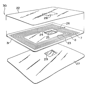
Figure 9 illustrates a second example of a chip card 30 according to the
invention.
In this example, the card is constituted by a printed circuit 31, for
example a double-face printed circuit according to the example of Figure 4,
CA 02260885 2007-04-16
WO 98104105 PCTlcN96100262
-13-
mounted between a lower protective sheet 27 and an upper protective sheet
22. The sheets 22 and 27 are mounted on the printed circuit 31 by any known
means, for example by gluing, then possibly printed. In this variant, the
printed
circuit 31 will preferably have a minimal thickness, even though comprising.
if
necessary, a plurality of conducting layers on each face. Accommodations 28,
respectiveiy 29, are thus provided in the lower sheet 27 and in the upper
sheet
22 for the integrated circuit 25. Of course, depending upon the application,
it Is
likewise possible to use a single accommodation 28 or 29 and/or rep{aoe at
least one of the accommodations 28 or 29 with a window permitting acCees to
the circuit 25 or to the contacts connected to the circuit 25 from the
exterior of
, = the card.
It is evident that the variant of Figure 9 also applies to single-face
printed circuits 21.
Other methods of mounting of chip cards can be used with the printed
circuits according to the invention, for example the methods which are the
subject matter of the patent application W094l22111,
or one of the prior art methods mentioned In
that application.
Figure 10 ahows a printed circuit in an intermediate stage of
manufacture, according to a variant of the method intended to facilitate the
connection between the circuit 25 and the external portion 26 of the inductlve
element 23. This variant is intended, for examplQ, for security tags for
protection of inerchandise, but can also be applied to chip cards or to other
devices. A printed circuit including a portion in the shape of an inductive
oiomcnt 23 is machined In the way described above on a flexible substrate 1,
for example on a support of cardboard. The Inductive element 23 occupies
only about half of the total surface of the substrate 1. One of the ends 26 af
the
Inductive element 23 extends on the other half of the sfieet 21. This end can,
CA 02260885 1999-01-14'
WO 98/04105 PCTICH96/00262
-14-
for example, be constituted by a discrete wire soldered to the external
portion
of the inductive element 23. In a variant, this end 26 is machined by incision
in
the superficial conducting layer 2, in the way described above. The rest of
the
superficial layer 2 on this half of the sheet 21 can then be detached by
leaving
only the end 26 remaining.
An electronic or electric element 25 is mounted in a zone of the sheet
21 not occupied by the conducting paths, in this example on the inside of the
inductive element 23. The component 25 can be, for example, an integrated
circuit or a fuse. It is connected to the internal portion of the inductive
element
23 by way of a zone of conductive contact 51. In addition, the element 25 is
connected to a second zone of conductive contact 52 intended to establish the
connection with the end 26 of the inductive element 23.
After machining of conducting paths constituting the coil and the
mounting of the element 25, the half of the sheet 21 occupied by the
conducting paths is covered with an insulating layer (not shown). To do this,
the inductive element 23 can, for example, be covered with a layer of
insulating lacquer or an insulating adhesive sheet. The zone of contact 52,
however, is not covered by the insulating layer.
The sheet 21 is then folded over on itself along a folding axis 53 so that
the two halves mentioned are superimposed. The end 26 of the inductive
element 23 is thus put into electrical contact with the zone of contact 52. A
connection is thus formed very simply between the external portion of the
inductive element 23 and the element 25. The two folded halves of the sheet
21 can be fixed with respect to one another, for example by gluing.
The method according to the invention is also perfectly suitable for
production of flexible printed circuits. Such circuits are used, for example,
to
manufacture flexible plug connectors. Moreover the method is perfectly
CA 02260885 1999-01-14
WO 98/04105 PCTICH96/00262
-15-
adapted to any case where a maximal density of paths on the surface of a
printed circuit must be obtained.
One skilled in the art will realise moreover that the method can also be
used in combination with any other known method of printed circuit
manufacture. It is possible, for example, to make cards on which part of the
conducting paths are obtained or separated by electrochemical means, the
rest being machined in the way specified in the claims.
One skilled in the art will realise that the term "printed circuit" has been
used in this specification and in the claims by convention even though the
invention applies particularly to circuits and to cards produced without the
step
of printing in the usual sense.